
Effect of guanidinium on mesoscopic perovskite solar cells†
Xiaomeng
Hou
,
Yue
Hu
,
Huawei
Liu
,
Anyi
Mei
,
Xiong
Li
,
Miao
Duan
,
Guoan
Zhang
,
Yaoguang
Rong
* and
Hongwei
Han
*
School of Chemistry and Chemical Engineering, Wuhan National Laboratory for Optoelectronics, Huazhong University of Science and Technology, Wuhan 430074, Hubei, P. R. China. E-mail: ygrong@mail.hust.edu.cn; hongwei.han@mail.hust.edu.cn
First published on 16th November 2016
Abstract
Hole-conductor-free printable mesoscopic perovskite solar cells based on a TiO2/ZrO2/carbon architecture have attracted much attention due to their low material cost and simple fabrication process. However, the micron-thick mesoporous scaffold always challenges the filling of the perovskite absorber and causes significant charge carrier loss. We employ a multifunctional additive of guanidinium chloride (GuCl) to improve the quality of the CH3NH3PbI3 perovskite absorber, and suppress the recombination reaction in the device. It is found that GuCl effectively enhances the charge carrier lifetimes of the perovskite, and suppresses charge carrier loss in the hole-conductor-free devices. Correspondingly, the open-circuit voltage (VOC) of the device is significantly enhanced from 0.88 V to 1.02 V.
Introduction
Over the past few years, organic–inorganic hybrid perovskites have attracted significant attention as light absorbers in efficient photovoltaics. This mainly stems from their appealing features such as strong light absorption, excellent ambipolar charge mobility, small exciton binding energy, tunable band gaps, tolerance to defects and low-cost fabrication processes.1–6 Since the first reported perovskite absorber used for photovoltaic applications,1 the power conversion efficiency (PCE) of perovskite solar cells (PSCs) has rocketed to certified 22.1% (ref. 7) in just five years, which makes PSCs a serious contender to rival the leading photovoltaic technologies. However, most efficient PSCs usually require expensive hole-transport-materials (HTMs) such as 2,2′,7,7′-tetrakis(N,N-di-p-methoxy-phenylamine)-9,9′-spirobifluorene (spiro-OMeTAD) and noble metals such as Au and Ag.8,9 Not only the high material cost but also the energy intensive process (high vacuum conditions) will limit the large-scale commercial production of conventional structure PSCs.10To reduce the cost and simplify the device fabrication process, a hole-conductor-free fully printable mesoscopic PSC (MPSC) using the structure of FTO/TiO2/ZrO2/carbon/perovskite has been developed.11 Besides their cost effective device design, such printable MPSCs have showed incomparable stability under ambient conditions and sunlight. Recently, various efforts such as employing mixed-cation and mixed-anion perovskites,12,13 tuning the crystallization of perovskites,14 and introducing interface modifications15 have been carried out to improve the device performance. However, the micron-thick mesoscopic layers have been challenging the charge transportation, and thus the devices suffered from drastic charge recombination under working conditions. Accordingly, the relatively low open-circuit voltage (VOC) hindered the further improvement of the device performance.
In order to effectively mitigate the charge carrier loss, it is necessary to suppress recombination pathways within the perovskite and device. Employing additives in typical perovskite methylammonium lead iodide (MAPbI3) seems to be a facile method to tune its properties such as defect density and charge carrier lifetime, and suppress the recombination. Recently, Abate and co-workers used an iodopentafluorobenzene post-treatment to passivate under-coordinated iodide ions in MAPbI3.16 Similarly, H. Snaith's group used Lewis bases, thiophene and pyridine, to passivate under-coordinated Pb ions and achieve the carrier lifetimes of perovskite films up to 2 μs.17 Y. Yang's group demonstrated that guanidinium ions can suppress the recombinations.18
Herein, we employ an additive of guanidinium chloride (GuCl) in MAPbI3 and deposit the perovskite absorber with a simple one-step method to fabricate hole-conductor-free printable MPSCs. It is found that GuCl effectively improves the quality of the perovskite absorber in the mesoscopic triple-layer, and meanwhile suppresses the charge recombination reaction in the device, leading to a VOC of over 1.0 V. This facile method for improving the voltage of PSCs provides a promising strategy towards efficient photovoltaics.
Results & discussion
Fig. 1a depicts the device configuration of a typical printable MPSC with the triple-layer TiO2/ZrO2/carbon architecture.11,12 The mesoporous TiO2 (m-TiO2), perovskite, ZrO2 and carbon layer act as an electron collecting layer, light harvesting layer, insulating layer and hole collecting layer, respectively. A compact-TiO2 (c-TiO2) layer is sprayed between the FTO glass substrate and m-TiO2 to prevent the direct contact of the FTO and perovskite. All the mesoporous layers are deposited by screen printing.19 The perovskite absorber is filled in the triple-layer scaffold by a simple one-step method. The energy levels of the layers in the device are displayed in Fig. 1b. The perovskite MAPbI3 with a band gap of 1.50 eV is hosted by the triple-layer scaffold. Efficient electron extraction from the MAPbI3 conduction band (−3.93 eV) to the TiO2 (−4.0 eV) layer and hole collection from the MAPbI3 valence band (−5.43 eV) to the carbon (−5.0 eV) layer have been established. Significantly, the quality of the perovskite absorber determines the light harvesting efficiency and charge transportation, and the contact at the interfaces of TiO2/perovskite and perovskite/carbon determines the charge transfer in the device without a HTM layer.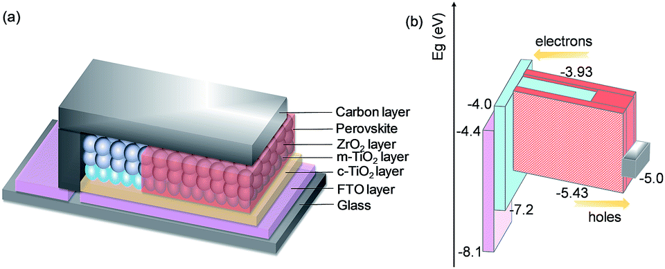 | ||
| Fig. 1 (a) Schematic of a printable mesoscopic perovskite solar cell with the architecture of FTO/c-TiO2/m-TiO2/ZrO2/carbon/perovskite; (b) energy level diagram of the device. | ||
UV-vis absorption spectral measurements were carried out to investigate the effect of GuCl on the optical properties of MAPbI3 (Fig. 2a). The samples were prepared by spin coating the precursor on m-TiO2 coated FTO substrates. When GuCl was added in MAPbI3 at a ratio of 0.25, the absorption of the perovskite film significantly enhanced in the range of 400–600 nm without the shift of the onset. When the ratio of GuCl increased to 0.50 and then to 1.0, the absorption of the perovskite film reduced continuously. Since the absorption tails stayed almost unchanged for all the samples, we considered that the band gap of MAPbI3 remained relatively unaffected with Gu incorporation.
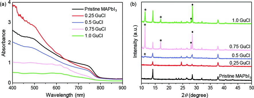 | ||
| Fig. 2 UV-vis absorption spectra (a) and XRD spectra (b) of pristine MAPbI3 and MAPbI3·xGuCl (x = 0, 0.25, 0.5, 0.75 and 1.0). | ||
To evaluate the structural impacts of Gu on the perovskite crystals, X-ray diffraction (XRD) analysis was conducted, as presented in Fig. 2b. For MAPbI3·xGuCl with x = 0.05–0.4, the crystal structure was found to be identical to that of the pristine MAPbI3 tetragonal perovskite phase, as indicated by the peaks at 14.04°, 28.47°, 31.92°, 40.39° and 43.10° for the (110), (220), (310), (224) and (314) crystal planes (see Fig. S1†).20 This demonstrated that the growth of the perovskite crystals was not structurally affected by the addition of GuCl. In contrast, when the ratio of GuCl was increased to over 0.5, a significant evolution of XRD patterns was observed. For MAPbI3·0.5GuCl, a new peak at 11.32° appeared, which might belong to the hexagonal GuPbI3.21 For MAPbI3·0.75GuCl and MAPbI3·1.0GuCl, a peak at 17.00° that corresponds to the hexagonal GuPbI3 was observed. At the same time, the peak at 28.47° separated into two peaks at 28.02° and 28.52°, which belonged to the orthorhombic GuPbI3. Therefore, we speculate that Gu has not been incorporated into the lattice of MAPbI3 at a relatively low ratio (x < 0.4). At a relatively high ratio (x > 0.5), the partial substitution of MA by Gu and formation of GuPbI3 will negatively affect the photovoltaic performance of the devices due to much reduced absorption, which is in accordance with the results of Y. Yang's group.
To correlate the addition of GuCl with the device performance, MAPbI3·xGuCl was infiltrated in the TiO2/ZrO2/carbon triple-layer to fabricate hole-conductor-free printable MPSCs, and the results are summarized in Table S1.† Compared with the pristine MAPbI3 based device, MAPbI3·0.25GuCl and MAPbI3·0.5GuCl based devices presented a much higher VOC (1.01 V and 1.02 V) and fill factor (FF, 0.74 and 0.72). We proposed that the enhanced VOC was attributed to the significantly suppressed recombination reaction in the device (vide infra). The variation in JSC was in agreement with the absorption results. Particularly, the device based on MAPbI3·0.25GuCl showed the highest short-circuit current density (JSC) of 17.06 mA cm−2. The enhanced absorption and JSC were considered to result from the improved morphology of the MAPbI3·xGuCl film. When x was further increased to 0.75 and 1.0, all the photovoltaic parameters of the devices rapidly decreased, especially the JSC, confirming the incorporation of Gu into the MAPbI3 lattice and formation of GuPbI3 will negatively affect the device performance due to reduced absorption. For the device based on pure GuPbI3 (Fig. S2†), the color of the absorber was pale yellow, and the device showed an efficiency of lower than 1% with a VOC of 0.82 V, a JSC of 2.74 mA cm−2 and a FF of 0.51.
There have been many reports on additives for tuning the crystal growth and properties of perovskite MAPbI3.18,22–24 However, most of them either improve the surface smoothness or passivate the grain boundaries of perovskite films through slowing down the crystallization. Here, the Gu cation is able to work as a cross-link between neighbouring grains in the perovskite film due to the ammonium groups.25–27 The interaction between Gu and MAPbI3 was confirmed by 1H NMR measurements. The 1H NMR results of GuCl, MAPbI3 and MAPbI3·xGuCl solution in deuterated N,N-dimethylformamide-d7 (DMF-d7) are shown in Fig. S3.† Resonance signals for the –C(NH2)3+⋯Cl− protons appear at δ = 7.67 ppm in the presence of GuCl and at δ = 7.37 ppm in the presence of GuCl accompanied by MAPbI3. Compared to the chloride ions, the iodide anions with lower electronegativity inductively withdrew less electron density out of the protons, which induced an upfield shift in the resonance signals. As a result, the N–H hydrogen signal undergoes an upfield shift of Δδ = 0.3 ppm, suggesting that the hydrogen-bonding interaction between –C(NH2)3+ and halide ions has changed from N–H⋯Cl− to N–H⋯I−. These three –NH2 groups may increase the linking of the neighbouring MAPbI3, thus helping the crystals grow in contact with each other more tightly, as shown in Fig. 3a.
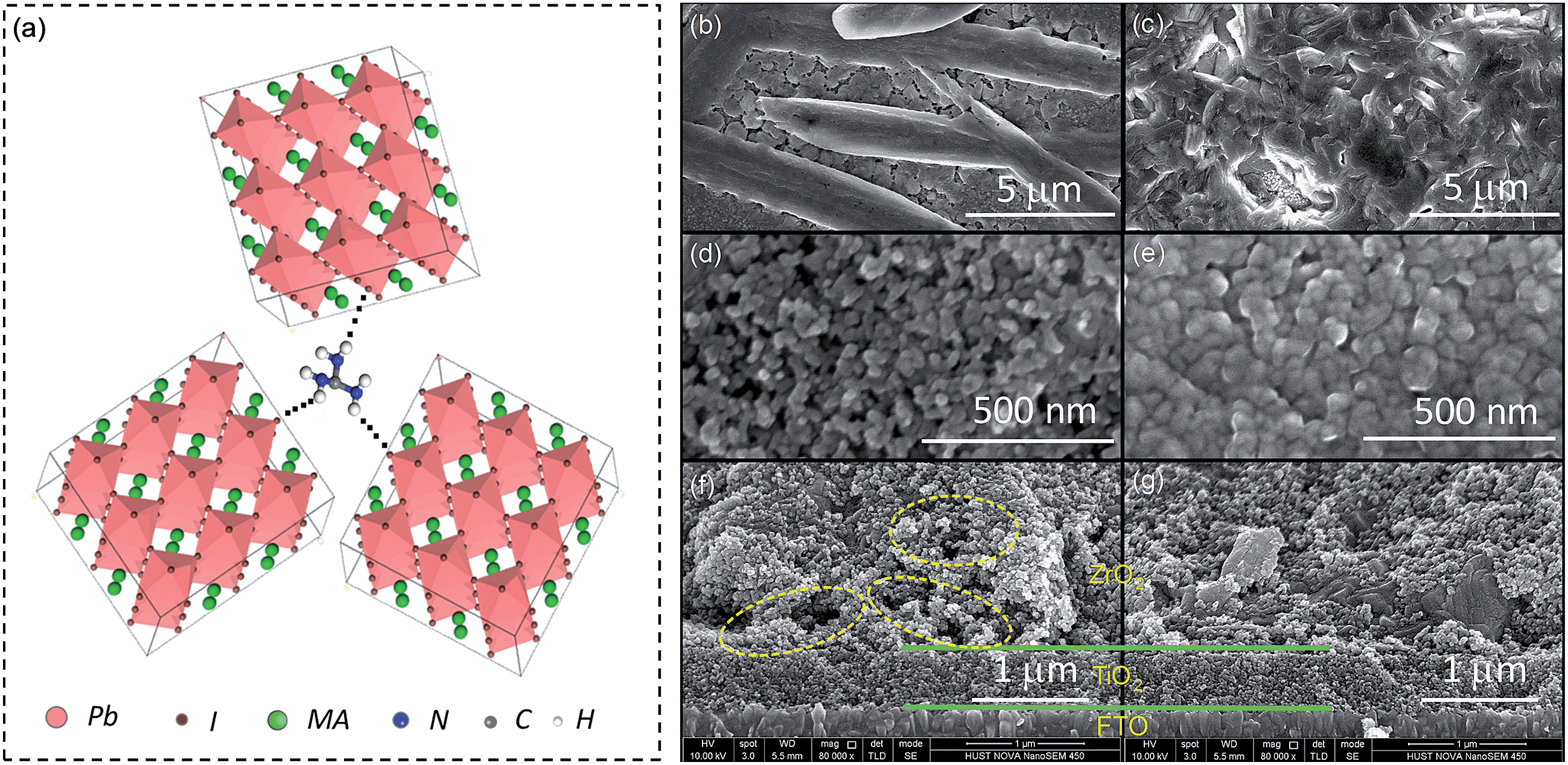 | ||
| Fig. 3 (a) Schematic illustration of three neighbouring grain structures crosslinked by hydrogen-bonding interactions (N–H⋯I) of the iodide with the ammonium end groups of GuCl species. (b and c) Top-view SEM images of MAPbI3 and MAPbI3·xGuCl films on FTO substrates. (d and e) Top-view SEM images of MAPbI3 and MAPbI3·xGuCl (x = 0.25) infiltrated mesoporous TiO2 films; (f and g) cross sectional SEM images of the mesoporous scaffold (TiO2/ZrO2) infiltrated with MAPbI3 and MAPbI3·xGuCl (x = 0.25). | ||
For pristine MAPbI3, the one-step deposition method usually results in a film with a rod/textile-like morphology.28 The non-compact distribution of perovskite crystals with a low coverage will lead to poor charge transportation and a weak light harvesting ability (Fig. 3b).29 Here, a smoother and more continuous film was obtained with the addition of GuCl (Fig. 3c). The effect of chlorine on the morphological evolution of the perovskite film has been well investigated previously.24,30,31 The improved morphology of the MAPbI3·xGuCl film could be attributed to the synergy of Gu and chlorine. Due to the improved morphology of MAPbI3·xGuCl films, better pore filling for the perovskite absorber in the mesoporous scaffold is expected. A thin perovskite layer was spun on a mesoporous TiO2 layer. It was found that MAPbI3·xGuCl achieved a complete filling in the nanopores of the TiO2 layer, and formed a continuous morphology (Fig. 3d and e). Furthermore, MAPbI3 and MAPbI3·xGuCl were infiltrated in the scaffold of TiO2/ZrO2/carbon. Large holes and void spaces in the MAPbI3 infiltrated scaffold were observed. In contrast, MAPbI3·xGuCl entirely penetrated into the scaffold and formed interconnected crystals. Such a compact morphology and complete filling will facilitate charge transportation in the micron-thick space layer and charge transfer at the interfaces of TiO2/perovskite and perovskite/carbon.
Photoluminescence spectroscopy was utilized to extract information regarding charge carrier dynamics,32–34 especially to evaluate the nonradioactive recombination loss in the MAPbI3 and MAPbI3·xGuCl. The perovskite films were prepared on ZrO2/glass substrates with an identical one-step deposition method as used for device fabrication, and steady-state PL and time-resolved PL (TRPL) measurements were carried out in ambient air. The enhanced PL intensity of MAPbI3·xGuCl (Fig. 4a) indicated that the nonradioactive recombination was significantly suppressed by the incorporation of GuCl. Interestingly, a blue shift of the peak position from 773 nm to 760 nm was also observed, which might be ascribed to the decreased trap state and reduced defect density of the MAPbI3·xGuCl film. For the charge carrier lifetimes, the MAPbI3·xGuCl film showed an enhanced τGu = 60.23 ns compared with τMA = 17.02 ns of the MAPbI3 film. The enhanced carrier lifetime should be attributed to inhibited electron–hole recombination in the perovskite film,35 and thus benefits charge transportation in the triple-layer scaffold.
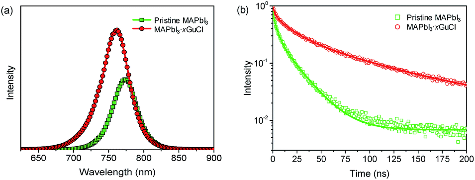 | ||
| Fig. 4 Comparison of the (a) steady-state PL intensities and (b) TRPL spectra of MAPbI3 and MAPbI3·xGuCl (x = 0.25) films deposited on ZrO2/glass substrates (the wavelength for monitoring the TRPL is 478 nm). | ||
Attributing to the improved morphology/pore filling and much longer charge carrier lifetime for MAPbI3·xGuCl, enhanced VOC and PCE have been obtained for our hole-conductor-free printable MPSCs. The representative J–V curves of MAPbI3 and MAPbI3·xGuCl based devices are presented in Fig. 5a. Compared with the device based on pristine MAPbI3 showing a VOC of 0.88 V, a JSC of 15.10 mA cm−2, a FF of 0.68 and a PCE of 9.10%, the device fabricated with MAPbI3·xGuCl presented a much higher VOC of 1.00 V, and a slightly enhanced JSC of 19.31 mA cm−2 and a FF of 0.743. The PCE was significantly enhanced to 14.35%. The incident photon-to-electron conversion efficiency (IPCE) spectra, which showed identical absorption tails for MAPbI3 and MAPbI3·xGuCl (Fig. 5b), confirmed that the band gap of the perovskite MAPbI3 has not been affected by the addition of GuCl. Fig. 5c–f compare the histograms of the photovoltaic parameters for devices based on MAPbI3 and MAPbI3·xGuCl. Since the JSC and FF of the MAPbI3·xGuCl based devices only slightly increased, the improvement in their PCE was mainly caused by the enhanced VOC, for which the average values are 0.88 V (MAPbI3) and 1.01 V (MAPbI3·xGuCl). It should be noted that the enhanced VOC of MAPbI3·xGuCl was quite reproducible, but the variations in the JSC and FF of the devices fabricated in one batch implied that the crystal growth of the perovskite still required further optimization.
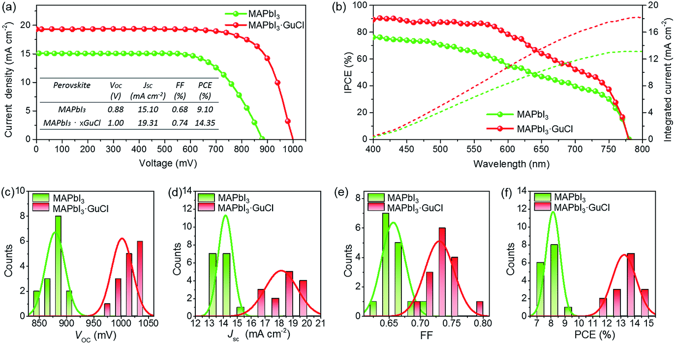 | ||
| Fig. 5 (a) J–V curves of hole-conductor-free printable MPSCs based on MAPbI3 and MAPbI3·xGuCl, and the corresponding photovoltaic parameters are plotted in the inset. (b) IPCE spectra and integrated current of MAPbI3 and MAPbI3·xGuCl based devices. (c–f) Comparison of the histograms of VOC, JSC, FF and PCE for devices based on MAPbI3 and MAPbI3·xGuCl (x = 0.25) (a batch of 15 devices). | ||
Despite the enhancement in the device performance, another critical issue remains in the current–voltage hysteresis of perovskite based photovoltaics.36 It has been reported that replacing MA with larger cation molecules could be essential for suppressing hysteresis.37 Here for the Gu contained perovskite with zero dipole moment, it was expected that hysteresis-free or hysteresis-less phenomena should be observed. However, the hysteresis effect was prominent for the MAPbI3·xGuCl based device (Fig. S4†). As reported previously,18 since Gu ions are on the perovskite grain surface without occupying the lattice of the perovskite, the ionic molecule would thus be responsive to an external electrical influence. Gu ions at interfaces or grain boundaries would migrate to the junction under the applied bias, thus aggravating the hysteresis effect.38 Nevertheless, a stabilized output at the maximum power point was measured under a bias of 0.82 V to confirm the accurate efficiency of the device, showing a PCE of 14.27% (Fig. S5†).
Impedance spectra (IS) are a useful tool to investigate the interfacial charge transport and recombination behaviours in photovoltaic devices.39–43 Herein it was recorded under dark conditions at a controlled bias (0 V to −1.0 V) in the frequency range from 100 mHz to 4 MHz to detect the interfacial performance of the hole-conductor-free MPSCs. Nyquist plots of MAPbI3·xGuCl and MAPbI3 at a bias of −0.8 V are shown in Fig. 6a together with the fitting results and equivalent circuit. Each Nyquist plot is composed of two semicircles, the starting point in the real part corresponds to the series resistance (Rs). The first small arc is attributed to the charge transfer resistance (Rct), which is responsible for hole transport in carbon and charge transfer/exchange at the interface of carbon/perovskite. And the second large arc is the recombination resistance (Rrec), reflecting the recombination reaction between the m-TiO2 and perovskite. No obvious difference in Rs was observed for MAPbI3 and MAPbI3·xGuCl based devices (Fig. 6b). However, for Rct and Rrec, it was found that the devices fabricated with MAPbI3·xGuCl exhibited a relatively smaller Rct at a given bias, indicating a more efficient charge transfer process at the carbon/perovskite interface (Fig. 6c). This should be attributed to the improved morphology of the MAPbI3·xGuCl layer in the mesoporous scaffold, which obtained a complete contact between the perovskite and carbon layer. At the same time, the MAPbI3·xGuCl based device also presented a rather higher charge recombination resistance, which is reasonable for the enhanced VOC (Fig. 6d). The Gu ions can be tightly absorbed on the TiO2 surface by electrostatic attraction to form a passivation layer, shielding the surface electrons against recombinations.44
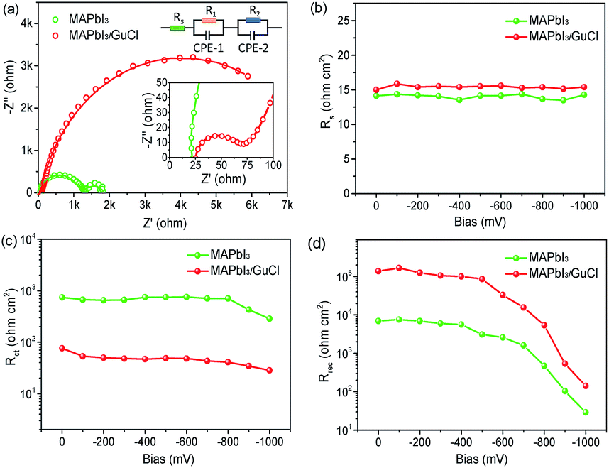 | ||
| Fig. 6 Impedance spectra of the devices. (a) Nyquist plots of devices based on MAPbI3 and MAPbI3·xGuCl at a bias of −0.8 V in the dark. Inset: the equivalent circuit. (b) Series resistance (Rs), (c) charge transfer resistance (Rct) and (d) recombination resistance (Rrec) at different biases extracted from impedance analysis of devices based on MAPbI3 and MAPbI3·xGuCl (x = 0.25). | ||
Conclusions
In summary, we investigated the effect of GuCl on MAPbI3 and a hole-conductor-free printable MPSC. GuCl effectively improved the morphology of the MAPbI3 through a one-step deposition method. With the assistance of both Cl− and N–H⋯I− hydrogen bonding between the Gu and the iodide anions on the perovskite surface, a decreased trap state and a reduced defect density for the perovskite film were obtained, accompanied by a longer carrier lifetime. The passivation of the TiO2 surface led to significantly suppressed recombination at the interface of TiO2/perovskite. Correspondingly, the voltage of the triple-layer based hole-conductor-free printable MPSCs was dramatically enhanced to over 1.0 V. The present study proposes further performance improvement of perovskite-based photovoltaics.Acknowledgements
The authors acknowledge financial support from the National Natural Science Foundation of China (51502141, 91433203, and 61474049), the Ministry of Science and Technology of China (863, 2015AA034601), and the Science and Technology Department of Hubei Province (2013BAA090).Notes and references
- A. Kojima, K. Teshima, Y. Shirai and T. Miyasaka, J. Am. Chem. Soc., 2009, 131, 6050–6051 CrossRef CAS PubMed.
- H.-S. Kim, C.-R. Lee, J.-H. Im, K.-B. Lee, T. Moehl, A. Marchioro, S.-J. Moon, R. Humphry-Baker, J.-H. Yum, J. E. Moser, M. Grätzel and N.-G. Park, Sci. Rep., 2012, 2, 591 Search PubMed.
- G. Xing, N. Mathews, S. Sun, S. S. Lim, Y. M. Lam, M. Grätzel, S. Mhaisalkar and T. C. Sum, Science, 2013, 342, 344–347 CrossRef CAS PubMed.
- G. E. Eperon, S. D. Stranks, C. Menelaou, M. B. Johnston, L. M. Herz and H. J. Snaith, Energy Environ. Sci., 2014, 7, 982–988 CAS.
- Q. Dong, Y. Fang, Y. Shao, P. Mulligan, J. Qiu, L. Cao and J. Huang, Science, 2015, 347, 967–970 CrossRef CAS PubMed.
- Y. Rong, Z. Ku, A. Mei, T. Liu, M. Xu, S. Ko, X. Li and H. Han, J. Phys. Chem. Lett., 2014, 5, 2160–2164 CrossRef CAS PubMed.
- NREL: http://www.nrel.gov/ncpv/images/efficiency_chart.jpg.
- J. H. Heo, S. H. Im, J. H. Noh, T. N. Mandal, C.-S. Lim, J. A. Chang, Y. H. Lee, H.-j. Kim, A. Sarkar, K. Nazeeruddin Md, M. Grätzel and S. I. Seok, Nat. Photonics, 2013, 7, 486–491 CrossRef CAS.
- J. M. Ball, M. M. Lee, A. Hey and H. J. Snaith, Energy Environ. Sci., 2013, 6, 1739–1743 CAS.
- Y. Rong, L. Liu, A. Mei, X. Li and H. Han, Adv. Energy Mater., 2015, 5, 1501066 CrossRef.
- Z. Ku, Y. Rong, M. Xu, T. Liu and H. Han, Sci. Rep., 2013, 3, 3132 Search PubMed.
- A. Mei, X. Li, L. Liu, Z. Ku, T. Liu, Y. Rong, M. Xu, M. Hu, J. Chen, Y. Yang, M. Grätzel and H. Han, Science, 2014, 345, 295–298 CrossRef CAS PubMed.
- J. Chen, Y. Rong, A. Mei, Y. Xiong, T. Liu, Y. Sheng, P. Jiang, L. Hong, Y. Guan, X. Zhu, X. Hou, M. Duan, J. Zhao, X. Li and H. Han, Adv. Energy Mater., 2016, 6, 1502009 CrossRef.
- Y. Tidhar, E. Edri, H. Weissman, D. Zohar, G. Hodes, D. Cahen, B. Rybtchinski and S. Kirmayer, J. Am. Chem. Soc., 2014, 136, 13249–13256 CrossRef CAS PubMed.
- L. Liu, A. Mei, T. Liu, P. Jiang, Y. Sheng, L. Zhang and H. Han, J. Am. Chem. Soc., 2015, 137, 1790–1793 CrossRef CAS PubMed.
- A. Abate, M. Saliba, D. J. Hollman, S. D. Stranks, K. Wojciechowski, R. Avolio, G. Grancini, A. Petrozza and H. J. Snaith, Nano Lett., 2014, 14, 3247–3254 CrossRef CAS PubMed.
- N. K. Noel, A. Abate, S. D. Stranks, E. S. Parrott, V. M. Burlakov, A. Goriely and H. J. Snaith, ACS Nano, 2014, 8, 9815–9821 CrossRef CAS PubMed.
- N. D. Marco, H. Zhou, Q. Chen, P. Sun, Z. Liu, L. Meng, E.-P. Yao, Y. Liu, A. Schiffer and Y. Yang, Nano Lett., 2016, 16, 1009–1016 CrossRef CAS PubMed.
- Y. Rong and H. Han, J. Nanophotonics, 2013, 7, 073090 CrossRef.
- T. Baikie, Y. Fang, J. M. Kadro, M. Schreyer, F. Wei, S. G. Mhaisalkar, M. Grätzel and T. J. White, J. Mater. Chem. A, 2013, 1, 5628–5641 CAS.
- L. Dimesso, A. Quintilla, Y. M. Kim, U. Lemmer and W. Jaegermann, Mater. Sci. Eng., B, 2016, 204, 27–33 CrossRef CAS.
- D. Bi, P. Gao, R. Scopelliti, E. Oveisi, J. Luo, M. Grätzel, A. Hagfeldt and M. K. Nazeeruddin, Adv. Mater., 2016, 28, 2910–2915 CrossRef CAS PubMed.
- W. Zhang, S. Pathak, N. Sakai, T. Stergiopoulos, P. K. Nayak, N. K. Noel, A. A. Haghighirad, V. M. Burlakov, D. W. deQuilettes, A. Sadhanala, W. Li, L. Wang, D. S. Ginger, R. H. Friend and H. J. Snaith, Nat. Commun., 2015, 6, 10030 CrossRef CAS PubMed.
- C. Zuo and L. Ding, Nanoscale, 2014, 6, 9935–9938 RSC.
- X. Li, M. Ibrahim Dar, C. Yi, J. Luo, M. Tschumi, S. M. Zakeeruddin, M. K. Nazeeruddin, H. Han and M. Grätzel, Nat. Chem., 2015, 7, 703–711 CrossRef CAS PubMed.
- D. B. Mitzi, C. A. Feild, W. Harrison and A. M. Guloy, Conducting tin halides with a layered organic-based perovskite structure, Nature, 1994, 369, 467–469 CrossRef CAS.
- I. C. Smith, E. T. Hoke, D. Solis-Ibarra, M. D. McGehee and H. I. Karunadasa, Angew. Chem., Int. Ed., 2014, 53, 11232–11235 CrossRef CAS PubMed.
- Y. Rong, Z. Tang, Y. Zhao, X. Zhong, S. Venkatesan, H. Graham, M. Patton, Y. Jing, A. M. Guloy and Y. Yao, Nanoscale, 2015, 7, 10595–10599 RSC.
- Z. Tang, S. Tanaka, S. Ito, S. Ikeda, K. Taguchi and T. Minemoto, Nano Energy, 2016, 21, 51–61 CrossRef CAS.
- Y. Zhao and K. Zhu, J. Phys. Chem. C, 2014, 118, 9412–9418 CAS.
- Y. Chen, Y. Zhao and Z. Liang, Chem. Mater., 2015, 27, 1448–1451 CrossRef CAS.
- X. Wen, A. Ho-Baillie, S. Huang, R. Sheng, S. Chen, H. C. Ko and M. A. Green, Nano Lett., 2015, 15, 4644–4649 CrossRef CAS PubMed.
- Q. Chen, H. Zhou, Y. Fang, A. Z. Stieg, T.-B. Song, H.-H. Wang, X. Xu, Y. Liu, S. Lu, J. You, P. Sun, J. McKay, M. S. Goorsky and Y. Yang, Nat. Commun., 2015, 6, 7269 CrossRef CAS PubMed.
- J. You, Y. Yang, Z. Hong, T.-B. Song, L. Meng, Y. Liu, C. Jiang, H. Zhou, W.-H. Chang, G. Li and Y. Yang, Appl. Phys. Lett., 2014, 105, 183902 CrossRef.
- G.-J. A. H. Wetzelaer, M. Scheepers, A. M. Sempere, C. Momblona, J. Ávila and H. J. Bolink, Adv. Mater., 2015, 27, 1837–1841 CrossRef CAS PubMed.
- H.-S. Kim, I.-H. Jang, N. Ahn, M. Choi, A. Guerrero, J. Bisquert and N.-G. Park, J. Phys. Chem. Lett., 2015, 6, 4633–4639 CrossRef CAS PubMed.
- J. Haruyama, K. Sodeyama, L. Han and Y. Tateyama, J. Am. Chem. Soc., 2015, 137, 10048–10051 CrossRef CAS PubMed.
- C. Eames, J. M. Frost, P. R. F. Barnes, B. C. O/'Regan, A. Walsh and M. S. Islam, Nat. Commun., 2015, 6, 7497 CrossRef CAS PubMed.
- A. Dualeh, T. Moehl, N. Tétreault, J. Teuscher, P. Gao, M. K. Nazeeruddin and M. Grätzel, ACS Nano, 2014, 8, 362–373 CrossRef CAS PubMed.
- H.-S. Kim, J.-W. Lee, N. Yantara, P. P. Boix, S. A. Kulkarni, S. Mhaisalkar, M. Grätzel and N.-G. Park, Nano Lett., 2013, 13, 2412–2417 CrossRef CAS PubMed.
- F. Zhang, X. Yang, M. Cheng, J. Li, W. Wang, H. Wang and L. Sun, J. Mater. Chem. A, 2015, 3, 24272–24280 CAS.
- X. Xu, Z. Liu, Z. Zuo, M. Zhang, Z. Zhao, Y. Shen, H. Zhou, Q. Chen, Y. Yang and M. Wang, Nano Lett., 2015, 15, 2402–2408 CrossRef CAS PubMed.
- L. Lu, T. Xu, W. Chen, J. M. Lee, Z. Luo, I. H. Jung, H. I. Park, S. O. Kim and L. Yu, Nano Lett., 2013, 13, 2365–2369 CrossRef CAS PubMed.
- Z. Zhang, N. Evans, S. M. Zakeeruddin, R. Humphry-Baker and M. Grätzel, J. Phys. Chem. C, 2007, 111, 398–403 CAS.
Footnote |
| † Electronic supplementary information (ESI) available. See DOI: 10.1039/c6ta08418d |
| This journal is © The Royal Society of Chemistry 2017 |