
Plasma-enhanced atomic layer deposition of titanium phosphate as an electrode for lithium-ion batteries†
Thomas
Dobbelaere
 *a,
Felix
Mattelaer
a,
Amit Kumar
Roy
a,
Philippe
Vereecken
b and
Christophe
Detavernier
*a
*a,
Felix
Mattelaer
a,
Amit Kumar
Roy
a,
Philippe
Vereecken
b and
Christophe
Detavernier
*a
aDepartment of Solid State Sciences, Ghent University, Krijgslaan 281 S1, 9000 Gent, Belgium. E-mail: thomas.dobbelaere@ugent.be; christophe.detavernier@ugent.be
bIMEC, Kapeldreef 75, 3001 Leuven, Belgium
First published on 22nd November 2016
Abstract
Titanium phosphate thin films were deposited by a new plasma-enhanced atomic layer deposition process. The process consisted of sequential exposures to trimethyl phosphate (TMP, Me3PO4) plasma, O2 plasma and titanium isopropoxide (TTIP, Ti(OCH(CH3)2)4) vapor, and it was characterized by in situ spectroscopic ellipsometry and ex situ X-ray reflectometry. The growth linearity, growth per cycle (GPC), and density of the resulting thin films were investigated as a function of the pulse times and the substrate temperature. The conformality of the process was characterized by deposition on micropillars. At a substrate temperature of 300 °C and using saturated pulse times, linear growth with a GPC of 0.66 nm per cycle and without nucleation delay was achieved. The as-deposited films were amorphous, while crystalline TiP2O7 was formed upon annealing in air or helium atmospheres. In lithium-ion test cells, the as-deposited films showed insertion and extraction of Li+ around a potential of 2.7 V vs. Li/Li+. Charge/discharge measurements revealed a volumetric capacity of 330 mA h cm−3, together with a good rate capability and minimal capacity fading.
Introduction
Atomic layer deposition (ALD) is a thin film deposition technique wherein a material is deposited onto a surface by alternating exposures to chemical precursor vapors. In contrast to chemical vapor deposition (CVD), the precursors are introduced separately, with pumping or purging steps in between them. This causes self-limiting reactions to take place on the substrate surface, resulting in layer-by-layer film growth. The advantages of ALD over CVD include better step coverage (enabling the conformal coating of 3D structures), lower temperature deposition (enabling deposition on temperature-sensitive substrates), and insensitivity to process variations (in a saturated regime, the growth rate is inherently constant, even when the precursor exposure varies).1 Many ALD processes exist for oxides, II–VI and III–V semiconductors, metal nitrides, metals, metal sulfides, and fluorides.2 A limited number of ALD processes for phosphates have been reported.3–17 ALD of titanium phosphate has only been reported twice, and in both cases, the metal precursor was titanium tetrachloride.9,10 In order to avoid the risk of any chlorine contamination in deposited films and eliminate corrosive hydrogen chloride as a byproduct, it is favourable to have a chlorine-free ALD process for this material.One way to achieve this would be to react phosphoric acid with titanium isopropoxide (TTIP). This has been previously demonstrated in a “liquid ALD” process, based on alternate dipping of the substrate in solutions of TTIP and phosphoric acid, which resulted in layer-by-layer growth of titanium phosphate.18 However, to use the same reaction chemistry for vapor phase ALD, one would need to evaporate both precursors. This is easy enough for TTIP, which reaches a suitable vapor pressure upon moderate heating, but impossible for phosphoric acid, which only evolves water by dehydration when heated. An alternative phosphorus precursor is trimethyl phosphate (TMP), a stable and cheap liquid which easily develops sufficient vapor pressure. However, TMP will not directly react with most metal–organic precursors because of the terminal methyl group in its molecular structure.
This problem can be solved by incorporating TMP vapor in an inductively coupled plasma and using this as the phosphorus precursor. We first explored this idea in a plasma-enhanced atomic layer deposition (PE-ALD) process for aluminium phosphate, where we investigated the reaction mechanism by in situ methods to reveal the function of the TMP plasma.7 In short, we concluded that the combined action of TMP plasma with O2 plasma created phosphoric acid-like precursor species on the substrate surface, which could subsequently react with a metal precursor. We have since successfully used TMP plasma in new PE-ALD processes for iron phosphate and zinc phosphate, which yielded exceptionally high growth rates while still showing self-limited behavior.19,20 In this work, titanium isopropoxide (TTIP) was used as the metal precursor, and this resulted in the plasma-enhanced atomic layer deposition of titanium phosphate.
Titanium phosphate is useful because of its ion-exchange properties and because of its catalytic activity.21,22 It can also be used as an intercalation-type electrode material for lithium-ion batteries. Crystalline pyrophosphate TiP2O7 has a reported redox potential of 2.6 V vs. Li/Li+, which makes it suitable as a cathode in conventional lithium-ion batteries, or −0.4 V vs. standard hydrogen, which makes it highly interesting as an anode for aqueous lithium-ion batteries.23–25 We will show that our as-deposited (amorphous) titanium phosphate thin films are similarly active, accommodating the insertion and extraction of lithium ions at a potential of 2.7 V vs. Li/Li+.
Experimental
Deposition system
Depositions were carried out in a home-built pump-type PE-ALD reactor shown schematically in Fig. 1. All parts were made of stainless steel, unless otherwise specified. The deposition chamber was continuously evacuated by using a turbomolecular pump to a base pressure of approx. 4 × 10⁻⁶ mbar. Precursor vapors and gases were admitted through computer-controlled pneumatic valves. The TMP (Sigma-Aldrich, 97%) and TTIP (Sigma-Aldrich, 97%) precursor bottles were heated to resp. 45 °C and 60 °C, so that they both reached pressures of approx. 5 × 10⁻³ mbar in the deposition chamber. The flow of O2 was adjusted to reach a pressure of 5 × 10⁻³ mbar in the deposition chamber. The temperature of the chamber walls was set to 130 °C, and all precursor tubes leading to the chamber were additionally heated to prevent any precursor condensation. On top of the chamber, a gate valve led to a fused quartz column wrapped by a copper coil. The coil was connected to a 13.56 MHz RF generator (ENI GHW-12Z) and a matching network in order to generate an inductively coupled plasma in the column. The remote plasma was generated by feeding vapor or gas from the chamber to the plasma column through the gate valve and pulsing the RF generator. The plasma power was set to 200 W for the TMP plasma and 300 W for the O2 plasma, and the impedance matching was tuned to minimize the reflected power on both. The substrates were mounted to a heated copper block, the temperature of which was PID-controlled. Depositions were performed on pieces of standard p-type silicon (100) wafer (for process characterization), silicon micropillar arrays (for conformality evaluation), or silicon wafer coated with platinum (where the platinum coating functioned as a lithium ion diffusion barrier and as a current collector for electrochemical characterization).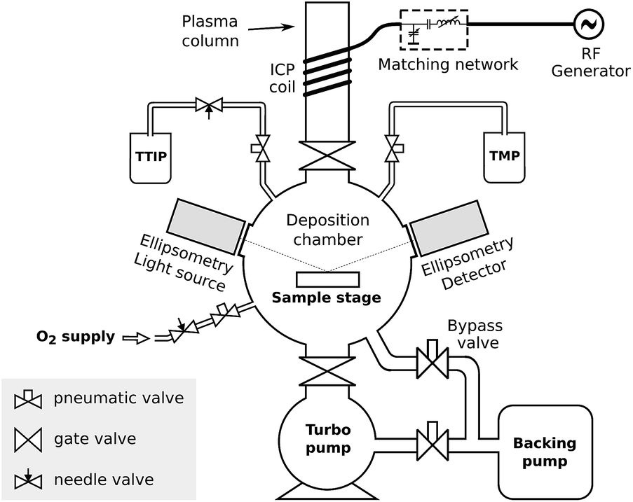 | ||
| Fig. 1 Schematic drawing of the deposition system used in this work, showing the vacuum chamber, the precursor connections, and the plasma system. | ||
Deposition process
A single cycle of a typical deposition process consisted of TMP plasma exposure–pumping–O2 plasma exposure–pumping–TTIP exposure–pumping. In between precursor pulses, pumping times of 20 s were found sufficient to bring residual pressures to below 4 × 10⁻⁵ mbar, thereby avoiding CVD side reactions.Material characterization
In situ spectroscopic ellipsometry measurements were performed with a J.A. Woollam M-2000 ellipsometer working in the ultraviolet-visible region and using the CompleteEASE software for fitting and data analysis. Measurements were acquired after each deposition cycle. Systematic parameters (angle offsets and window corrections) were fitted prior to deposition and then held fixed. The final thickness and the optical model parameters were fitted to the measurement acquired after the last cycle (i.e. after deposition). A growth curve was then obtained by fitting the thickness to each measurement, keeping all other parameters fixed. An FEI Quanta 200 F scanning electron microscope was used for SEM imaging, with the electron beam energy set to 10 keV and using an EDAX silicon-drift detector for energy-dispersive X-ray spectroscopy (EDX). X-ray reflectometry (XRR) patterns were acquired on Bruker D8 diffractometers using Cu Kα radiation. The film thickness and density were determined by XRR by fitting simulated patterns to the measured ones. In situ X-ray diffraction (XRD) during annealing was performed in a home-built setup.26–28 The annealing atmosphere was either helium or ambient air; the XRD patterns were acquired using a Cu Kα X-ray source and a position sensitive detector. X-ray Photoelectron Spectroscopy (XPS) analysis was performed on a Thermo Scientific Theta Probe XPS instrument using Al Kα X-rays generated at 15 kV and 70 W and focused to a spot with a size of 0.3 mm by using an MXR1 monochromator gun. To remove surface contamination, the sample surface was etched with Ar+ ions at an acceleration voltage of 3 keV and a current of 2 μA. Elastic recoil detection (ERD) measurements were carried out using an 8 MeV 35Cl4+ beam, with a scattering angle of 40° and a sample tilt of 20°.Electrochemical testing
Electrochemical test cells were constructed inside an argon-filled glovebox with O2 and H2O levels below 1 ppm. The working electrodes consisted of silicon substrates coated with PVD platinum (current collector) and then with PE-ALD titanium phosphate (active material). The cells consisted of a PTFE body filled with the electrolyte (1 M LiClO4 in propylene carbonate) clamped against the working electrode, with the coated side facing the liquid, and sealed by a circular O-ring defining an electrode area of 0.95 cm2. All reported currents and charges were normalized against this footprint area, yielding units of resp. μA cm−2 (current) and μA h cm−2 (charge). An electrical contact was made by applying conductive silver ink on the cleaved sides of the substrate in order to connect the platinum current collector layer to a piece of copper foil. The counter electrode and reference electrode consisted of lithium metal, thereby measuring all working electrode potentials against Li/Li+. Cyclic voltammetry and constant-current measurements were performed with home-built and commercial (Metrohm Autolab) potentiostat/galvanostat systems.Results and discussion
In situ growth monitoring
Film growth during the titanium phosphate depositions was monitored by in situ spectroscopic ellipsometry. In order to extract the film thickness from the optical data, one needs an optical model of the film, and the Tauc–Lorentz oscillator model was found to work best in this case. As shown in Fig. 2a, the measured psi and delta angles correspond well to the calculated ones for a range of film thicknesses between 1 and 33 nm, showing that the film thickness can be reliably extracted from the ellipsometry data. The model is also interesting in itself because it reveals the optical properties of the deposited film. The refractive index dispersion and absorption curves are plotted in Fig. 2b. The deposited material has a refractive index of 1.82 (defined at a wavelength of 589 nm), and an optical band gap of 2.96 eV. | ||
| Fig. 2 In situ spectroscopic ellipsometry during the titanium phosphate deposition process. (a) Psi and delta angles measured at three stages during film growth and compared with those calculated from the Tauc–Lorentz model using the film thickness as the only variable; (b) refractive index n and absorption coefficient k as a function of the wavelength. Both subfigures share the same wavelength axis. | ||
Fig. 3 shows the evolution of the film thickness at each cycle during a 50-cycle deposition process consisting of 50× [10 s TMP plasma–5 s O2 plasma–7 s TTIP vapor] at a substrate temperature of 300 °C. Linear growth is observed, without any nucleation delay, with a growth per cycle (i.e. the slope of the growth curve) of 0.66 nm per cycle. This is in perfect agreement with the ex situ XRR measurement shown in the inset of Fig. 3, where the interference fringes give a film thickness of 33 nm after 50 cycles. The prominent, non-decaying fringes in the XRR pattern also indicate that a smooth, low-roughness film was deposited.
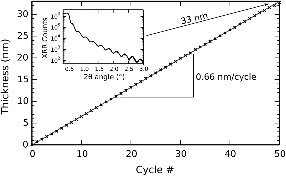 | ||
| Fig. 3 Film thickness as a function of the cycle number, fitted from in situ spectroscopic ellipsometry using the Tauc–Lorentz optical model. One cycle consisted of [10 s TMP plasma–5 s O2 plasma–7 s TTIP vapor] and the substrate temperature was 300 °C. Inset: XRR measurement of the resulting film (i.e. measured after 50 cycles). | ||
Saturation behavior
The effect of changing the (plasma) precursor exposures was investigated by varying the pulse times; with constant precursor pressures, the amounts of exposure are indeed proportional to the pulse times. This was done separately for each of the three precursor pulses by systematically performing depositions where one pulse time was varied while the other two were kept constant. The constant pulse times amounted to 10 s for TMP plasma, 5 s for O2 plasma, and 5 s for TTIP vapor. The substrate temperature was always kept constant at 300 °C. After each deposition, the film thickness and density were determined by XRR. Repeating this procedure for the TMP plasma, O2 plasma, and TTIP vapor pulses, one arrives at the plots in Fig. 4.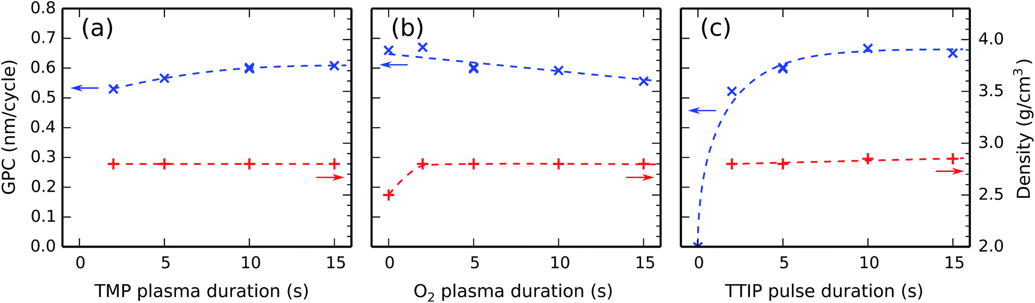 | ||
| Fig. 4 The GPC (left y-axes) and film density (right y-axes) as a function of (a) the TMP plasma, (b) the O2 plasma, and (c) the TTIP pulse durations at a substrate temperature of 300 °C. The three subfigures have identical y-scales. | ||
Fig. 4a indicates that the GPC increases slightly with the TMP plasma duration between 2 s and 10 s, and levels off after 10 s. The film density is independent of the TMP plasma duration and stays at a constant value of 2.8 g cm−3 in the investigated range.
Fig. 4b reveals a weak decrease of the GPC with the O2 plasma duration which continues over the whole investigated range. The film density is independent of the O2 plasma duration, unless there is no O2 plasma (the 0 s point), in which case the film density is significantly lower. As the O2 plasma's main function is to remove hydrocarbons from the surface species created by the TMP plasma, one may assume that the film density for the [TMP plasma–TTIP vapor] process is lower due to the inclusion of hydrocarbons in the deposited film.
Fig. 4c shows an initial sharp increase of the GPC with the TTIP pulse duration (there is no deposition in the absence of a TTIP pulse, at the 0 s point), which is followed by a flat region around 10 s. The film density is almost independent of the TTIP pulse duration.
In conclusion, all three exposures show saturating behavior, demonstrating the ALD nature of the process at 300 °C.
Temperature dependence
The effect of the substrate temperature on the deposition process was investigated by performing a series of depositions in the temperature range between 125 °C and 325 °C. The pulse times were kept at constant values of 10 s for TMP plasma, 5 s for O2 plasma, and 7 s for TTIP vapor, and were all sufficiently long to be in the saturated regions according to Fig. 4. The film thickness and density were determined by XRR, and the GPC was calculated by dividing the thickness by the number of cycles. The results are shown in Fig. 5b. For comparison purposes, the GPC of a process consisting of only TMP plasma pulses (15 s, followed by 15 s pumping) measured by in situ spectroscopic ellipsometry is plotted on the same temperature axis in Fig. 5a.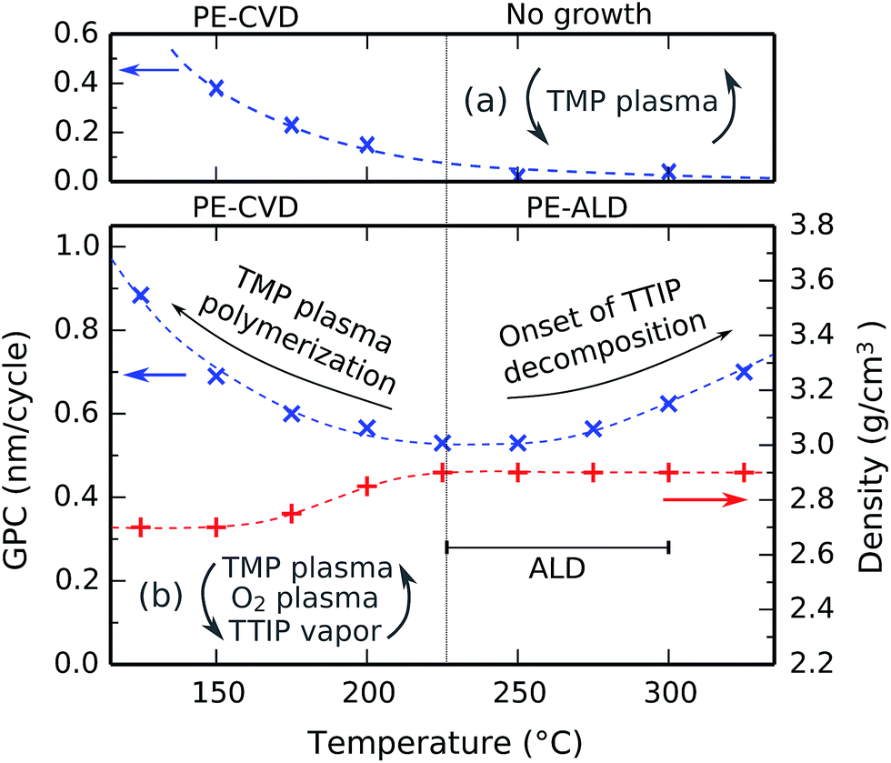 | ||
| Fig. 5 Growth per cycle as a function of the substrate temperature, as determined for repeated cycles of (a) only TMP plasma and (b) the full process (additionally showing the film density on the right y-axis). The PE-CVD and PE-ALD regions are indicated. | ||
Below 225 °C, lowering the temperature results in an increasing GPC and a decreasing film density. This is caused by the plasma polymerization of TMP, which continuously deposits phosphorus-rich materials in a CVD growth mode. This effect gets progressively stronger at lower substrate temperatures, as illustrated in Fig. 5a and investigated in detail in previous studies.7 The resulting films are phosphorus-rich, which renders them hygroscopic because the P–O–P bonds are easily hydrolyzed. Above 225 °C, the plasma polymerization is almost fully inhibited, as shown on the high-temperature side of Fig. 5a. Because there is no longer a CVD component, we are left with an ALD process. The deposited films are then no longer hygroscopic, and the film density reaches a constant 2.9 g cm−3.
Above 275 °C, the GPC starts to increase with temperature. A similar behavior has been observed for TiO2 deposition from TTIP and H2O29,30 or TTIP and O2 plasma,31 and it is typically attributed to the thermal decomposition of the TTIP precursor, as studies show that the decomposition rate of TTIP increases strongly around this temperature.32,33 However, given the saturation behavior of the TTIP pulse at 300 °C in Fig. 4c, the contribution from thermal decomposition must still be negligible compared to the ALD contribution in each cycle. We therefore conclude that the process has an ALD window between 225 °C and 300 °C, as indicated by the horizontal bar in Fig. 5b.
Film composition
Using saturated pulse times and at a substrate temperature of 300 °C, a titanium phosphate film was deposited on a silicon substrate using 120 cycles of the aforementioned process, resulting in a layer with a thickness of approx. 80 nm. Material characterization was then carried out on this sample. An XPS analysis of the as-deposited material is shown in Fig. 6. The survey spectra show titanium, phosphorus and oxygen peaks; carbon is only present on the film surface from environmental contamination, and disappears almost completely after etching away some of the top surface and exposing the fresh “bulk” film material. No silicon is visible, indicating that the deposited film completely covers the silicon substrate surface. The absence of any other peaks indicates that the film is pure. | ||
| Fig. 6 XPS analysis of the deposited titanium phosphate film. The survey spectra show the presence of titanium, phosphorus, and oxygen in the bulk of the film (red spectrum) in addition to some carbon which is only present on the film surface (blue spectrum). The detailed C 1s, Ti 2p, P 2p, and O 1s regions are shown above the survey scans using the same color legend; the quantification areas are filled in light red. | ||
Using an energy scale calibration where the C 1s peak is assigned to a binding energy of 284.5 eV, we find peaks of Ti 2p3/2 at 459.2 eV, Ti 2p1/2 at 465.0 eV, P 2p at 133.6 eV (deconvoluted as P 2p3/2 at 133.4 eV and P 2p1/2 at 134.3 eV), and O 1s at 531.1 eV. The Ti 2p binding energies correspond to a Ti4+ oxidation state, similar to TiO2. The phosphorus and oxygen binding energies are typical for a phosphate, but they are insensitive to the exact kind of phosphate, so they cannot be used to discriminate between e.g. orthophosphate and pyrophosphate.34
Using the detailed Ti 2p, P 2p, and O 2p spectra acquired after sputtering, a quantification was performed by integration of the peak areas, subtraction of a Tougaard background,35 and correction with empirical atomic sensitivity factors as reported by Ward and Wood.36 This yielded an empirical stoichiometry of TiP2.0O5.8. This quantification is, however, subject to various errors, including stoichiometry deviations caused by preferential sputtering, uncertainties in the background determination, and a poor knowledge of the electron analyzer transmission function; as such, we estimate the relative error to be ±10%.
To get a more reliable and absolute quantitative analysis of the stoichiometry, the same film was analyzed by elastic recoil detection (ERD). Fig. 7 shows the resulting depth profile, along with the quantification results in a table inset. Because the depth information stems from atomic energy loss, which is proportional to the areal density (i.e. the product of the depth and the number density of atoms), the depth profile is primarily given as a function of the areal density. As the number density is unknown and might vary, an exact conversion to a depth in nm is not possible. However, based on linear scaling with the known film thickness, an approximate depth scale in nm is shown on the secondary (upper) x-axis.
 | ||
| Fig. 7 ERD depth profile of an 80 nm titanium phosphate film on a silicon substrate. The lower x-axis expresses the depth as a total areal density, while the upper x-axis shows an approximate conversion to a “real” depth (in nm). Titanium, phosphorus, and oxygen are distributed uniformly throughout the layer, along with a small amount of hydrogen; the corresponding atomic percentages are shown in the table inset. No carbon was detected. | ||
The ERD quantification leads to an empirical stoichiometry of TiP1.7O5.6, with 4% hydrogen and zero carbon. This should be regarded as the “true” stoichiometry of the as-deposited material, since the errors on the atomic percentages are only ±2% (which is much more accurate than the XPS quantification). This stoichiometry is somewhere in between titanium pyrophosphate (TiP2O7) and titanium orthophosphate (TiP1.3O5.3), and as such, the deposited material could be regarded as a mixture of both.
Conformality evaluation
In order to evaluate the ability of the process to penetrate 3D-structured substrates and coat them conformally, a titanium phosphate film was deposited on a silicon micropillar substrate using 120 cycles of [30 s TMP plasma–15 s O2 plasma–21 s TTIP vapor] (pulse times were chosen three times as long as required for saturation on the planar substrates) at 300 °C. The micropillar substrate consisted of an array of vertical pillars (50 μm long and 2 μm wide, arranged in a square lattice with a lattice spacing of 7 μm) etched into silicon.A side-view SEM image and EDX analysis of this sample are shown in Fig. 8. The Ti, P, and O intensities shown in the SEM image in Fig. 8a were determined by the integration of their corresponding Kα peaks in EDX spectra acquired along horizontal scans at different depths (three of these spectra are visible in Fig. 8b). In this way, the individual elemental amounts can be tracked along the penetration depth; this allows us to evaluate not only the total amount of material (i.e. the thickness), but also its composition, which may also vary along the penetration depth. Indeed, while the amount of titanium stays essentially constant along the pillars, the amount of phosphorus decreases by about 20% going from the top to the middle of the pillars. Between the middle and the bottom, it stays rather constant, but near the bottom another 20% decrease is observed. The amount of oxygen remains largely constant along the pillars but decreases by approx. 15% near the bottom. The pronounced differences in the behavior between elements are probably related to the fact that oxygen and phosphorus are introduced through plasma exposures, while the titanium comes from a vapor-phase precursor; it is known that plasma exposures do not easily penetrate within trench structures as the radicals get quickly depleted by recombination on the structure walls.37 We conclude that, even though the whole structure is coated with titanium phosphate, the amount of deposited material is not entirely constant and there are variations in the stoichiometry along the penetration depth.
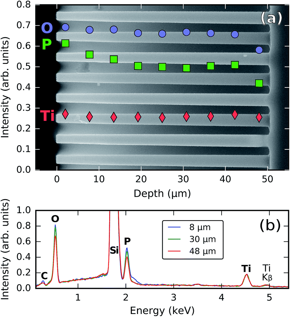 | ||
| Fig. 8 SEM/EDX analysis of a silicon micropillar array coated with titanium phosphate, showing (a) the intensities of the Ti, P, and O Kα signals as a function of the penetration depth inside the pillars and (b) the raw EDX spectra at three different depths. | ||
Film crystallinity
The crystallinity of the deposited titanium phosphate was studied by in situ XRD during annealing. A 90 nm thick film on a planar silicon substrate was heated from room temperature to 950 °C at a linear heating rate of 10 °C min−1 in a helium atmosphere, while XRD patterns were continuously acquired in a 2θ range of 19° to 36°. The result is shown in Fig. 9. The as-deposited film is amorphous, and stays amorphous until a temperature of 840 °C is reached. It then transforms into crystalline titanium pyrophosphate (TiP2O7, JCPDS #00-038-1468),38 and remains in this phase after cooling down back to room temperature.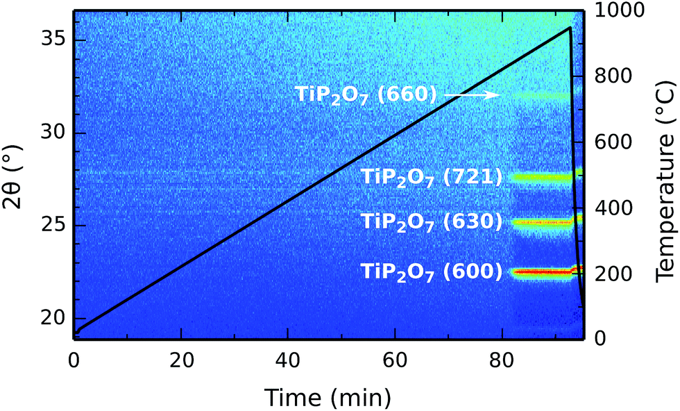 | ||
| Fig. 9 In situ XRD during annealing of a 90 nm thick titanium phosphate film in a helium atmosphere. The diffracted intensity is represented by color intensity as a function of the diffraction angle on the left y-axis and the elapsed time on the x-axis. The temperature profile is drawn by the black solid line, using the temperature scale on the right y-axis. | ||
The same measurement was also performed in air instead of helium (ESI Fig. S1†), with essentially the same result; the same crystallization behavior was observed, albeit with a higher crystallization temperature (890 °C).
Electrochemical lithiation
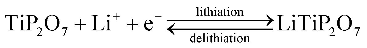
The Li+ insertion/extraction behavior of the as-deposited, amorphous titanium phosphate was first characterized by cyclic voltammetry. Right after the assembly of the test cell, an open-circuit potential of 3.5 V was measured. During the first scan in the cathodic direction (i.e. decreasing the potential) at 1 mV s−1, a lithiation peak was observed around 2.65 V with a total charge insertion of −1.20 μA h cm−2 (ESI Fig. S2; † charges were calculated by the integration of the measured current over the elapsed time, which is equivalent to determining the area under the CV peaks and dividing it by the scan rate). Subsequent scans at 1 mV s−1 revealed measured charges of +1.05 μA h cm−2 (oxidation) and −1.02 μA h cm−2 (reduction). The excess charge measured during the initial lithiation can be attributed to the formation of a solid-electrolyte interphase (SEI), which consumes lithium.39If we approximate the composition of the as-deposited material as TiP2O7 with a molar mass of 222 g mol−1, and use a thickness of 30 nm and a density of 2.8 g cm−3 (both measured by XRR), the measured charges correspond to the insertion and extraction of 1.0 moles of lithium per mole of TiP2O7. This means we have the following reaction:
In order to examine electrode kinetics, additional CV scans were acquired at scan rates of 1, 2, 5, 10, 20, and 50 mV s−1 between fixed potential limits of 2.3 V and 3.2 V. The resulting cyclic voltammograms (omitting the 20 mV s−1 and 50 mV s−1 scans to avoid the loss of detail on the 1 mV s−1 and 2 mV s−1 scans) are shown in Fig. 10, along with a plot of the anodic and cathodic peak currents (ip,a and ip,c) as a function of the scan rate ν (Fig. 10, inset). Given that the ratio ip,a/ip,c is significantly less than one, that the peak separation increases with the scan rate, and that the peak currents are not proportional to the square root of the scan rate (as predicted by the Randles–Sevcik equation for reversible processes), we can conclude that the Li+ insertion/extraction reactions at the electrode are electrochemically irreversible.40 Furthermore, both ip,a and ip,c are in good approximation proportional to ν0.8; this means that the redox reaction mechanism is neither a diffusion-limited one (where ip ∼ ν0.5) nor a surface-confined one (where ip ∼ ν), but is perhaps a combination of both.41
 | ||
| Fig. 10 Cyclic voltammetry measurements performed between 2.3 V and 3.2 V at scan rates ranging from 1 mV s−1 to 10 mV s−1 on a 30 nm as-deposited titanium phosphate film. The inset figure shows the absolute values of the anodic peak current ip,a and the cathodic peak current ip,c as a function of the scan rate ν between 1 and 50 mV s−1, together with fitted power laws (lines on the double-log scale). | ||
Charge/discharge cycling
Fig. 11a shows constant-current charge/discharge curves of the 30 nm titanium phosphate film. Using constant currents of ±1.02 μA cm−2 (negative sign for lithiation and positive sign for delithiation), corresponding to a 1C rate, between potential cut-offs of 2.3 V (lithiation) and 3.2 V (delithiation), lithiation and delithiation capacities of resp. 1.01 μA h cm−2 and 0.99 μA h cm−2 were measured. This yields a coulombic efficiency (defined as the delithiation capacity divided by the lithiation capacity) of 98.6%. Division of the surface-normalized capacity by the film thickness yields a volumetric capacity of 330 mA h cm−3; an additional division by the density of the material yields a gravimetric capacity of approx. 120 mA h g−1.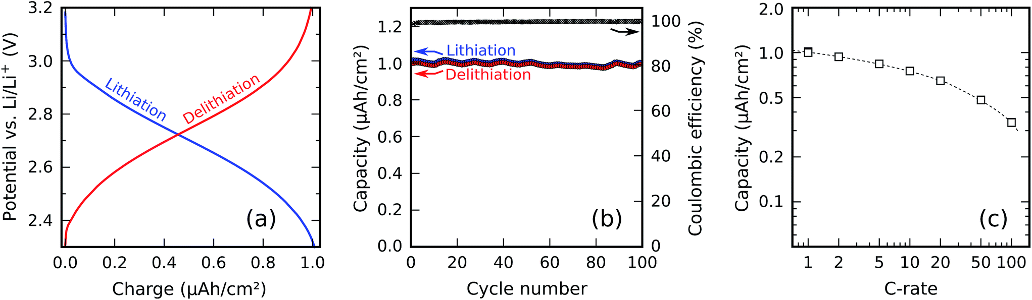 | ||
| Fig. 11 Constant-current charge/discharge testing of a 30 nm planar titanium phosphate electrode. (a) Voltage profiles during lithiation and delithiation at 1C; (b) capacity and coulombic efficiency measured over 100 charge/discharge cycles at 1C; (c) capacity as a function of the C-rate. | ||
Fig. 11b shows the behavior of the material upon repeated cycling, using the same 1C rate and the same potential limits as in the preceding measurement. The measured capacity as a function of the cycle number shows small temperature-related fluctuations together with a systematic decrease due to capacity fading; this decrease only amounts to a loss of 2.2% of the initial capacity after 100 cycles, indicating good cyclability and low capacity fading.
The rate capability of the electrode was investigated by measuring the available capacity for a range of charge/discharge currents between 1C and 100C. For each C-rate, three charge/discharge cycles were ran, and the capacity was determined in the third cycle; in this way, any effect from the preceding C-rates was erased. The same potential limits as previously mentioned were used, so at 1C, the measured capacity was identical to the one shown in Fig. 11b. The resulting plot of the capacity as a function of the C-rate is shown in Fig. 11c. At higher C-rates, the available capacity decreases; at a rate of 50C, approx. 50% of the 1C capacity remains.
Conclusions
Using pulses of TMP plasma, O2 plasma and TTIP vapor, a chlorine-free PE-ALD process for titanium phosphate was developed which worked in a temperature region between 225 °C and 300 °C. At a substrate temperature of 300 °C, precursor saturation and linear growth were observed, demonstrating ALD behavior with a GPC of 0.66 nm per cycle. Outside of this temperature region, the GPC increased; on the low-temperature side due to a CVD contribution from the TMP plasma, and on the high-temperature side due to the decomposition of the TTIP precursor. The films grown at 300 °C had a density of 2.8 g cm−3 and an empirical stoichiometry of TiP1.7O5.6 (measured by ERD); they were amorphous as-deposited, but could be crystallized to TiP2O7 by post-deposition annealing in air or helium atmospheres. A silicon micropillar test structure coated with this process showed variations in the amount and composition of the deposited material along the penetration depth, indicating imperfect conformality. The as-deposited material could be electrochemically lithiated and delithiated around 2.7 V vs. Li/Li+, showing a volumetric capacity of 330 mA h cm−3 (1.0 μA h cm−2 for a 30 nm film) and a coulombic efficiency of 98.9%. The material was stable, losing only 2.2% of its initial capacity after 100 cycles. The low film thickness resulted in a good rate capability, still retaining about 50% of the 1C capacity at a rate of 50C.Acknowledgements
The authors are grateful to the FWO Vlaanderen for providing Thomas Dobbelaere with financial support through the mandate of Aspirant. They also acknowledge the financial support from the UGENT-GOA-01G01513, Hercules AUGE/09/014, IWT-SBO SOSLion, and ERA-LaminaLion projects. They also thank Karl Opsomer for the XPS measurements and Olivier Janssens for SEM/EDX.References
- R. W. Johnson, A. Hultqvist and S. F. Bent, Mater. Today, 2014, 17, 236–246 CrossRef CAS.
- V. Miikkulainen, M. Leskelä, M. Ritala and R. L. Puurunen, J. Appl. Phys., 2013, 113, 021301 CrossRef.
- M. Nieminen, L. Niinistö and R. Lappalainen, Microchim. Acta, 1995, 119, 13–22 CrossRef CAS.
- M. Tiitta, E. Nykänen, P. Soininen, L. Niinistö, M. Leskelä and R. Lappalainen, Mater. Res. Bull., 1998, 33, 1315–1323 CrossRef CAS.
- J. Liu, Y. Tang, B. Xiao, T.-K. Sham, R. Li and X. Sun, RSC Adv., 2013, 3, 4492–4495 RSC.
- S. Knohl, A. K. Roy, R. Lungwitz, S. Spange, T. Mäder, D. J. Nestler, B. Wielage, S. Schulze, M. Hietschold, H. Wulff, C. A. Helm, F. Seidel, D. R. T. Zahn and W. A. Goedel, ACS Appl. Mater. Interfaces, 2013, 5, 6161–6167 CAS.
- T. Dobbelaere, A. K. Roy, P. Vereecken and C. Detavernier, Chem. Mater., 2014, 26, 6863–6871 CrossRef CAS.
- M. Putkonen, T. Sajavaara, P. Rahkila, L. Xu, S. Cheng, L. Niinistö and H. J. Whitlow, Thin Solid Films, 2009, 517, 5819–5824 CrossRef CAS.
- M. K. Wiedmann, D. H. K. Jackson, Y. J. Pagan-Torres, E. Cho, J. A. Dumesic and T. F. Kuech, J. Vac. Sci. Technol., A, 2012, 30, 01A134 Search PubMed.
- J. Hämäläinen, J. Holopainen, F. Munnik, M. Heikkilä, M. Ritala and M. Leskelä, J. Phys. Chem. C, 2012, 116, 5920–5925 Search PubMed.
- H. H. Sønsteby, E. Østreng, H. Fjellvåg and O. Nilsen, Chem. Vap. Deposition, 2014, 20, 269–273 CrossRef.
- J. Hämäläinen, J. Holopainen, F. Munnik, T. Hatanpää, M. Heikkilä, M. Ritala and M. Leskelä, J. Electrochem. Soc., 2012, 159, A259–A263 CrossRef.
- A. C. Kozen, A. J. Pearse, C.-F. Lin, M. Noked and G. W. Rubloff, Chem. Mater., 2015, 27, 5324–5331 CrossRef CAS.
- M. Nisula, Y. Shindo, H. Koga and M. Karppinen, Chem. Mater., 2015, 27, 6987–6993 CrossRef CAS.
- K. B. Gandrud, A. Pettersen, O. Nilsen and H. Fjellvåg, J. Mater. Chem. A, 2013, 1, 9054–9059 CAS.
- J. Liu, B. Xiao, M. N. Banis, R. Li, T.-K. Sham and X. Sun, Electrochim. Acta, 2015, 162, 275–281 CrossRef CAS.
- J. Liu, M. N. Banis, Q. Sun, A. Lushington, R. Li, T.-K. Sham and X. Sun, Adv. Mater., 2014, 26, 6472–6477 CrossRef CAS PubMed.
- G. Freiman, P. Barboux, J. Perrière and K. Giannakopoulos, Chem. Mater., 2007, 19, 5862–5867 CrossRef CAS.
- T. Dobbelaere, F. Mattelaer, J. Dendooven, P. Vereecken and C. Detavernier, Chem. Mater., 2016, 28, 3435–3445 CrossRef CAS.
- T. Dobbelaere, M. Minjauw, T. Ahmad, P. Vereecken and C. Detavernier, J. Non-Cryst. Solids, 2016, 444, 43–48 CrossRef CAS.
- G. Alberti, P. Cardini-Galli, U. Costantino and E. Torracca, J. Inorg. Nucl. Chem., 1967, 29, 571–578 CrossRef CAS.
- A. Clearfield and D. S. Thakur, Appl. Catal., 1986, 26, 1–26 CrossRef CAS.
- H. Wang, K. Huang, Y. Zeng, S. Yang and L. Chen, Electrochim. Acta, 2007, 52, 3280–3285 CrossRef CAS.
- Y. Uebou, S. Okada, M. Egashira and J.-I. Yamaki, Solid State Ionics, 2002, 148, 323–328 CrossRef CAS.
- W. Wu, S. Shanbhag, A. Wise, J. Chang, A. Rutt and J. F. Whitacre, J. Electrochem. Soc., 2015, 162, A1921–A1926 CrossRef CAS.
- W. Knaepen, C. Detavernier, R. L. Van Meirhaeghe, J. Jordan Sweet and C. Lavoie, Thin Solid Films, 2008, 516, 4946–4952 CrossRef CAS.
- W. Knaepen, S. Gaudet, C. Detavernier, R. L. V. Meirhaeghe, J. J. Sweet and C. Lavoie, J. Appl. Phys., 2009, 105, 083532 CrossRef.
- G. Rampelberg, M. Schaekers, K. Martens, Q. Xie, D. Deduytsche, B. De Schutter, N. Blasco, J. Kittl and C. Detavernier, Appl. Phys. Lett., 2011, 98, 162902 CrossRef.
- M. Ritala, M. Leskelä, L. Niinistö and P. Haussalo, Chem. Mater., 1993, 5, 1174–1181 CrossRef CAS.
- Q. Xie, J. Musschoot, D. Deduytsche, R. L. V. Meirhaeghe, C. Detavernier, S. Van Den Berghe, Y.-L. Jiang, G.-P. Ru, B.-Z. Li and X.-P. Qu, J. Electrochem. Soc., 2008, 155, H688–H692 CrossRef CAS.
- J. Lee, S. J. Lee, W. B. Han, H. Jeon, J. Park, W. Jang, C. S. Yoon and H. Jeon, Phys. Status Solidi A, 2013, 210, 276–284 CrossRef CAS.
- K. L. Siefering and G. L. Griffin, J. Electrochem. Soc., 1990, 137, 814–818 CrossRef CAS.
- Y.-M. Wu, D. C. Bradley and R. M. Nix, Appl. Surf. Sci., 1993, 64, 21–28 CrossRef CAS.
- C. Wagner, W. Riggs, L. Davis, J. Moulder and G. Muilenberg, Handbook of X-ray Photoelectron Spectroscopy: A Reference Book of Standard Data For Use In X-Ray Photoelectron Spectroscopy, Perkin-Elmer Corporation, 1979 Search PubMed.
- S. Tougaard, Surf. Sci., 1989, 216, 343–360 CrossRef CAS.
- R. J. Ward and B. J. Wood, Surf. Interface Anal., 1992, 18, 679–684 CrossRef CAS.
- C. Detavernier, J. Dendooven, D. Deduytsche and J. Musschoot, ECS Trans., 2008, 16, 239–246 CAS.
- H. F. McMurdie, M. C. Morris, E. H. Evans, B. Paretzkin, W. Wong-Ng, Y. Zhang and C. R. Hubbard, Powder Diffr., 1987, 2, 52 CrossRef.
- P. Verma, P. Maire and P. Novák, Electrochim. Acta, 2010, 55, 6332–6341 CrossRef CAS.
- N. Aristov and A. Habekost, World J. Chem. Educ., 2015, 3, 115–119 CAS.
- A. J. Bard and L. R. Faulkner, Electrochemical Methods: Fundamentals and Applications, John Wiley & Sons, Inc., New York, 2nd edn, 2000 Search PubMed.
Footnote |
| † Electronic supplementary information (ESI) available: XRD during air annealing and cyclic voltammogram showing the initial lithiation. See DOI: 10.1039/c6ta04179e |
| This journal is © The Royal Society of Chemistry 2017 |