
Enhancing the solar energy conversion efficiency of solution-deposited Bi2S3 thin films by annealing in sulfur vapor at elevated temperature†
Zhehao
Zhu‡
 ab,
Satish Kumar
Iyemperumal
b,
Kateryna
Kushnir
c,
Alexander D.
Carl
a,
Lite
Zhou
d,
Drew R.
Brodeur
a,
Ronald L.
Grimm
a,
Lyubov V.
Titova
c,
N. Aaron
Deskins
b and
Pratap M.
Rao
*de
ab,
Satish Kumar
Iyemperumal
b,
Kateryna
Kushnir
c,
Alexander D.
Carl
a,
Lite
Zhou
d,
Drew R.
Brodeur
a,
Ronald L.
Grimm
a,
Lyubov V.
Titova
c,
N. Aaron
Deskins
b and
Pratap M.
Rao
*de
aDepartment of Chemistry and Biochemistry, Worcester Polytechnic Institute, Worcester, MA 01609, USA
bDepartment of Chemical Engineering, Worcester Polytechnic Institute, Worcester, MA 01609, USA
cDepartment of Physics, Worcester Polytechnic Institute, Worcester, MA 01609, USA
dMaterials Science and Engineering Graduate Program, Worcester Polytechnic Institute, Worcester, MA 01609, USA. E-mail: pmrao@wpi.edu; Tel: +1 508-831-4828
eDepartment of Mechanical Engineering, Worcester Polytechnic Institute, Worcester, MA 01609, USA
First published on 26th September 2017
Abstract
Bi2S3 is a non-toxic n-type semiconductor, which has been commonly synthesized in the form of quantum dots or nanocrystalline films by solution deposition methods. Despite a favorable optical band gap of ∼1.3 eV, such films have not achieved high solar energy conversion efficiencies to date. We hypothesize that this is in part due to the presence of sulfur vacancies that, according to our density functional theory calculations, form a deep trap state in the band gap of Bi2S3, which can act as a strong recombination channel for photoexcited charges. Here, we report a microcrystalline Bi2S3 thin-film synthesized by annealing solution-deposited nanocrystalline Bi2S3 in a sulfur vapor environment at 445 °C, which simultaneously increases the grain size and phase purity of Bi2S3, fills in sulfur vacancies, and improves optical absorption. Time-resolved terahertz spectroscopy (TRTS) reveals that sulfur annealing increases the photoexcited carrier lifetime from sub-picosecond to ∼30 picoseconds, while the internal quantum efficiency of a photoelectrochemical solar cell device is increased 4-fold from ∼10% to ∼40%. In addition, TRTS reveals that the intra-grain carrier mobility in the sulfur-annealed films is ∼165 cm2 V−1 s−1 and the long-range mobility is ∼111 cm2 V−1 s−1 at short times, indicating that carriers are able to hop across grain boundaries. These results indicate that annealing in sulfur vapor can produce simultaneously high light absorption and charge separation efficiencies by achieving carrier diffusion length that is comparable to the light absorption depth, leading to high solar energy conversion efficiencies in Bi2S3.
Introduction
Solar energy is a sustainable option to satisfy the increasing world energy demand and to reduce CO2 emission caused by burning fossil fuels.1 Bi2S3, with a band gap of ∼1.3 eV, is a promising material for efficient generation of electricity or chemical fuels from sunlight.2–13 It has been synthesized as either powder or thin film using techniques such as hydrothermal synthesis,3,8,12,14 electrochemical deposition,15 chemical bath deposition,16,17 vapor deposition,18 and successive ionic layer adsorption and reaction (SILAR).4–6,9,13 Among these methods, SILAR is one of the most common due to its facile processing, versatile applications to different surfaces and nanostructures, and tunable coating thickness and packing density. For a typical SILAR deposition of Bi2S3, the substrate is successively immersed into separate solutions of Bi(NO3)3 as the cation precursor and Na2S as the anion source, with intermediate washing procedures. However, Bi2S3 synthesized by SILAR consists of nanocrystalline films or quantum dots. The presence of a large number of grain boundaries, which are known to introduce carrier trap sites, negatively impacts the optoelectronic performance of the material. Additionally, the solution-deposited film without annealing has poor electric contact at the semiconductor/substrate interface, which leads to high resistance at the heterojunction.12 To overcome these issues, some studies reported annealing of the solution-deposited Bi2S3 in argon at relatively low temperatures (<300 °C), as a post-synthesis method to increase the grain size to ∼20 nm.5,6 Another study reported sulfurizing of Bi(NO3)3 in elemental sulfur vapor at 180 °C instead of Na2S at room temperature to prevent possible sodium contamination and produced Bi2S3 quantum dots with an average diameter of 6 nm.13 These low-temperature annealing processes did not lead to highly crystalline Bi2S3. Therefore, it is necessary to explore alternative annealing methods to improve both crystallinity and phase purity of the solution-deposited Bi2S3.In this work, we synthesize microcrystalline Bi2S3 thin films by high-temperature annealing of solution-deposited nanocrystalline Bi2S3 in a sulfur vapor environment. The sulfur annealing increases grain size and phase purity, fills in sulfur vacancies, and improves optical absorption. Time-resolved terahertz spectroscopy (TRTS) reveals that sulfur annealing increases the photoexcited carrier lifetime from sub-picosecond to ∼30 picoseconds, while the internal quantum efficiency of a photoelectrochemical (PEC) solar cell device is increased from ∼10% to ∼40%. In addition, TRTS reveals that the intra-grain carrier mobility in the S-annealed films is ∼165 cm2 V−1 s−1 and the long-range mobility is ∼111 cm2 V−1 s−1 at short times, indicating that carriers are able to hop across grain boundaries. These results indicate that annealing in sulfur vapor can produce simultaneously high light absorption and charge separation efficiencies by achieving a carrier diffusion length that is comparable to the light absorption depth, leading to high solar energy conversion efficiencies in Bi2S3.
Experimental and theoretical methods
Bi2S3 thin films were synthesized by a combination of solution deposition and sulfur vapor annealing. First, Bi2S3 thin films were deposited onto fluorine-doped tin oxide (FTO) substrates (2.5 × 1.5 cm, 2.2 mm thick, TEC 7, Hartford Glass) by spin-coating a bismuth nitrate solution as the Bi3+ source and reacting with a sodium sulfide solution to form Bi2S3. The bismuth precursor was prepared by dissolving 0.485 g of Bi(NO3)3·5H2O (98%, Sigma Aldrich) in 10 mL acetic acid (≥99.7%, Sigma Aldrich). The sodium sulfide solution was prepared by dissolving 0.033 g of Na2S (anhydrous, Sigma Aldrich) in 35 mL methanol. Each layer of Bi2S3 was first spin-coated onto FTO using 150 μL of the Bi(NO3)3·5H2O solution at a spin speed of 2000 rpm for 40 s, then immersed in the Na2S solution for 2 min, thoroughly washed with methanol, and completely dried under compressed air.11,13–15,18 After 5, 10 or 15 layers of Bi2S3 were coated, the samples were annealed in sulfur vapor in a tube furnace (Lindberg/Blue M 1100 °C, Thermo Fisher Scientific) equipped with a 1 inch diameter quartz tube (Quartz Scientific). Sulfur vapor was generated by subliming sulfur powder (2.5 g, 99.5%, Sigma Aldrich) at ∼110 °C in the upstream section of the tube furnace. Argon (99.995% purity, Praxair, 80 sccm flow rate) was used to convey the sulfur vapor to the downstream substrate. The substrates coated with solution-deposited Bi2S3 films were placed inside the hot zone at 400 °C, 445 °C and 470 °C, respectively. The annealing was conducted at atmospheric pressure for ∼60 min.The morphologies, crystal structures, and chemical compositions of the Bi2S3 thin films were characterized by scanning electron microscopy (SEM, JEOL 7000F, 10 kV), transmission electron microscopy (TEM, JEOL 2010F, 200 kV), parallel beam X-ray diffraction (XRD, PANalytical Empyrean, Cu-Kα, 45 kV, 40 mA), and X-ray photoelectron spectroscopy (XPS, PHI 5600, Al-Kα, 13.5 kV, 300 W). The crystallite size of the un-annealed Bi2S3 nanocrystals was determined by TEM imaging of a single layer of Bi2S3 deposited directly onto a TEM grid using the above-described solution deposition method. The TEM grid consisted of ultrathin carbon film supported by a lacey carbon film on a 400 mesh copper grid (Ted Pella). The average crystallite size of the sulfur-annealed films was calculated from the measured XRD pattern using the Scherrer equation:19
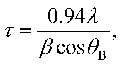 | (1) |
The wavelength-dependent optical absorption properties of the samples were obtained using illumination from a Xe lamp (Model 66902, Newport). Two spectrometers (USB 2000+ and Flame-NIR, Ocean Optics) were used to measure the incident, transmitted and reflected light at UV-visible and near-infrared regions, respectively. Bi2S3 thin films were prepared on quartz slides (1 mm thick, Ted Pella) for the optical measurements to minimize diffuse scattering by FTO substrates. For both the transmission and reflection measurements, light was incident at a 45° angle to the back-side (quartz) surface of the sample. For the transmission measurements, the spectrometers were aligned with the incident light to capture the transmitted light (T). For the reflection measurements, the spectrometers were placed at a 90° angle to the incident light to capture the reflected light (R). The absorption efficiency was calculated using
| A(λ) = 100% − T(λ) − R(λ). | (2) |
The light absorption depth (δ) was then calculated as
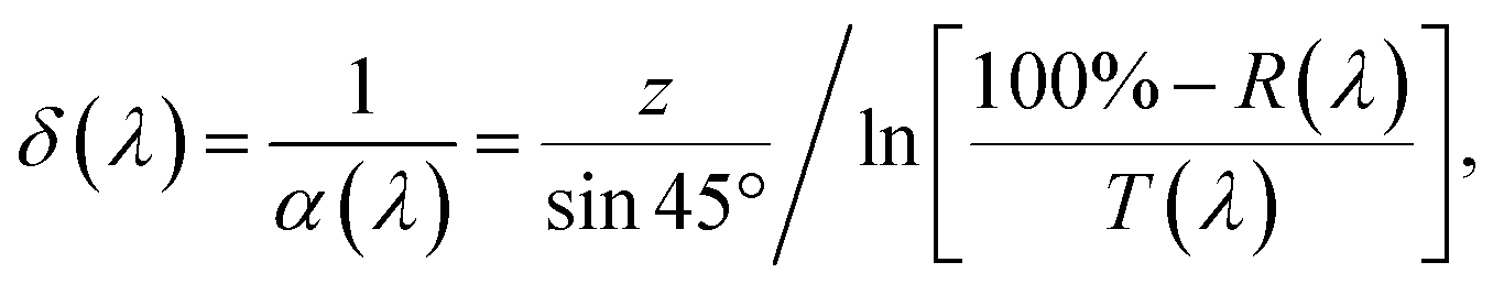 | (3) |
A PHI5600 XPS system acquired all photoelectron spectra. The instrument utilized a monochromated Kα Al source and a third-party data acquisition system (RBD Instruments, Bend Oregon). Analysis chamber base pressures were <1 × 10⁻⁹ torr. A hemispherical energy analyzer that was positioned at 90° with respect to the incoming X-ray flux and 45° with respect to standard sample positioning collected the photoelectrons. High-resolution XP spectra employed a 23.5 eV pass energy, 25 meV step size, and a 50 ms dwell time per step. High-resolution spectra quantified Bi 4f, S 2s (due to the spectral overlap and difficulty in resolving S 2p from Bi 4f), O 1s, and C 1s regions of the photoelectron spectrum. The XPS spectra were calibrated based on a binding energy of 284.8 eV for adventitious carbon. Post-acquisition data fitting of the spectral features utilized a Shirley-shaped background and GL(70) functional peak shapes for Bi 4f spectra while fits to the S 2s region utilized a linear background and GL(30) functional peak shapes.20,21 The Bi 4f doublets were assigned identical full width at half maximum (FWHM) peak widths with areas for 4f5/2 peaks containing 75% of the area of 4f7/2 peaks.22 To prevent mathematically optimized but physically unrealistic peak widths, all features in the S 2s spectral region were constrained to identical FWHM values.
The photoconductivity and photoexcited carrier lifetime were analyzed using the TRTS technique. The charge carriers were excited in the sample with an ultrafast optical pump pulse with photon energy above the band gap, and the transient photoinduced conductivity was monitored in transmission using a time-delayed THz pulse. Here we used 100 fs duration, 400 nm pulses derived from a 1 kHz amplified Ti:sapphire laser source for excitation. Absorption of both un-annealed and S-annealed Bi2S3 films was similarly high at 400 nm. Thus, comparing transient photoconductive response at this excitation wavelength allows us to focus exclusively on the effect of annealing on microscopic conductivity and carrier lifetime. THz probe pulses were generated by optical rectification of 800 nm, 100 fs pulses from the same laser source in a [110] ZnTe crystal, and coherently detected by free-space electro-optic sampling in a second [110] ZnTe crystal.
The PEC measurements were performed in a three-electrode configuration, using a potentiostat (Model SP-200, BioLogic) under back-side broadband illumination from a Xe lamp. The incident light intensity from the Xe lamp at each wavelength was measured by a spectrometer. The integrated power of the Xe lamp output at wavelengths shorter than 950 nm (1.3 eV) was 81.7 mW cm−2, as compared to 71.0 mW cm−2 for the standard AM 1.5G spectrum (Fig. S1a†). Current density–voltage curves (J–V curves) were measured at a scan rate of 10 mV s−1. J–V curves in aqueous electrolytes were measured in a three-electrode configuration with the Bi2S3 photoanode as the working electrode, a Pt wire (0.5 mm diameter, 99.99%, Sigma Aldrich) as the counter electrode, and a saturated calomel (SCE) reference electrode (Gamry). The aqueous electrolyte used was 0.3 M Na2S electrolyte (pH ≈ 13). Potentials (in volts) in aqueous electrolytes are reported versus the reversible hydrogen electrode (RHE) using
| VRHE = VSCE + 0.244 + [0.059 × pH]. | (4) |
The light absorption efficiency (ηabs) is the fraction of incident photons that are absorbed. The charge separation efficiency (ηsep) is the fraction of absorbed photons that reach the semiconductor/electrolyte interface. The product of light absorption efficiency (ηabs) and charge separation efficiency (ηsep) was calculated at each potential V by
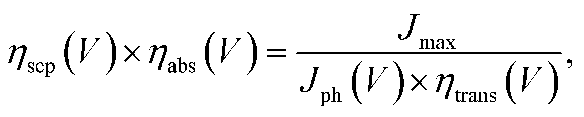 | (5) |
The incident photon-to-current efficiency (IPCE), also known as external quantum efficiency (EQE), was measured at 0.6 VRHE, which is the onset potential for sulfide oxidation in the dark. A Xe lamp equipped with a monochromator (Cornerstone 130 1/8 m, Newport) was used as the illumination source. The spectral irradiance of monochromatic light at each wavelength was measured by a spectrometer and reported in Fig. S1b.† The IPCE was calculated using
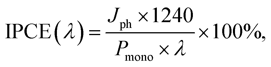 | (6) |
 | (7) |
Density functional theory (DFT) calculations were implemented by the Vienna ab initio simulation package (VASP) code.23,24 We used the generalized gradient approximation (GGA) exchange and correlation functionals as parameterized by Perdew, Burke, and Ernzerhof (the PBE functional).25,26 The electron–ion interactions were treated within the framework of the standard frozen-core projector augmented-wave (PAW) method with valence configurations of 6s26p35d10 for Bi and 3s23p4 for S.27,28 An energy cut-off of 400 eV was used in the plane-wave basis-set expansion. Gaussian smearing with a width of 0.2 eV was used for ionic relaxation and the tetrahedron method with Blöchl corrections was used for density of states (DOS) calculations. The Grimme D3 correction method was used to account for dispersion interactions between layers of Bi2S3.29 For calculations of the pristine Bi2S3 bulk unit cell (1 × 1 × 1), a 6 × 2 × 2 Monkhorst–Pack30k-point sampling was used for ionic relaxation. For defect calculations, a bulk supercell (3 × 1 × 1) containing 60 atoms was constructed and spin-polarized DFT calculations were performed (Fig. S2†). For calculations of the bulk supercell, a 2 × 2 × 2 k-point sampling was used for ionic relaxation and a higher 8 × 8 × 8 k-point sampling was used for density of states calculations. Electronic band structure calculations were performed with 50 k-points in each high symmetry direction within reciprocal space of the crystal. Defect formation energies were calculated by
| ΔEdefective = Edefective − Estoichiometric + ∑ndefectμdefect, | (8) |
Results and discussion
Both the un-annealed and sulfur-annealed Bi2S3 films were ∼150 nm thick (Fig. 1a and b). The crystallite size of the un-annealed Bi2S3 nanocrystals was measured to be ∼10 nm by TEM (Fig. 1c). Because of the small size of the Bi2S3 nanocrystals, the XRD pattern of the un-annealed Bi2S3 film (Fig. 1d) shows peaks only from the underlying FTO substrate, and no peaks indexed to Bi2S3. This is in contrast to a previous report, in which XRD peaks from a NaBiS2 impurity phase were observed in the Bi2S3 synthesized by SILAR from saturated precursor solutions at 80 °C.13 On the other hand, annealing the solution-deposited Bi2S3 film in sulfur vapor at 445 °C results in a XRD pattern with peaks that can be indexed to pure orthorhombic Bi2S3 (ICDD PDF 04-014-6675) (Fig. 1d). The average crystallite size of the S-annealed Bi2S3 film was calculated to be ∼45 nm from the (112) reflections of the XRD pattern, and SEM micrographs show that the S-annealed film contains Bi2S3 grains with an average diameter that is very similar to this average crystallite size (Fig. 1b). Therefore, sulfur vapor annealing increases the crystallite size of the solution-deposited Bi2S3 from ∼10 nm to ∼45 nm.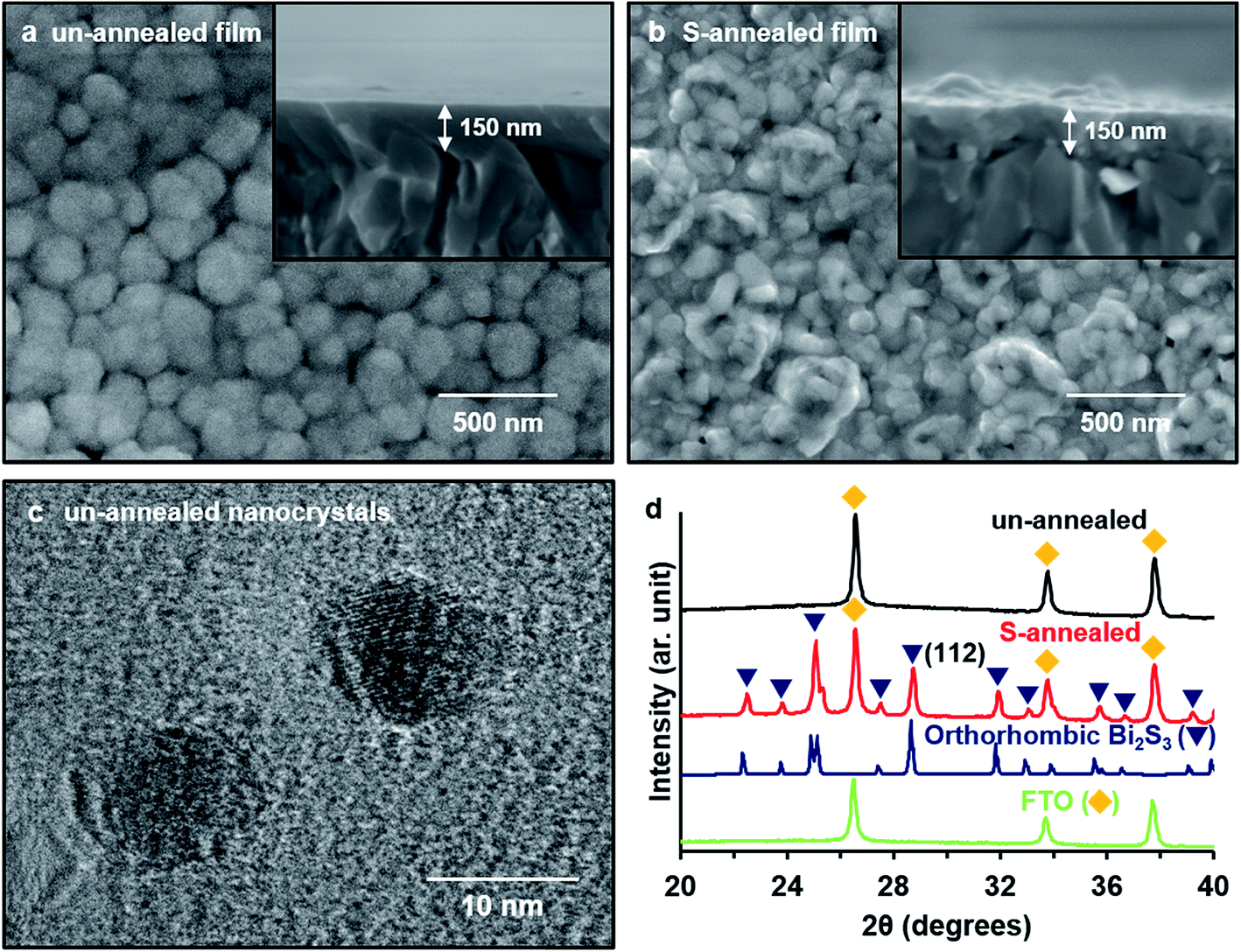 | ||
| Fig. 1 Top-view and cross-section SEM images of 10 layers of (a) un-annealed and (b) S-annealed Bi2S3 thin films on FTO substrate. (c) TEM image of un-annealed Bi2S3 nanocrystals. The background is the amorphous carbon film of the TEM grid. (d) XRD patterns of un-annealed and S-annealed Bi2S3 thin films. | ||
The light absorption efficiency of the Bi2S3 thin film significantly increases at longer wavelengths after sulfur vapor annealing (Fig. 2a). From the measured optical absorption spectra, the indirect band gaps can be determined from the (αhν)1/2vs. hν Tauc plot (Fig. 2b). The S-annealed Bi2S3 was thus determined to possess an indirect band gap of ∼1.24 eV. The experimentally determined band gap corresponds well to the theoretically predicted fundamental band gap, which is found to be indirect and occurs in the ΓX region of the Brillouin zone,32 with energy of 1.25 eV (Fig. 2c). However, the un-annealed Bi2S3 appears to have a larger band gap of ∼1.37 eV, which may be due to quantum confinement caused by nanoscale grain size. The S-annealed Bi2S3 has higher absorption at longer wavelengths (red-shifted) due to the increased crystallite size and lack of quantum confinement. The sub-bandgap absorption of the un-annealed Bi2S3 reaches a minimum value of ∼2.6% at 950 nm (1.31 eV), which suggests that the diffuse scattering by quartz substrate is negligible. Moderate sub-bandgap absorption is observed for the S-annealed Bi2S3, which is attributed to electronic transitions from the defects states to the conduction band, as will be discussed later along with IPCE. Overall, the S-annealed films absorb 67.0% of above-gap photons, compared to only 50.1% for the un-annealed films, despite the films having nearly identical thickness.
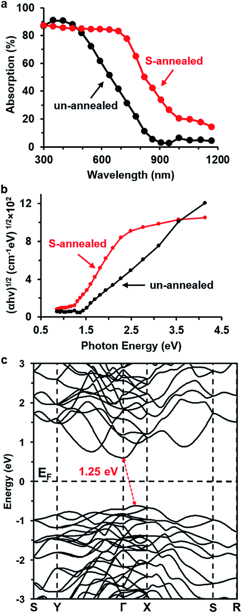 | ||
| Fig. 2 (a) Optical absorption efficiencies. (b) Tauc plots to determine the indirect band gaps of 10 layers of un-annealed and S-annealed Bi2S3 thin films. (c) DFT electronic band structure of pristine Bi2S3. | ||
X-ray photoelectron spectroscopy was used to quantify the chemical compositions of both un-annealed and S-annealed Bi2S3 films. Fig. 3 reports the XP spectra for the (a) Bi 4f and S 2p regions and the (b) S 2s region of the photoelectron spectra both for (top) un-annealed and for (bottom) S-annealed Bi2S3 films. Prior studies ascribed peaks at 158.9 eV to the Bi 4f7/2 feature from Bi2S3 and 159.3 eV to the corresponding feature from Bi2O3.33 For the Bi 4f region of the un-annealed film (Fig. 3a, top), fits reveal a feature at 158.6 eV (red) and a feature at 159.4 eV (blue). In agreement with prior studies, we ascribe the fit of the red doublet to Bi2S3 and the fit of the blue doublet to Bi2O3 in both the un-annealed and sulfur-annealed Bi 4f spectra. Notably, both Bi2S3 and a large amount of Bi2O3 are present on the surface of the un-annealed Bi2S3, which we interpret to indicate film oxidation either during the solution deposition process or by exposure to the air ambient. For the S 2s region of the un-annealed film (Fig. 3b, top), fits are dominated by a feature at 225.8 eV (red) that we attribute to S2− in the Bi2S3. Additionally, the S 2s spectrum for the un-annealed film contains a smaller feature at 228.1 eV (green) that we attribute to neutral sulfur and two features above 231 eV (blue) that we attribute to highly oxidized sulfur species, denoted SOx. The spectra at the bottom of Fig. 3 show each respective region following the sulfur annealing. The Bi 4f region of the S-annealed film (Fig. 3a, bottom) demonstrates significantly smaller Bi 4f features due to bismuth oxide as compared to the oxide features in the un-annealed film. Concomitant with the sulfur treatment, the S 2s region in the bottom of Fig. 3b demonstrates higher concentrations of the neutral sulfur (S0) relative to the un-annealed film. We attribute the excess S0 feature to trace sulfur from the annealing process that may be incorporated as interstitial sulfur in the Bi2S3 crystal and/or residual surface sulfur. Interestingly, the sulfur annealing step did not attenuate the SOx features (blue) relative to the un-annealed film.
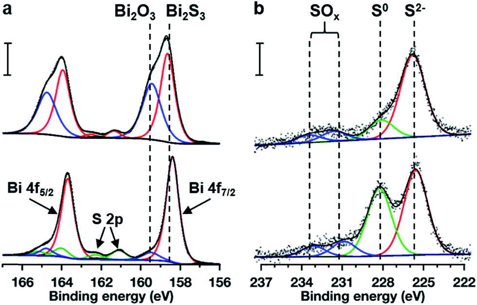 | ||
| Fig. 3 X-ray photoelectron spectra of Bi2S3 thin films without annealing (top) and with sulfur vapor annealing at 445 °C (bottom). (a) Bi 4f and S 2p XP spectra and (b) S 2s XP spectra. Red traces correspond to fitted peaks ascribed to Bi2S3 for both the Bi 4f and S 2s spectral regions. Blue traces represent fitted peaks ascribed to oxidized species Bi2O3 and highly oxidized sulfur, denoted SOx. Comparing the spectra of the un-annealed sample to the sulfur-annealed sample, the sulfur annealing dramatically decreased the quantity of bismuth oxide at the surface. However, the sulfur annealing did not remove oxidized sulfur species and somewhat increased the concentration of neutral sulfur species (green). The scale bar represents 2000 counts per second for the Bi 4f and S 2p spectra and 450 counts per second for S 2s. | ||
The influence of defects on the electronic structure was then analyzed by calculating the DOS of pristine and defect-containing Bi2S3, along with their formation energies (Fig. 4 and S3†). We hypothesize that the sulfur vapor annealing fills in sulfur vacancies of the un-annealed Bi2S3. The defect states related to a sulfur vacancy (Sv) are occupied electronic states found deep in the band gap, at 0.63 eV above the valence band maximum (VBM). This finding is consistent with previous reports that Sv creates deep hole trapping states that allow electron–hole recombination.34–37 Additionally, Bi2S3 containing two Sv possesses a higher DOS population for the mid-gap charge trapping states, which further shows that Sv in Bi2S3 can act as recombination sites (Fig. 4). Therefore, the un-annealed Bi2S3 may contain a higher concentration of mid-gap Sv states, which increases recombination and decreases photoexcited carrier lifetime. Moreover, the S-annealed Bi2S3 likely contains more sulfur interstitials (Si) due to the low formation energy of this defect in a S-rich environment,36 which is consistent with the greater amount of elemental sulfur species observed on the surface of the film by XPS. However, Si only creates shallow hole trapping states that are about 0.12 eV above the VBM. In contrast to the Sv defect states, the trapped holes at Si are less likely to recombine with the photoexcited electrons due to the smaller energy required to remove the holes to the valence band and avoid recombination (Fig. 4). On the other hand, the un-annealed Bi2S3 likely contains more oxygen impurities in the forms of oxygen substituting for sulfur (OS) and oxygen interstitial (Oi), the formation of which is thermodynamically favorable due to the negative formation energies, −0.93 and −0.57 eV, respectively (Fig. S3†). OS–Bi2S3 exhibits similar electronic structure to pristine Bi2S3. This is expected, since oxygen has the same number of valence electrons as sulfur and is more electronegative. Oi–Bi2S3 has a similar DOS to Si–Bi2S3, resulting in shallow electronic states 0.12 eV above the VBM. Therefore, the oxide impurities in the un-annealed Bi2S3 seem to only cause shallow defect states, which may not contribute to the poor performance of the film.
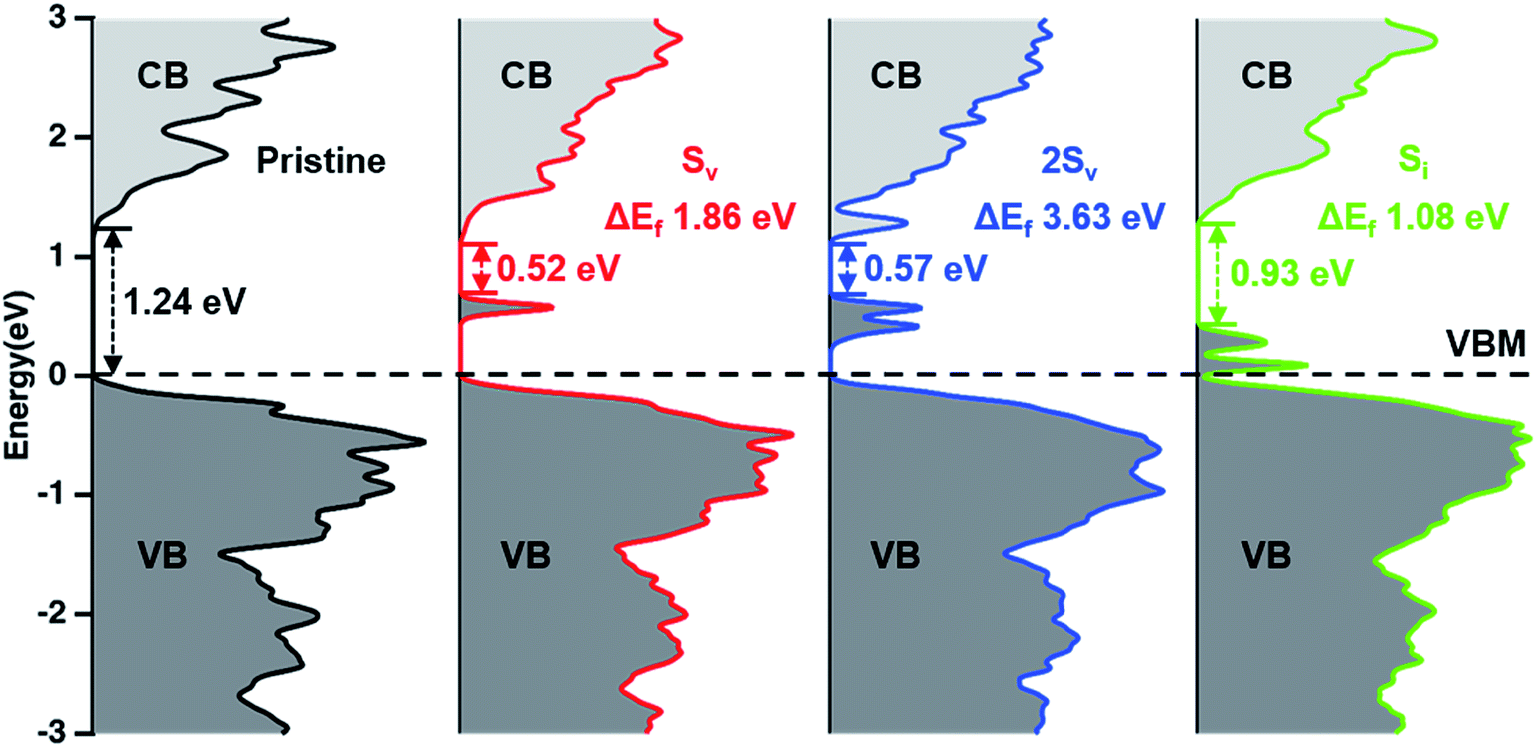 | ||
| Fig. 4 DFT-calculated density of states (DOS) and formation energies of pristine Bi2S3 and Bi2S3 containing sulfur vacancy (Sv), two sulfur vacancies (2Sv), and sulfur interstitial (Si). Dark grey regions show the occupied electronic states, while light grey regions show the unoccupied electronic states. The valence band maximum (VBM) energy is set to zero eV, and is defined as the highest occupied non-defect state. | ||
We then analyzed the impact of sulfur annealing on photoconductivity and photoexcited carrier lifetime using TRTS. We interrogated the pump-induced changes in the sample conductivity with sub-picosecond time resolution by varying the delay between the pump pulse and THz probe pulse. The change in transmission of the main peak of the THz probe pulse, –ΔT/T, as a function of time after excitation with 378 μJ cm−2 pulse, for both un-annealed and S-annealed films is shown in Fig. 5a. It is proportional to the transient photoconductivity.38–40 At the same excitation conditions, peak photoinduced conductivity is more than twice higher in the S-annealed film as a result of a less prevalent fast trapping and recombination of photoinjected charge carriers on a timescale that is shorter than our instrumental response time of ∼300 fs. Moreover, photoconductivity of un-annealed film is very short-lived and decays on sub-picosecond time scale due to both rapid carrier recombination inside the small Bi2S3 crystallites and fast trapping of photoexcited carriers in trap states at crystallite boundaries. Larger grain size, lower concentration of sulfur vacancies, and reduced number of interface defects in S-annealed Bi2S3 film translates into a significantly longer lifetime of mobile carriers (Fig. 5a). Photoconductivity in the S-annealed sample follows a bi-exponential decay with a fast (∼3 ps) and a slower (30 ps) component. The fast decay time is dependent on excitation fluence, increasing from 2.6 ps to 4.4 ps as excitation is decreased 6-fold to 63 μJ cm−2 (Fig. S4†). This suggests that the process responsible for this fast photoconductivity decay is recombination of mobile carriers. On the other hand, the slower, 30 ps component is fluence-independent and represents trapping of carriers at sulfur vacancies and interface states that do not become saturated in the studied fluence range.
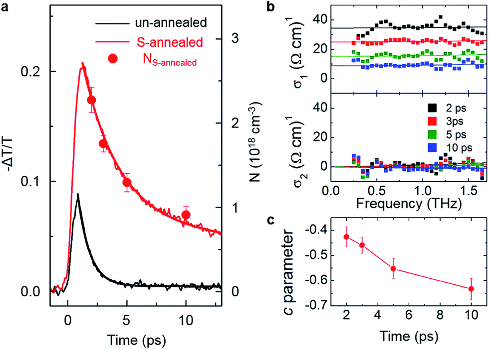 | ||
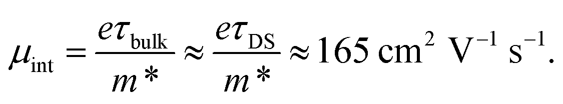
| Fig. 5 Time-resolved THz spectroscopy of un-annealed and S-annealed Bi2S3 thin films. (a) Transient photoconductivity (lines) and instantaneous photoexcited carrier density (symbols) for S-annealed film. Smooth lines represent fits of experimental transient photoconductivity to single- (un-annealed) and bi-exponential (S-annealed film) decays. (b) Real and imaginary components of transient photoconductivity at different times after optical excitation for S-annealed film. Symbols represent experimental data, and lines – fits of experimental data to the Drude–Smith conductivity. (c) Drude–Smith c parameter for S-annealed film. | ||
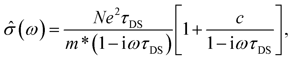
Fixing the pump-probe delay, and detecting the pump-induced changes in the amplitude and phase of the THz pulse transmitted through the sample allows us to extract the complex-valued, frequency-resolved THz photoconductivity spectrum at a given time following the photoexcitation. Fig. 5b shows the real (σ1) and imaginary (σ2) conductivity of the S-annealed Bi2S3 film at 2, 3, 5 and 10 ps after excitation with a 378 μJ cm−2 pulse. The real component of conductivity decreases with time while the imaginary one stays almost unchanged and close to zero. We analyze this progression by fitting both real and imaginary conductivity to the Drude–Smith model, a phenomenological model of microscopic THz conductivity in granular materials where the grain size is comparable to the carrier mean free path.38,41–48 It allows the extraction of the instantaneous photoexcited carrier density N, the effective scattering time τDS, and a measure of carrier localization within individual grains at a given time after excitation:
 | (9) |
| 1/τDS = 1/τbulk + 1/τboundary. | (10) |
Lines in Fig. 5b are Drude–Smith fits to the experimental complex conductivity. The resulting carrier density is plotted as circles in Fig. 5a, and it follows the same trend as the bi-exponential decay of photoconductivity, indicating that trapping and recombination of mobile carriers is responsible for the observed transient reduction in photoconductivity while the intrinsic carrier mobility stays unchanged. Effective carrier scattering time τDS is unchanged over the first 10 ps and equal to 23 ± 5 fs, corresponding to the carrier mean free path of ∼3 nm. As the mean free path is significantly smaller than the ∼45 nm average grain size, contribution of grain boundary scattering to the effective relaxation time is negligible, and intrinsic, intra-grain mobility (μint) can be estimated as
 | (11) |
However, long-range, inter-grain mobility decreases as carriers, while free to move within the individual grains, becomes more localized inside those grains. This phenomenon is reflected in the time dependence of the c parameter, which changes from ∼−0.43 ± 0.04 at 2 ps to −0.63 ± 0.04 at 10 ps after excitation, as has been observed in other polycrystalline systems.38,43 There are two possible explanations for this behavior, which we are not presently able to distinguish between. One possibility is that, as carriers get trapped at inter-grain boundaries, the electrostatic field associated with those carriers increases the height of the potential barrier experienced by the free carriers.51 Another possible explanation is that the semiconductor goes towards a flat-band condition under illumination due to the large concentration of photoexcited carriers, resulting in a decrease in an already-existing potential barrier at the grain boundaries, and that this potential barrier subsequently returns to its original height as the photoexcited carriers recombine.52 Regardless of the mechanism, the long-range, dc-mobility of the film, μdc = (1 + c)μint decreases as a function of time after excitation from 111 cm2 V−1 s−1 at 2 ps to 61 cm2 V−1 s−1 at 10 ps. Based on a carrier lifetime (t) of 30 ps and an inter-grain mobility (μdc) of 61 cm2 V−1 s−1, the carrier diffusion length (LD) can be calculated as
 | (12) |
This carrier diffusion length is similar to the light absorption depth at ∼700 nm (Fig. S5†), which suggests that simultaneously high light absorption and charge separation efficiencies can be achieved in the S-annealed Bi2S3 thin films, leading to high overall solar energy conversion efficiencies.53 On the other hand, for un-annealed Bi2S3 films, low signal/noise ratio in the complex conductivity spectra did not permit accurate measurement of mobility.
The solar energy conversion efficiency of the 10 layers of Bi2S3 thin films with and without sulfur vapor annealing at 445 °C was evaluated by photoelectrochemical (PEC) measurements of the wavelength-dependent photon-to-current efficiencies and the potential-dependent light absorption and charge separation efficiencies (Fig. 6). The film thickness and annealing temperature were optimized for maximum photocurrent under white light illumination (Fig. S6†). The IPCE of the S-annealed films reaches a plateau of ∼40% at short wavelengths, compared to a plateau of ∼5% for the un-annealed films, and is higher than that of the un-annealed films at all wavelengths (Fig. 6a). The IPCE of the S-annealed films shows a sharp rise at wavelengths shorter than 1000 nm, which is consistent with the measured band gap of 1.25 eV, while the IPCE of the un-annealed films show a rise at wavelength shorter than 900 nm, which is consistent with the measured band gap of 1.37 eV. As mentioned earlier, the smaller band gap of the S-annealed Bi2S3 is consistent with the larger grain size of the films and a resulting lack of quantum confinement. In addition, IPCE shows sub-bandgap photon-to-current conversion up to 1100 nm for the S-annealed Bi2S3 film and up to 1050 nm for the un-annealed Bi2S3. The sub-bandgap IPCE for the un-annealed Bi2S3 is likely attributed to the electronic transition from the Oi defect states to the CBM (1.10 eV; see Fig. S3†) due to the expected abundance of Oi in the un-annealed film. The sub-bandgap IPCE for the S-annealed Bi2S3 is likely due to transition from the Si defect states to the CBM (0.93 eV; see Fig. 4) due to the large amount of Si expected in the film. Moreover, the APCE of the S-annealed films reaches a value of ∼50% at short wavelengths, compared to a maximum value of ∼15% for the un-annealed films, and is higher than that of the un-annealed films at all wavelengths (Fig. 6b). It should be noted that the measured quantum efficiencies do not represent the optimum performance of the Bi2S3 thin films as the applied voltage is lower than the built-in voltage that could be achieved in a photovoltaic device.11 Additionally, the product of ηabs and ηsep is calculated from the J–V curves under white-light illumination (Fig. 6c), and reaches a value of ∼35% for the S-annealed films but only ∼5% for un-annealed films at 1 VRHE. At the same voltage, ηsep (Fig. 6d) reaches a value of ∼55% for the S-annealed films, but only ∼10% for un-annealed films. The enhanced quantum efficiency and charge separation efficiency after sulfur annealing can be explained by an increased photoexcited carrier lifetime, consistent with the results of the THz spectroscopy characterization. Although the charge-carrier mobility was measured by THz spectroscopy only for the S-annealed films, it is very likely that the mobility is also higher than that for un-annealed films, further explaining the increased performance.
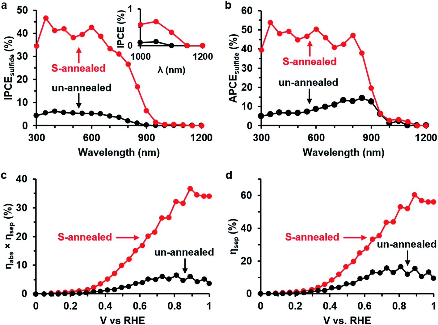 | ||
| Fig. 6 (a) IPCE and (b) APCE of 10 layers of un-annealed and S-annealed Bi2S3 thin films measured at 0.6 VRHE in 0.3 M Na2S aqueous electrolyte at pH 13. (c) Products of ηabs and ηsep, and (d) ηsep of 10 layers of un-annealed and S-annealed Bi2S3 thin films at different potentials measured in 0.3 M Na2S aqueous electrolyte. | ||
The Bi2S3 thin films exhibit n-type conductivity according to these PEC measurements, which is consistent with other reports.6,9,12 The n-type conductivity of Bi2S3 has been attributed to the presence of Sv and Si donor defects.36 However, for defect states to behave as effective donor levels, the energy difference between the defect states and the conduction band minimum (CBM) should be comparable to the thermal energy at room temperature (0.026 eV). Therefore, Sv and Si defect states, which have energies that are 0.52 and 0.93 eV below the CBM, respectively, cannot act as effective donor levels, and cannot be responsible for the n-type conductivity of Bi2S3. We additionally calculated the formation energies and density of states for Bi2S3 containing hydrogen substituted for sulfur (HS), or hydrogen interstitials (Hi). The DOS of HS and Hi– Bi2S3 (Fig. 7) show occupied states within the conduction band of Bi2S3, which suggests that these hydrogen impurities can create effective donor levels in Bi2S3 without introducing mid-gap charge trapping states. In fact, hydrogen impurities have previously been to found to cause the n-type conductivity of other semiconductors, such as BiVO4.54 Moreover, the formation energy of Hi is negative and the formation energy of HS is smaller than those of Sv and Si, which indicates that the incorporation of hydrogen is energetically favorable. Hydrogen may be incorporated into Bi2S3via the decomposition of precursors during the solution deposition process and/or from water vapor in the annealing environment. Although this requires further investigation, we propose that hydrogen impurities may play a role in causing the n-type conductivity of Bi2S3.
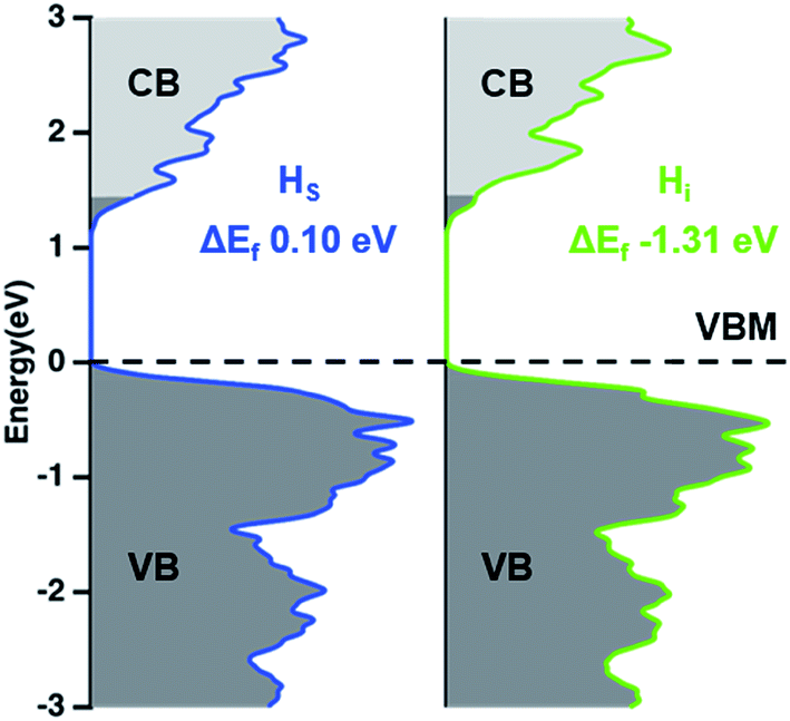 | ||
| Fig. 7 DFT-calculated density of states (DOS) and formation energies of Bi2S3 containing hydrogen substitution of sulfur (HS) and hydrogen interstitial (Hi). | ||
Conclusions
We have synthesized Bi2S3 thin film photoelectrode via a combination of solution deposition and sulfur vapor annealing. We have identified three major advantages of the annealing process. First, the sulfur vapor annealing improves crystallinity of the solution-deposited Bi2S3 nanocrystals by increasing the crystallite size from ∼10 nm to ∼45 nm. Second, sulfur vapor annealing converts the surface oxides of the un-annealed film to sulfides and thus improves the purity of the film. Third, sulfur vapor annealing may fill in sulfur vacancies of the un-annealed Bi2S3 to significantly reduce the concentration of mid-gap charge recombination sites, resulting in longer photoexcited carrier lifetimes and higher internal quantum efficiencies. Overall, the S-annealed Bi2S3 achieves carrier diffusion lengths that are comparable to the light absorption depth, which makes it promising for photovoltaic and photoelectrochemical energy conversion applications. The sulfur vapor annealing method could be utilized as a general approach to enhance the optoelectronic performance of solution-deposited metal sulfide materials. Moreover, DFT calculations show that hydrogen doping creates effective donor levels at the conduction band edge of Bi2S3, which should increase electron conductivity without introducing recombination sites. This direction can be explored in future experimental work.Author contributions
Z. Z. and P. M. R. conceived the study. Z. Z. carried out the thin film synthesis, optical and PEC measurements, DFT calculations, XRD and XPS characterizations. S. K. I. and N. A. D. advised on the DFT calculations. K. K. and L. V. T. performed the TRTS characterization. A. D. C. and R. L. G. assisted with the XPS characterization. L. Z. performed the SEM and TEM characterizations. D. R. B. contributed to the design and interpretation of the experiments and simulations. Z. Z., R. L. G., L. V. T., N. A. D. and P. M. R. wrote the manuscript. All authors discussed the results and revised the manuscript.Conflicts of interest
There are no conflicts to declare.Acknowledgements
Z. Z. acknowledges support from the WPI Summer Undergraduate Research Fellowship (SURF).References
- N. S. Lewis, Toward Cost-Effective Solar Energy Use, Science, 2007, 315(5813), 798–801 CrossRef CAS PubMed.
- A. A. Tahir, M. A. Ehsan, M. Mazhar, K. G. U. Wijayantha, M. Zeller and A. D. Hunter, Photoelectrochemical and Photoresponsive Properties of Bi2S3 Nanotube and Nanoparticle Thin Films, Chem. Mater., 2010, 22(17), 5084–5092 CrossRef CAS.
- H. He, S. P. Berglund, P. Xiao, W. D. Chemelewski, Y. Zhang and C. B. Mullins, Nanostructured Bi2S3/WO3 heterojunction films exhibiting enhanced photoelectrochemical performance, J. Mater. Chem. A, 2013, 1(41), 12826–12834 CAS.
- Y.-C. Lin and M.-W. Lee, Bi2S3 Liquid-Junction Semiconductor-Sensitized SnO2 Solar Cells, J. Electrochem. Soc., 2014, 161(1), H1–H5 CrossRef CAS.
- Q. Zeng, J. Bai, J. Li, Y. Li, X. Li and B. Zhou, Combined nanostructured Bi2S3/TNA photoanode and Pt/SiPVC photocathode for efficient self-biasing photoelectrochemical hydrogen and electricity generation, Nano Energy, 2014, 9, 152–160 CrossRef CAS.
- G. Ai, R. Mo, Q. Chen, H. Xu, S. Yang, H. Li and J. Zhong, TiO2/Bi2S3 core-shell nanowire arrays for photoelectrochemical hydrogen generation, RSC Adv., 2015, 5(18), 13544–13549 RSC.
- Y. Cao, M. Bernechea, A. Maclachlan, V. Zardetto, M. Creatore, S. A. Haque and G. Konstantatos, Solution Processed Bismuth Sulfide Nanowire Array Core/Silver Sulfide Shell Solar Cells, Chem. Mater., 2015, 27(10), 3700–3706 CrossRef CAS.
- C. Liu, J. Li, Y. Li, W. Li, Y. Yang and Q. Chen, Epitaxial growth of Bi2S3 nanowires on BiVO4 nanostructures for enhancing photoelectrochemical performance, RSC Adv., 2015, 5(88), 71692–71698 RSC.
- C. Liu, Y. Yang, W. Li, J. Li, Y. Li, Q. Shi and Q. Chen, Highly Efficient Photoelectrochemical Hydrogen Generation Using ZnxBi2S3+x Sensitized Platelike WO3 Photoelectrodes, ACS Appl. Mater. Interfaces, 2015, 7(20), 10763–10770 CAS.
- L. Whittaker-Brooks, J. Gao, A. K. Hailey, C. R. Thomas, N. Yao and Y.-L. Loo, Bi2S3 nanowire networks as electron acceptor layers in solution-processed hybrid solar cells, J. Mater. Chem. C, 2015, 3(11), 2686–2692 RSC.
- M. Han and J. Jia, 3D Bi2S3/TiO2 cross-linked heterostructure: An efficient strategy to improve charge transport and separation for high photoelectrochemical performance, J. Power Sources, 2016, 329, 23–30 CrossRef CAS.
- C. Liu, Y. Yang, W. Li, J. Li, Y. Li and Q. Chen, In situ synthesis of Bi2S3 sensitized WO3 nanoplate arrays with less interfacial defects and enhanced photoelectrochemical performance, Sci. Rep., 2016, 6, 23451 CrossRef CAS PubMed.
- I. Zumeta-Dubé, V.-F. Ruiz-Ruiz, D. Díaz, S. Rodil-Posadas and A. Zeinert, TiO2 Sensitization with Bi2S3 Quantum Dots: The Inconvenience of Sodium Ions in the Deposition Procedure, J. Phys. Chem. C, 2014, 118(22), 11495–11504 Search PubMed.
- H. Bao, C. M. Li, X. Cui, Y. Gan, Q. Song and J. Guo, Synthesis of a Highly Ordered Single-Crystalline Bi2S3 Nanowire Array and its Metal/Semiconductor/Metal Back-to-Back Schottky Diode, Small, 2008, 4(8), 1125–1129 CrossRef CAS PubMed.
- X. S. Peng, G. W. Meng, J. Zhang, L. X. Zhao, X. F. Wang, Y. W. Wang and L. D. Zhang, Electrochemical fabrication of ordered Bi2S3 nanowire arrays, J. Phys. D: Appl. Phys., 2001, 34(22), 3224 CrossRef CAS.
- C. Gao, H. Shen, L. Sun and Z. Shen, Chemical bath deposition of Bi2S3 films by a novel deposition system, Appl. Surf. Sci., 2011, 257(17), 7529–7533 CrossRef CAS.
- A. Hussain, A. Begum and A. Rahman, Effects of annealing on nanocrystalline Bi2S3 thin films prepared by chemical bath deposition, Mater. Sci. Semicond. Process., 2014, 21, 74–81 CrossRef CAS.
- Y. Zhao, K. T. E. Chua, C. K. Gan, J. Zhang, B. Peng, Z. Peng and Q. Xiong, Phonons in Bi2S3 nanostructures: Raman scattering and first-principles studies, Phys. Rev. B: Condens. Matter Mater. Phys., 2011, 84(20), 205330 CrossRef.
- B. D. Cullity and S. R. Stock, Elements of X-ray Diffraction, Prentice Hall, Upper Saddle River, New Jersey 07458, 3rd edn, 2001 Search PubMed.
- N. Fairley, Peak Fitting in XPS2006 05/18/2017 [cited 2017 07/10/2017], http://www.casaxps.com/help_manual/manual_updates/peak_fitting_in_xps.pdf.
- D. A. Shirley, High-Resolution X-Ray Photoemission Spectrum of the Valence Bands of Gold, Phys. Rev. B: Solid State, 1972, 5(12), 4709–4714 CrossRef.
- J. F. Moulder, W. F. Stickle, P. E. Sobol and K. D. Bomben, Handbook of X-ray Photoelectron Spectroscopy: Physical Electronics Division, Perkin-Elmer Corporation, 1993 Search PubMed.
- G. Kresse and J. Furthmüller, Efficient Iterative Schemes for Ab Initio Total-Energy Calculations using a Plane-Wave Basis Set, Phys. Rev. B: Condens. Matter Mater. Phys., 1996, 54(16), 11169–11186 CrossRef CAS.
- G. Kresse and J. Furthmüller, Efficiency of Ab Initio Total Energy Calculations for Metals and Semiconductors using a Plane-Wave Basis Set, Comput. Mater. Sci., 1996, 6(1), 15–50 CrossRef CAS.
- J. P. Perdew, K. Burke and M. Ernzerhof, Generalized Gradient Approximation Made Simple, Phys. Rev. Lett., 1996, 77(18), 3865–3868 CrossRef CAS PubMed.
- J. P. Perdew, J. A. Chevary, S. H. Vosko, K. A. Jackson, M. R. Pederson, D. J. Singh and F. C. Atoms, Molecules, Solids, and Surfaces: Applications of the Generalized Gradient Approximation for Exchange and Correlation, Phys. Rev. B: Condens. Matter Mater. Phys., 1992, 46(11), 6671–6687 CrossRef CAS.
- P. E. Blöchl, Projector Augmented-Wave Method, Phys. Rev. B: Condens. Matter Mater. Phys., 1994, 50(24), 17953–17979 CrossRef.
- G. Kresse and D. Joubert, From Ultrasoft Pseudopotentials to the Projector Augmented-Wave Method, Phys. Rev. B: Condens. Matter Mater. Phys., 1999, 59(3), 1758–1775 CrossRef CAS.
- S. Grimme, J. Antony, S. Ehrlich and H. Krieg, A consistent and accurate ab initio parametrization of density functional dispersion correction (DFT-D) for the 94 elements H-Pu, J. Chem. Phys., 2010, 132(15), 154104 CrossRef PubMed.
- H. J. Monkhorst and J. D. Pack, Special points for Brillouin-zone integrations, Phys. Rev. B: Solid State, 1976, 13(12), 5188–5192 CrossRef.
- K. Momma and F. Izumi, VESTA: a three-dimensional visualization system for electronic and structural analysis, J. Appl. Crystallogr., 2008, 41(3), 653–658 CrossRef CAS.
- H. Koc, H. Ozisik, E. Deligöz, A. M. Mamedov and E. Ozbay, Mechanical, electronic, and optical properties of Bi2S3 and Bi2Se3 compounds: first principle investigations, J. Mol. Model., 2014, 20(4), 2180 CrossRef PubMed.
- W. E. Morgan, W. J. Stec and J. R. Van Wazer, Inner-orbital binding-energy shifts of antimony and bismuth compounds, Inorg. Chem., 1973, 12(4), 953–955 CrossRef CAS.
- M. Aresti, M. Saba, R. Piras, D. Marongiu, G. Mula, F. Quochi, A. Mura, C. Cannas, M. Mureddu, A. Ardu, G. Ennas, V. Calzia, A. Mattoni, A. Musinu and G. Bongiovanni, Colloidal Bi2S3 Nanocrystals: Quantum Size Effects and Midgap States, Adv. Funct. Mater., 2014, 24(22), 3341–3350 CrossRef CAS.
- V. Calzia, R. Piras, A. Ardu, A. Musinu, M. Saba, G. Bongiovanni and A. Mattoni, Atomistic Modeling of Morphology and Electronic Properties of Colloidal Ultrathin Bi2S3 Nanowires, J. Phys. Chem. C, 2015, 119(29), 16913–16919 CAS.
- D. Han, M.-H. Du, C.-M. Dai, D. Sun and S. Chen, Influence of defects and dopants on the photovoltaic performance of Bi2S3: first-principles insights, J. Mater. Chem. A, 2017, 5(13), 6200–6210 CAS.
- S.-Q. Zhan, H. Wan, L. Xu, W.-Q. Huang, G.-F. Huang, J.-P. Long and P. Peng, Native vacancy defects in bismuth sulfide, Int. J. Mod. Phys. B, 2014, 28(23), 1450150 CrossRef.
- L. V. Titova, T. L. Cocker, S. J. Xu, J. M. Baribeau, X. H. Wu, D. J. Lockwood and F. A. Hegmann, Ultrafast carrier dynamics and the role of grain boundaries in polycrystalline silicon thin films grown by molecular beam epitaxy, Semicond. Sci. Technol., 2016, 31(10), 105017 CrossRef.
- L. V. Titova, T. L. Cocker, X. Wang, A. Meldrum and F. A. Hegmann, Ultrafast Carrier Dynamics in Silicon Nanocrystal Films, in Nanoscale Luminescent Materials 2, ECS Transactions, ed. D. J. Lockwood and P. Mascher, 2012, vol. 45, pp. 21–29 Search PubMed.
- J. B. Baxter, C. Richter and C. A. Schmuttenmaer, Ultrafast Carrier Dynamics in Nanostructures for Solar Fuels, Annu. Rev. Phys. Chem., 2014, 65, 423–447 CrossRef CAS PubMed.
- M. C. Beard, G. M. Turner, J. E. Murphy, O. I. Micic, M. C. Hanna, A. J. Nozik and C. A. Schmuttenmaer, Electronic Coupling in InP Nanoparticle Arrays, Nano Lett., 2003, 3(12), 1695–1699 CrossRef CAS.
- J. B. Baxter and C. A. Schmuttenmaer, Conductivity of ZnO Nanowires, Nanoparticles, and Thin Films Using Time-Resolved Terahertz Spectroscopy, J. Phys. Chem. B, 2006, 110(50), 25229–25239 CrossRef CAS PubMed.
- L. V. Titova, T. L. Cocker, D. G. Cooke, X. Wang, A. Meldrum and F. A. Hegmann, Ultrafast percolative transport dynamics in silicon nanocrystal films, Phys. Rev. B: Condens. Matter Mater. Phys., 2011, 83(8), 085403 CrossRef.
- T. L. Cocker, L. V. Titova, S. Fourmaux, G. Holloway, H. C. Bandulet, D. Brassard, J. C. Kieffer, M. A. El Khakani and F. A. Hegmann, Phase diagram of the ultrafast photoinduced insulator-–metal transition in vanadium dioxide, Phys. Rev. B: Condens. Matter Mater. Phys., 2012, 85(15), 155120 CrossRef.
- D. G. Cooke, A. Meldrum and P. Uhd Jepsen, Ultrabroadband terahertz conductivity of Si nanocrystal films, Appl. Phys. Lett., 2012, 101(21), 211107 CrossRef.
- L. V. Titova, T. L. Cocker, X. Wang, A. Meldrum and F. A. Hegmann, (Invited) Ultrafast Carrier Dynamics in Silicon Nanocrystal Films, ECS Trans., 2012, 45(5), 21–29 CrossRef CAS.
- G. W. Guglietta, B. T. Diroll, E. A. Gaulding, J. L. Fordham, S. Li, C. B. Murray and J. B. Baxter, Lifetime, Mobility, and Diffusion of Photoexcited Carriers in Ligand-Exchanged Lead Selenide Nanocrystal Films Measured by Time-Resolved Terahertz Spectroscopy, ACS Nano, 2015, 9(2), 1820–1828 CrossRef CAS PubMed.
- T. L. Cocker, D. Baillie, M. Buruma, L. V. Titova, R. D. Sydora, F. Marsiglio and F. A. Hegmann. Microscopic origin of the Drude-Smith model, arXivorg. 2017.
- D. Guo, C. Hu and C. Zhang, First-principles study on doping and temperature dependence of thermoelectric property of Bi2S3 thermoelectric material, Mater. Res. Bull., 2013, 48(5), 1984–1988 CrossRef CAS.
- G. M. Turner, M. C. Beard and C. A. Schmuttenmaer, Carrier localization and cooling in dye-sensitized nanocrystalline titanium dioxide, J. Phys. Chem. B, 2002, 106(45), 11716–11719 CrossRef CAS.
- L. V. Titova, T. L. Cocker, D. G. Cooke, X. Wang, A. Meldrum and F. A. Hegmann, Ultrafast percolative transport dynamics in silicon nanocrystal films, Phys. Rev. B: Condens. Matter Mater. Phys., 2011, 83(8), 085403 CrossRef.
- R. Beranek, (Photo)electrochemical Methods for the Determination of the Band Edge Positions of TiO2-Based Nanomaterials, Adv. Phys. Chem., 2016, 2016, 2 Search PubMed.
- R. E. Brandt, V. Stevanović, D. S. Ginley and T. Buonassisi, Identifying defect-tolerant semiconductors with high minority-carrier lifetimes: beyond hybrid lead halide perovskites, MRS Commun., 2015, 5(2), 265–275 CrossRef CAS.
- J. K. Cooper, S. B. Scott, Y. Ling, J. Yang, S. Hao, Y. Li, F. M. Toma, M. Stutzmann, K. V. Lakshmi and I. D. Sharp, Role of Hydrogen in Defining the n-Type Character of BiVO4 Photoanodes, Chem. Mater., 2016, 28(16), 5761–5771 CrossRef CAS.
Footnotes |
| † Electronic supplementary information (ESI) available: Spectral output of illumination sources, optimized geometries of defect-containing Bi2S3 supercell, additional results on DOS, TRTS, light absorption, and PEC performance. See DOI: 10.1039/c7se00398f |
| ‡ Present addresses: Department of Materials Science and Engineering, Northwestern University, Evanston, IL 60208, USA. |
| This journal is © The Royal Society of Chemistry 2017 |