
High efficiency quasi 2D lead bromide perovskite solar cells using various barrier molecules†
Bat-El
Cohen
a,
Malgorzata
Wierzbowska
 b and
Lioz
Etgar
*a
b and
Lioz
Etgar
*a
aThe Hebrew University of Jerusalem, Institute of Chemistry, Casali Center for Applied Chemistry, Jerusalem, Israel. E-mail: lioz.etgar@mail.huji.ac.il
bIntitute of High Pressure Physics, Polish Academy of Sciences, ul. Sokolowska 29/37, 01-142 Warsaw, Poland
First published on 10th August 2017
Abstract
This work reports on the high power conversion efficiency (PCE) and high open circuit voltage (Voc) of bromide-based quasi 2D perovskite solar cells. A Voc of more than 1.4 V and, at the same time, a PCE of 9.5% for cells with hole transport material (HTM) were displayed, whereas a Voc value of 1.37 V and a PCE of 7.9% were achieved for HTM-free cells. Bromide quasi 2D perovskites were synthesized using various long organic barriers (e.g., benzyl ammonium, BA; phenylethyl ammonium, PEA; and propyl phenyl ammonium, PPA). The influence of different barrier molecules on the quasi 2D perovskite's properties was studied using absorbance, X-ray diffraction, and scanning electron microscopy. No change was observed in the exciton binding energy as a result of changing the barrier molecule. Density functional theory (DFT) with spin–orbit coupling calculations showed that in the case of BA, holes are delocalized over the whole molecule, whereas for PEA and PPA, they are delocalized more at the phenyl ring. This factor influences the electrical conductivity of holes, which is highest for BA in comparison with the other barriers. In the case of electrons, the energy onset for the nonzero conductivity is lowest for BA. Both calculations support the better PV performance observed for the quasi 2D perovskite based on BA as the barrier. Finally, using contact angle measurements, it was shown that the quasi 2D perovskite is more hydrophobic than the 3D perovskite. Stability measurements showed that cells based on the quasi 2D perovskite are more stable than cells based on the 3D perovskite.
Introduction
In recent years, organic–inorganic halide perovskites have attracted much attention as light absorbing materials for solar cell applications. The commonly used perovskite material in photovoltaic (PV) devices is a three-dimensional (3D) structural framework corresponding to the formula ABX3. For an organic–inorganic halide perovskite, ‘A’ is an organic ammonium cation (usually MA – methylammonium or FA – formamidinium), ‘B’ is a divalent metal (usually Pb or Sn), and ‘X’ is a halogen (Cl, Br, or I). In the 3D perovskite structure, the organic ammonium cations (‘A’) occupy the holes in the inorganic BX62− corner-sharing octahedra. A useful tool for determining the perovskite formation and structure is the Goldschmidt tolerance factor1,2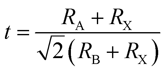 , where RA, RB, and RX are the ionic radii of the corresponding ions (assuming that the individual ions are hard spheres). The perovskite structure can be predicted using a simple geometric consideration; for a 3D perovskite the value of ‘t’ is from 0.8 to 1. A tolerance factor of t ≈ 1 results in the formation of a cubic perovskite structure, whereas lower t values result in a cubic structure of lower symmetry, such as tetragonal or orthorhombic.
Considering the Goldschmidt tolerance factor, the use of a small organic ammonium cation ‘A’ (0.8 ≤ t ≤ 1) forms a 3D perovskite structure, whereas the use of a larger organic ammonium cation ‘R’ (t ≥ 1), which does not fit well inside the octahedral framework, results in a two-dimensional (2D) perovskite (R)2BX4. Mixing both long and short organic ammonium cations results in an interesting class of layered quasi 2D perovskite structures, in which the perovskite octahedra become separated by the long organic ammonium cations forming low-dimensional (R)2(A)n−1BnX3n+1. In this structure, the number of perovskite layers (n) between the organic “barriers” (R) can be varied by controlling the stoichiometry of the components in the perovskite solution (n = ∞ represents 3D perovskites).3 The traditional 3D perovskites exhibit superior electronic properties such as small exciton binding energy and long diffusion length among others, making them promising for PV applications.4–7 On the other hand, 2D perovskites have electronic properties different from their 3D counterparts (such as a high exciton binding energy and a large bandgap),8,9 making it challenging to use them in PV applications.
The use of quasi 2D perovskites as light-absorbing materials in perovskite solar cells (PSCs) was reported in 2014 by Smith et al.10 using (PEA)2(MA)2Pb3I10 perovskite. Although the solar cell performance was poor (an efficiency of 4.7%), the authors predicted future intensive research on quasi 2D perovskites owing to their improved moisture stability. Further studies11–13 on (R-NH3)2MAn−1PbI3n+1 quasi 2D perovskite reported an improvement in the stability of the perovskite to moisture. However, achieving higher efficiencies for quasi 2D perovskite cells comparable to those of 3D perovskite cells remains a challenging task. Sargent et al.11 fabricated quasi 2D perovskites based on planar cells with high n values (n > 40), exhibiting efficiencies comparable to those of 3D perovskite-based cells and with a better stability than the 3D perovskite. A recent study14 reported a hot casting deposition technique that controls the quasi 2D perovskite growth direction in planar PCSs. As a result, a significant power conversion efficiency (PCE) was achieved, approaching 12.5% for (BA)2(MA)3Pb4I13 (BA = butylammonium). Moreover, our recent report15 on quasi 2D perovskites, based on mesoporous cells, indicated that they concomitantly yield high efficiency and high voltage with and without hole transport material.
Bromide based PSCs can potentially be used as a power source in high voltage applications due to the wide bandgap of perovskites (∼2.25 eV). Several studies showed that high open circuit voltage, ranging from 1.15 V to 1.5 V, can be achieved by using 3D bromide based PSCs.16–18 However, the wide band gap of bromide based PSC is limiting the theoretical efficiency that can be produced compare to the iodide based PSC. To the best of our knowledge, the top reported efficiency for MAPbBr3 perovskite based solar cells approaches ∼10% PCE.19
PSCs without the use of the hole transport material (HTM) were first reported in 2012 by Etgar et al.36 In this structure, the perovskite functions as both the light harvesting and hole conducting material, due to the direct contact between the perovskite layer and the metal contact. HTM free PSCs have simple fabrication, improved stability (due to the lack of the organic HTM material) and reduced production costs. HTM free PSCs based on MAPbI3 perovskite currently exhibit more than 11% PCE .20,21
This paper presents a detailed description of bromide-based quasi 2D perovskites (R-NH3)2MAn−1PbBr3n+1 using different ‘R’ barrier groups by studying their influence on the PSC performance. The barrier molecules include benzyl ammonium (BA), phenylethyl ammonium (PEA), and propyl phenyl ammonium (PPA). Absorbance and X-ray diffraction were measured for the 2D perovskite (n = 1) and for the quasi 2D perovskite (n = 50) with various barriers. PSCs with and without HTM were fabricated, resulting in higher open circuit voltage (Voc) and higher PCE compared with the 3D perovskite structure. Theoretical calculations including DFT and spin–orbit coupling provided information on the exciton binding energy, geometrical orientation, charge density maps, band structures, and the electrical conductivity of these quasi 2D perovskites. Finally, stability and contact angle measurements show the superior resistance of these materials to humidity than their counterparts, the 3D perovskite.
Results and discussion
Fig. 1 presents a schematic illustration of the perovskite's dimensionality, starting from one perovskite layer (n = 1) to two perovskite layers (n = 2) until n = ∞, which indicates the 3D perovskite. The films were prepared from solution processed deposition, by dissolving a mixture of precursors in stoichiometric ratios and spin coating it on a substrate, as detailed in the Experimental section. Since the preparation method is solution processed deposition, starting from n > 4, there are mixtures of different perovskite layers in the film;34,35 therefore, it is termed the quasi 2D perovskite. Here, perovskite films corresponding to the formula (R)2(MA)n−1PbnBr3n+1, where R is the organic barrier and MA is methylammonium (CH3NH3+), were synthesized.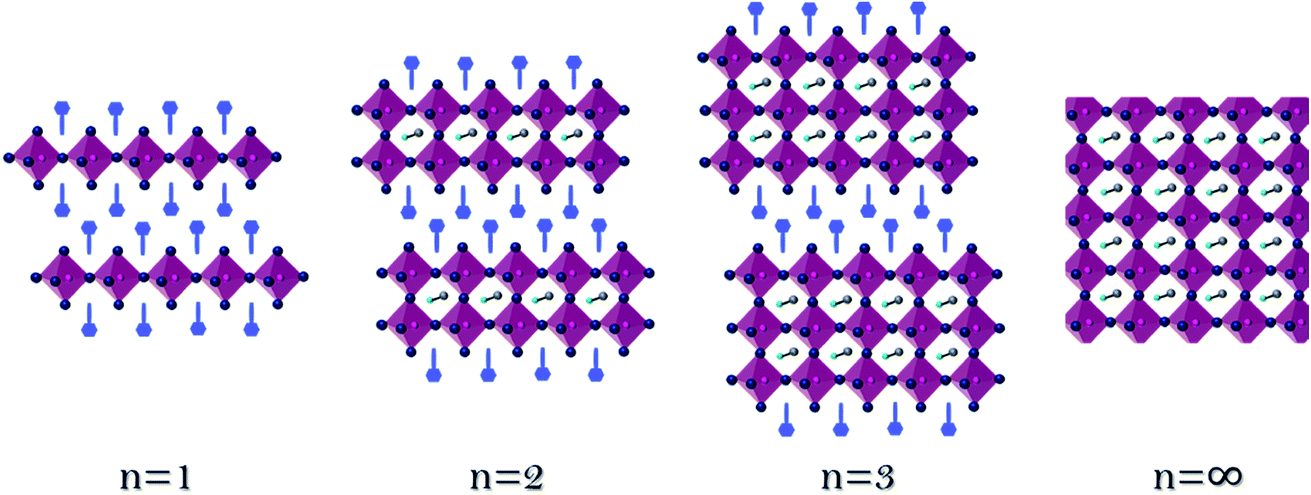 | ||
| Fig. 1 Schematic illustration of the hybrid halide perovskite having the structure (R)2(MA)n−1PbnBr3n+1, where n = 1 corresponds to the 2D halide perovskite R2PbBr4 and n = ∞ corresponds to the 3D perovskite MAPbBr3. | ||
The large organic barrier ‘R’ was changed and its influence on the physical, crystallographic, and photovoltaic properties was investigated. The large organic barrier is responsible for forming the perovskite's dimensionality, as shown in Fig. 1. The studied barriers are presented in Fig. 2, all of which are benzene derivatives that differ in one methylene group, e.g., benzyl ammonium bromide (BABr) (Fig. 2A), phenyl ethyl ammonium bromide (PEABr) (Fig. 2B), and propyl phenyl ammonium bromide (Fig. 2C).
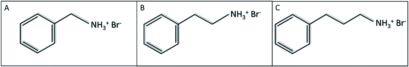 | ||
| Fig. 2 Chemical structures of the different barriers ('R'): (A) benzyl ammonium bromide, (B) phenylethyl ammonium bromide, and (C) propyl phenyl ammonium bromide. | ||
The 2D perovskite structure forms oriented 〈001〉 planes.22Fig. 3A shows the X-ray diffraction (XRD) patterns of the pure 2D perovskite (n = 1, R2PbBr4) for the different barriers (e.g., BABr, PEABr and PPABr) and of the 3D perovskite (n = ∞; MAPbBr3). The XRD pattern of the 2D perovskite exhibits highly ordered peaks, indicating the oriented c-axis of the perovskite. The absence of the peak at 2θ = 15°, which corresponds to the 3D perovskite (MAPbBr3) unit cell, indicates that with all the various barriers, the pure 2D perovskite was formed. The XRD reflection peaks correspond to ‘d’ spacing in the perovskite unit cell; it can be observed that the (BA)2PbBr4 and (PEA)2PbBr4 perovskites have a similar interlayer distance of ∼16.7 Å, whereas (PPA)2PbBr4 has a slightly larger interlayer distance of ∼19.1 Å. The similar interlayer distance of the (BA)2PbBr4 and (PEA)2PbBr4 perovskites may be related to the conformation of the ethyl group in the organic chain.23
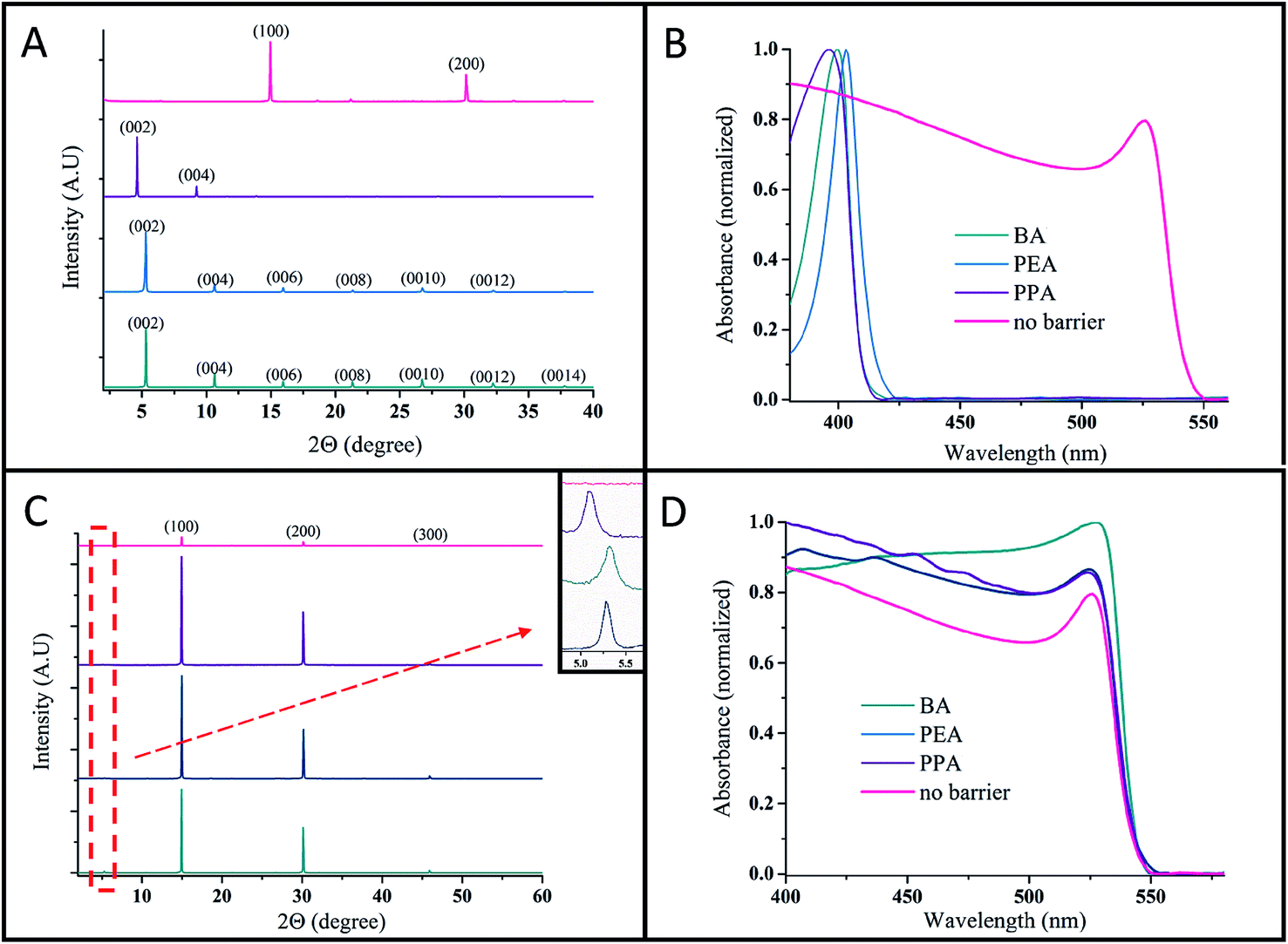 | ||
| Fig. 3 (A) XRD pattern of the 2D perovskite (n = 1) for the different barriers: green – BABr, blue – PEABr, purple – PPABr, and pink – without a barrier (n = ∞). (B) The absorbance spectra for n = 1 and n = ∞ of the different barriers. (C) The XRD patterns for n = 50 and n = ∞ of the various barriers. Inset: magnification of the peaks observed at 2θ ≈ 5.2°. (D) The absorbance spectra for n = 50 and n = ∞ for the different barriers. | ||
Reducing the perovskite dimensionality results in an increased bandgap due to quantum and dielectric confinement. The 2D layered perovskite has a structure with corner-sharing MX62− metal halide octahedra separated by large organic cations that do not fit the perovskite framework; thus, a quantum-well array is formed. In this quantum-well model, the inorganic layers act as a well (forming a high dielectric constant εr ≈ 6) and the organic spacer acts as a barrier (εr ≈ 2).24,25 The dielectric mismatch leads to an “image charge effect” in which the effective coulombic interaction between the electrons and holes in the well increases owing to the lower dielectric constant of the barrier.26,27 Therefore, when the barrier is chemically changed, the exciton binding energy can be tuned.9,25,28 In addition, the bandgap energy increases for low n values due to the same effect (described in more detail below).9,13,15,25 The absorbance spectra of the 2D perovskite (n = 1) with various barriers are presented in Fig. 3B. It can be clearly observed that the bandgap is increased in the 2D perovskite in comparison with the 3D perovskite. It was reported that the organic cations in the high dimensional halide perovskite do not have any significant contribution around the band edge;29 therefore, no change is observed in the energy bandgap between the different barriers, as presented in Fig. 3B for BA, PEA, and PPA. Just a minor change is observed for the PEA barrier; this change can be related to distortion in the inorganic framework, and thus, it indirectly influences the perovskite bandgap.30
Based on our previous work,15 we were motivated to fabricate perovskite solar cells that have approximately 50 layers of perovskite as the so-called quasi 2D halide perovskite. In the case of a few layers of perovskite, the transport properties are not good enough to achieve a high power conversion efficiency. Fig. 3C shows the XRD patterns for n = 50 layers of perovskite using the barriers BA, PEA, PPA, and MAPbBr3 (the 3D perovskite). The change in the unit cell can be detected by XRD; when a single perovskite layer is added, a reflection angle appears below 2θ = 15°, which is the lowest angle detected for the 3D perovskite unit cell.31 The inset of Fig. 3C presents a magnification of the angle 2θ ≈ 5.2°. It is clearly seen that a reflection peak appears in all the samples (n = 50) (which are related to different barriers); however, this peak cannot be detected for n = ∞ (the 3D perovskite), which supports the 2D nature of these samples. Furthermore, optical microscope images of the R2(MA)n−1PbnBr3n+1 (where n = 60 and R = BA/PEA/PPA) and 3D perovskites (n = ∞) are presented in Fig. 1S.† The platelet nature of the layered perovskite with regard to the thick 3D crystals can be clearly detected. The absorbance spectra of the n = 50 layered perovskite with the different barriers are presented in Fig. 3D. The bandgap does not change between the different barriers; this is also related to the 3D perovskite. The exciton absorbance peak, which characterizes the bromide-based perovskite, is observed quite below the bandgap energy when n = 50 (the quasi 2D perovskite) and with the 3D perovskite. Additional absorbance features (related to additional excitonic states) that are assigned to the 2D and quasi 2D perovskites8,9,13 are observed in the absorbance spectra at higher energies. In order to estimate the exciton binding energy for n = 1 and n = 50 for the various barriers, we used the Elliott formula, as presented in Fig. 2S.†32,33 For n = 1, the exciton binding energy (Eb) value was 310–320 meV for the three barriers, whereas for n = 50 the Eb value was 55–56 meV for all barriers. The difference between n = 1 and n = 50 is clearly observed, as was previously discussed. However, no difference in the Eb value was observed between the barriers, as expected.
Following the physical and optical characterizations, we introduced the quasi 2D perovskite into a solar cell structure. First, we investigated the functionality of these materials in the HTM free configuration. The quasi 2D perovskites are from the structure (R-NH3)2(MA)n−1PbnBr3n+1, where the n = 40, 50, and 60 layers were investigated for the different barriers (i.e., BA, PEA, and PPA).
Fig. 3S† shows the cross-sectional HR-SEM of the HTM-free PSCs using the different barriers BA, PEA, and PPA and of the 3D perovskite. In all cases, the perovskite film thickness is around 400 nm, whereas the TiO2 film thickness is ca. 300 nm; the gold back contact can be clearly observed to have a thickness of 70 nm. No change was observed between the different quasi 2D perovskites and the 3D perovskite based on the cross-sectional HR-SEM. However, the cubic nature of the bromide-based perovskite can be observed.
The average photovoltaic (PV) results of the different n values are presented in Tables 1, 1S and 2S† for n = 50, n = 40, and n = 60, respectively. The best average PV performance was achieved with n = 50. Table 1 summarizes the average PV results and Fig. 10S† displays the JV curves of HTM-free PSCs for the quasi 2D perovskite (R)2(MA)49Pb50Br151, (n = 50), where R indicates the barrier, whereas for the 3D perovskite (MAPbBr3), there is no barrier.
| R | V oc (V) | J sc (mA cm−2) | FF (%) | Efficiency (%) |
|---|---|---|---|---|
| No barrier | 1.11 ± 0.06 (1.14) | 8.1 ± 0.6 (9.6) | 58 ± 4 (56) | 5.2 ± 0.6 (6.2) |
| BA | 1.24 ± 0.08 (1.37) | 8.9 ± 0.4 (9.0) | 66 ± 2 (64) | 7.3 ± 0.4 (7.9) |
| PEA | 1.23 ± 0.02 (1.21) | 8.3 ± 0.6 (9.2) | 57 ± 2 (52) | 5.8 ± 0.2 (5.9) |
| PPA | 1.11 ± 0.08 (1.10) | 7.6 ± 0.9 (8.8) | 56 ± 3 (55) | 4.7 ± 0.7 (5.5) |
The PV performance with BA as the barrier showed the best PV results, which were better than those of the 3D perovskite. The open circuit voltage (Voc) increased by 0.13 V and the power conversion efficiency increased on average by 2.1%. The higher Voc value observed for the quasi 2D perovskite (n = 50) compared with the 3D perovskite originates from the lower radiative recombination in the layered perovskite and the lower recombination in the entire PSC.15 With the longer barriers, namely, phenylethyl ammonium (PEA) and propyl phenyl ammonium (PPA), the PV performance was lower than that with the shorter barrier (i.e., benzyl ammonium – BA), as also manifested by the decreased electrical conductivity (as discussed in more detail below). However, as we reported previously15 the PEA barrier still has higher PV performance than the 3D perovskite. The best PV performance for the HTM-free cells is shown in brackets in Table 1, where a record efficiency was observed for the BA-based perovskite with 7.9% efficiency and a Voc value of 1.37 V. We performed density functional theory calculations with the spin–orbit coupling included, which showed that the electrical conductivity decreases with the length of the R group owing to the insulating character of the organic barrier.
The optimized geometries obtained with the DFT method are presented in Fig. 4SA and SB.† The distances between the perovskite layers (Br–Br) increase from 12.1 Å to 15.4 Å in the series BA, PEA, and PPA for n = 1 and from 10.6 Å to 14.8 Å for n = 4 (which simulate the situation of having several dozen perovskite layers). Moreover, the NH3 tail of BA is shifted from the C4-symmetry hollow of Br4 to the C2-symmetry position, which enables better electronic coupling between the perovskite and the barriers (see Fig. 4SB,† the lower panel's left corner).
These geometrical details influence the position of the bands originating from the barriers with respect to the valence band top (VBT) and conduction band minimum (CBM). The electronic states localized at BA are the lowest of all the studied cases starting at 3.3 eV above VBT (Fig. 5S† color bands in the right column); this correlates well with the low energy onset of the electronic conductivity presented in Fig. 4. The position of the barrier bands rises monotonically with the R-length and has a value around 4 eV for PPA. This means that in order to excite the electrons into the electronic-transport active bands, high energy photons are needed while the R-length increases.
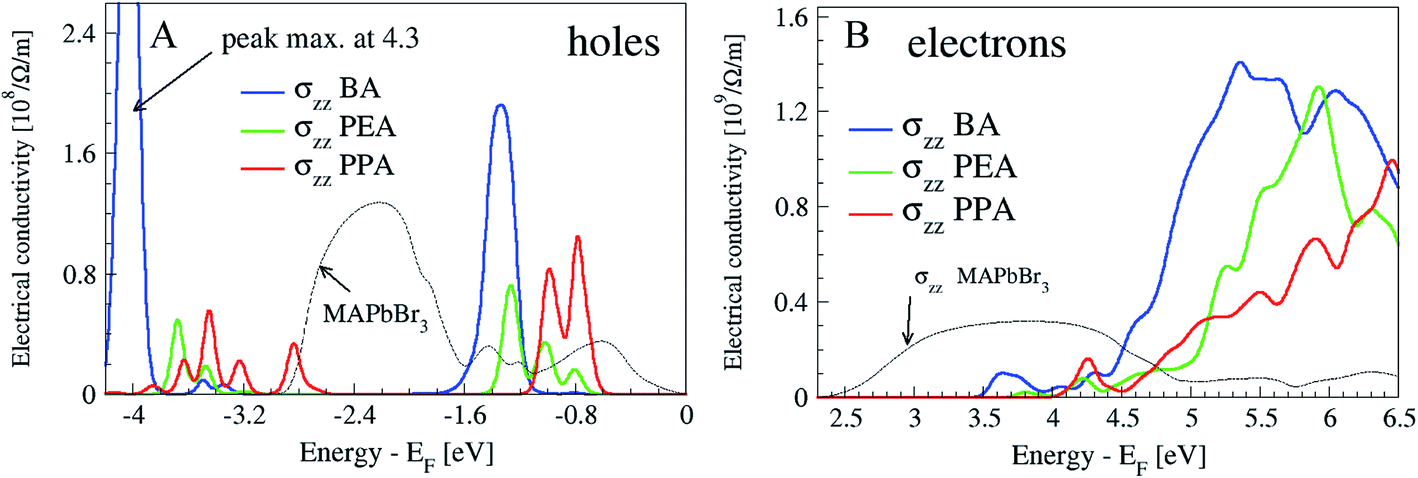 | ||
| Fig. 4 Electrical conductivity at 300 K, plotted for holes (A) and electrons (B), for the direction across the heterostructures. The top of the valence band (Fermi level) is set at energy zero. | ||
Regarding the holes, the positions of the molecular bands are deeper below VBT for BA than for PEA or PPA (Fig. 5S,† left column). This characteristic works in opposition to the hole-transport when the R value is short, if one thinks in terms of the activation energy needed for creating the hole, which is 1.5 eV for BA and 0.8 for PPA (Fig. 5SB,† left column).
The differential charge density maps of holes and electrons shed more light on the details of the hole delocalization at the interface of the perovskite with the barrier molecules (Fig. 6S†). With BA, holes are delocalized over the whole molecule, whereas for PEA and PPA, they are present more at the phenyl ring. This influences the hole's conductivity strength, which is again highest for BA in comparison with the other barriers (see the maximum of the peak for holes, which is located at −1.5 eV in Fig. 4). The differential charge density maps also support the electronic conductivity picture. The electrons are delocalized over the whole BA molecule, whereas for PEA and PPA the electrons are localized along the R group. Therefore, the highest photovoltaic efficiency for BA (Tables 1 and 2) agrees well with the highest carrier conductivities of BA, as shown in Fig. 4. It is interesting to note that for both electrons and holes the charge density is more localized for PEA (electrons from the R-group and holes at the phenyl ring) than for PPA, which correlates with the higher efficiency and higher Voc value of PEA compared with PPA. It can be concluded that when the charges are localized on the barrier molecule, a better Voc can be achieved, while when the charges are delocalized better current density can be achieved.
| R | V oc (V) | J sc (mA cm−2) | FF (%) | Efficiency (%) |
|---|---|---|---|---|
| No barrier | 1.23 ± 0.05 (1.32) | 9.5 ± 0.8 (10.0) | 62 ± 5 (67) | 7.2 ± 1.2 (8.9) |
| BA | 1.35 ± 0.03 (1.31) | 10.1 ± 0.6 (11.5) | 65 ± 2 (63) | 8.8 ± 0.4 (9.5) |
| PEA | 1.45 ± 0.03 (1.45) | 9.0 ± 0.3 (9.0) | 59 ± 4 (65) | 7.5 ± 0.6 (8.6) |
| PPA | 1.25 ± 0.02 (1.24) | 8.5 ± 0.5 (9.5) | 59 ± 3 (60) | 6.3 ± 0.4 (7.1) |
In addition to PSCs without the HTM, we studied the quasi 2D perovskite cells with different barriers using spiro as the HTM. Table 2 summarizes the average and the best PV results. Here, BA showed the best PV performance, achieving 9.5% efficiency and 11.5 mA cm−2 current density which approach the Shockley and Queisser limit. The trend regarding the PV performance is the same as for HTM-free cells. The corresponding JV curves and the EQE spectra of the cells with spiro as the HTM are shown in Fig. 5B and 8SA.† The shape of the EQE spectra is in good agreement with the absorbance response of the bromide quasi 2D perovskite for n = 50. JV curves at different scan rates were measured for the quasi 2D and the 3D PSCs. No difference was observed in the JV curves for various scan rates (Fig. 8SB†), which supports the stability of the PV measurements.
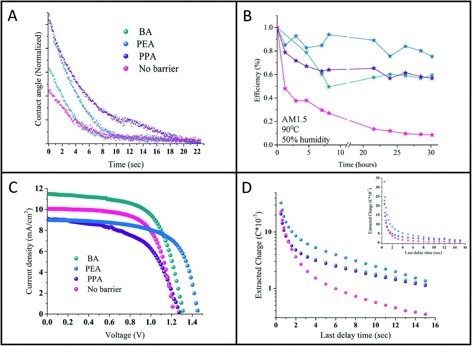 | ||
| Fig. 5 (A) The change in the contact angle of a drop of triple distilled water (TDW) on the studied perovskites' surfaces deposited on the TiO2 substrate. (B) Stability measurements of the cells using the different barrier molecules under 1 sun illumination, 90 °C and 50% humidity. (C) J–V curves of the best-performing cells observed for the quasi-2D (n = 50) and 3D perovskites with the use of spiro as a hole transport layer. (D) Charge extraction measurements for the different barriers and the 3D perovskite. | ||
Contact angle measurements were performed on the studied perovskites' surface. It was assumed that the long hydrophobic organic chain of the barrier will provide moisture resistance to the perovskite. Previous studies on the stability of perovskites with low n values showed an enhancement in resistance to humidity.10–12 Here, contact angle measurements were conducted on the n = 50 samples for the various barriers. The change in the contact angle with time of a triple distilled water (TDW) drop on the perovskite surface was measured. Fig. 5C shows the change in the contact angle with time. The images of the initial drop and the drop at the final stage can be observed in Fig. 9S.† As shown, the initial angle is different for the various barriers, where for 3D = 56.7°, BA = 57.9°, PEA = 69.1°, and PPA = 69.7°. As the angle widens, the nature of the perovskite surface becomes more hydrophobic. In addition, as shown in Fig. 5C, PPA required the longest time to reach a low contact angle, whereas the 3D perovskite required the shortest time. It can be concluded that PPA has the most hydrophobic nature, followed by PEA, BA, and the 3D perovskite. The better hydrophobic nature indicates the better stability of the quasi 2D perovskite in ambient air, even at high n values such as n = 50.
The PV performance of the cells was tracked for 60 days, where the cells were stored in a nitrogen environment between measurements. The cells' PV performance didn't decrease during that time (see Fig. 11S†). In addition, stability measurements under harsh conditions of 1 sun illumination, 90 °C and 50% humidity were applied. The quasi 2D cells show enhanced stability compared to the 3D cells (see Fig. 5B). It can be observed that the 3D cells degredate after 1 hour to half of their initial efficiency, where since then their efficiency decreased to zero after 20 hours. On the other hand, the efficiency of the quasi 2D cells decreased slowly to 60% of their initial efficiency and stayed constant at this value.
The hysteresis curves of the quasi 2D perovskite with the different barriers and the 3D perovskite are presented in Fig. 7S.† The hysteresis is largest for the longest R-group (i.e., PPA) case and smallest for the small barrier (i.e., BA) and the 3D perovskite. This is well supported by the differential charge density maps: both holes and electrons are delocalized for BA, as well as for pure MAPbBr3. In addition, as discussed before, the distances between the perovskite layers (Br–Br) increase with the R group; therefore, charges are more prohibited with the PPA and PEA barriers than with BA and the 3D perovskite, which results in enhanced hysteresis for PPA and PEA.
Charge extraction measurements were performed on the quasi 2D perovskite cells with the different barriers and on the 3D perovskite cell. The charge extraction method includes several steps, as we previously described.15Fig. 5D shows the charge extracted plot vs. the delay time for the different cells. The difference between the 3D perovskite-based cell and the quasi 2D perovskite-based cells is clearly observed. With the quasi 2D-based cells, more charges are left to be extracted compared with the 3D cell. In addition, there is a slight difference between the PEA and the BA and PPA cells; however, for longer delay times, this difference diminishes. As was previously reported,15 in the case of high n values (i.e. the quasi 2D perovskite), more charges are accumulated at the interface barrier/perovskite compared to low n values. Therefore, more charges are left to be extracted with the quasi 2D perovskite compared with the 3D perovskite. Moreover, as stated above, based on the charge density maps, electrons and holes are localized for the PEA case than for PPA and BA, which might also explain the slight difference in the short delay time between the barriers.
Conclusions
This paper investigated the optical and physical properties of bromide quasi 2D perovskites synthesized using different barrier molecules. The various bromide quasi 2D perovskites were introduced into two PV cell configurations with and without HTM. The use of the quasi 2D perovskite as an absorbing layer in PSCs yields improved efficiencies and open circuit voltage as compared to 3D PSCs. Different barriers in the quasi 2D structures have been proved to affect the photovoltaic performance; the cells' performance gets reduced with increasing barrier length. However, the perovskite's hydrophilic character is suppressed with an increase in the chain length of the barrier molecule. A high open circuit voltage of 1.37 V and close to 8% efficiency were observed for full bromide quasi 2D perovskite cells without the HTM with BA as the barrier, and an efficiency of 9.5% (one of the highest values reported) was observed for the same barrier with the HTM. All three barriers exhibited better PV performance and open circuit voltage than the 3D perovskite. It was found that the energy gap and the exciton binding energy extracted using the Elliot formula do not change as a result of the barrier molecule. DFT and spin–orbit coupling calculations showed the decrease in electrical conductivity when the length of the barrier molecule is increased. Moreover, it was shown that when the charges are localized on the barrier molecule, better Voc is achieved, whereas when the charges are delocalized, better current density can be achieved. Finally, contact angle and stability measurements under extreme conditions were performed. The quasi 2D perovskite showed better stability than the 3D perovskite. The contact angle measurements clearly showed the hydrophobic nature of the quasi 2D perovskite compared with the 3D perovskite.Experimental
Perovskite precursor synthesis and solution preparation
Methylammonium bromide (MABr) was synthesized by reacting 29 mL of methylamine (40% in methanol, TCI) with 100 mL of hydrobromic acid (48 wt% in water, Aldrich) in a 250 mL round bottom flask at 0 °C for 2 hours with stirring. The solvent was removed in a rotary evaporator at 50 °C for 1 hour and the precipitate was collected. The precipitate was filtered and washed with diethyl ether repeatedly three times, and the white solid was collected and dried at 60 °C in a vacuum oven for 24 h.Benzyl ammonium bromide (BABr)/phenylethyl ammonium bromide (PEABr)/propylphenylammonium bromide (PPABr) was synthesized by dropwise addition of hydrobromic acid (48 wt% in water, Aldrich) in excess to a stirred solution of 10 mL of phenylethyl ammonium dissolved in 10 mL of absolute ethanol at 0 °C. After the addition of the acid, the precipitate was left for 20 minutes at the same temperature. The precipitate was then washed repeatedly three times with diethyl ether and recrystallized twice with absolute ethanol.
The perovskite solutions were prepared by dissolving stoichiometric quantities of components according to the molecular formula (R)2(MA)n−1PbnBr3n+1 in a 1![[thin space (1/6-em)]](https://www.rsc.org/images/entities/char_2009.gif) :1 ratio of γ-butyrolactone (GBL):dimethyl sulfoxide (DMSO), at 2 M concentration.
:1 ratio of γ-butyrolactone (GBL):dimethyl sulfoxide (DMSO), at 2 M concentration.
Device fabrication
The TiO2 nanoparticles (20 nm, dyesol) were diluted in a 1:4 ratio in ethanol and spin-coated (5000 rpm, 30 seconds) onto a substrate with the architecture of SnO2:F(FTO) conductive glass (15 O cm1, Pilkington) coated by a layer of compact TiO2 (TiDIP, 75% in isopropanol, Aldrich). The substrate was then treated with TiCl4. Perovskite solutions were dropped onto the substrate and spin coated at 1000 rpm for 10 seconds followed by an additional spin of 5000 rpm for 60 seconds; during the second spin 40 μL of toluene was added dropwise onto the substrate. The films were annealed at 100 °C for 1 hour.
For the HTM-fabricated cells, 40 μL of 0.06 M 2,2′,7,7′-tetrakis-(N,N-di-4-methoxyphenyl amino)-9,9′-spirofluorine (spiro-OMeTAD) in chlorobenzene with additives of 26.2 μL/1 mL bis(trifluoromethane)sulfonimide lithium salt in acetonitrile (520 mg mL−1), 29.0 μL/1 mL tris(2-(1H-pyrazol-1-yl)-4-tert-butylpyridine)-cobalt(III) tris(bis(trifluoromethylsulfonyl)imide) in acetonitrile (300 mg mL−1), and 19.2 μL/1 mL of 4-tert-butylpyridine (Aldrich) was spin coated at 4000 rpm for 30 s.
Then, a 70 nm-thick gold electrode was thermally evaporated on the film under a vacuum of ∼10−7 Torr.
400 (Jsc/λϕ), where l is the wavelength, Jsc is the short-circuit photocurrent density (mA cm2), and ϕ is the incident radiative flux (mW cm2). Photovoltaic performance was measured by using a metal mask with an aperture area of 0.04 cm2.
Conflicts of interest
There are no conflicts to declare.Acknowledgements
We wish to thank Israel Chemicals Ltd. Innovation for financial support of this work as well as the Singapore National Research Foundation under the CREATE program: Nanomaterials for Energy and Energy-Water nexus. B.-E. C acknowledges the Israel Ministry of Infrastructure, Energy, and Water under the program for fellowships for PhD students. Calculations were performed in the Cyfronet Computer Centre using the Prometheus computer, which is a part of the PL-Grid Infrastructure. This work was supported by the National Science Centre of Poland (Project No. 2013/11/B/ST3/04041).References
- V. M. Goldschmidt, Naturwissenschaften, 1926, 14, 477–485 CrossRef CAS.
- Z. Li, M. Yang, J.-S. Park, S.-H. Wei, J. J. Berry and K. Zhu, Stabilizing Perovskite Structures by Tuning Tolerance Factor: Formation of Formamidinium and Cesium Lead Iodide Solid-State Alloys, Chem. Mater., 2016, 28, 284–292 CrossRef CAS.
- J. Calabrese, N. L. Jones, R. L. Harlow, N. Herron, D. L. Thorn and Y. Wang, Preparation and Characterization of Layered Lead Halide Compounds, J. Am. Chem. Soc., 1991, 113, 2328–2330 CrossRef CAS.
- S. D. Stranks, G. E. Eperon, G. Grancini, C. Menelaou, M. Alcocer, T. Leijtens, L. M. Herz, A. Petrozza and H. J. Snaith, Electron-Hole Diffusion Lengths Exceeding 1 Micrometer in an Organometal Trihalide Perovskite Absorber, Science, 2013, 342, 341–344 CrossRef CAS PubMed.
- G. Xing, N. Mathews, S. Sun, S. S. Lim, Y. M. Lam, M. Gratzel, S. Mhaisalkar and T. C. Sum, Long-Range Balanced Electron- and Hole-Transport Lengths in Organic-Inorganic CH3NH3PbI3, Science, 2013, 342, 344–347 CrossRef CAS PubMed.
- Q. Dong, Y. Fang, Y. Shao, P. Mulligan, J. Qiu, L. Cao and J. Huang, Electron-Hole Diffusion Lengths > 175 Mu M in SolutionGrown CH3NH3PbI3 Single Crystals, Science, 2015, 347, 967–970 CrossRef CAS PubMed.
- A. Miyata, A. Mitioglu, P. Plochocka, O. Portugall, J. Tse-Wei Wang, S. D. Stranks, H. J. Snaith and R. J. Nicholas, Direct measurement of the exciton binding energy and effective masses for charge carriers in organic–inorganic tri-halide perovskites, Nat. Phys., 2015, 11, 582–587 CrossRef CAS.
- E. A. Muljarov, S. G. Tikhodeev, N. A. Gippius and T. Ishihara, Excitons in self-organized semiconductor/insulator superlattices: PbI-based perovskite compounds, Phys. Rev. B: Condens. Matter Mater. Phys., 1995, 51, 14370–14378 CrossRef CAS.
- T. Ishihara, J. Lumin., 1994, 60–61, 269–274 CrossRef CAS.
- I. C. Smith, E. T. Hoke, D. Solis-Ibarra, M. D. McGehee and H. I. Karunadasa, A Layered Hybrid Perovskite Solar-Cell Absorber with Enhanced Moisture Stability, Angew. Chem., Int. Ed., 2014, 53, 11232–11235 CrossRef CAS PubMed.
- L. N. Quan, M. Yuan, R. Comin, O. Voznyy, E. M. Beauregard, S. Hoogland, A. Buin, A. R. Kirmani, K. I. Zhao, A. Amassian, D. Ha Kim and E. H. Sargent, Ligand-Stabilized Reduced-Dimensionality Perovskites, J. Am. Chem. Soc., 2016, 138(8), 2649–2655 CrossRef CAS PubMed.
- C. C. Stoumpos, D. H. Cao, D. J. Clark, J. Young, J. M. Rondinelli, J. I. Jang, J. T. Hupp and M. G. Kanatzidis, Ruddlesden−Popper Hybrid Lead Iodide Perovskite 2D Homologous Semiconductors, Chem. Mater., 2016, 28, 2852–2867 CrossRef CAS.
- D. H. Cao, C. C. Stoumpos, O. K. Farha, J. T. Hupp and M. G. Kanatzidis, 2D Homologous Perovskites as Light-Absorbing Materials for Solar Cell Applications, J. Am. Chem. Soc., 2015, 137, 7843–7850 CrossRef CAS PubMed.
- H. Tsai, W. Nie, J.-C. Blancon, C. C. Stoumpos, R. Asadpour, B. Harutyunyan, A. J. Neukirch, R. Verduzco, J. J. Crochet, S. Tretiak, L. Pedesseau, J. Even, M. A. Alam, G. Gupta, J. Lou, P. M. Ajayan, M. J. Bedzyk, M. G. Kanatzidis and A. D. Mohite, High-efficiency two-dimensional Ruddlesden–Popper perovskite solar cells, Nature, 2016, 536, 312–317 CrossRef CAS PubMed.
- B. E. Cohen, M. Wierzbowska and L. Etgar, High Efficiency and High Open Circuit Voltage in Quasi 2D Perovskite Based Solar Cells, Adv. Funct. Mater., 2017, 1604733 CrossRef.
- B. Cai, Y. Xing, Z. Yang, W.-H. Zhang and J. Qiu, High performance hybrid solar cells sensitized by organolead halide perovskites, Energy Environ. Sci., 2013, 6, 1480 CAS.
- E. Edri, S. Kirmayer, D. Cahen and G. Hodes, High Open-Circuit Voltage Solar Cells Based on Organic–Inorganic Lead Bromide Perovskite, J. Phys. Chem. Lett., 2013, 4, 897–902 CrossRef CAS PubMed.
- N. Arora, S. Orlandi, M. Ibrahim Dar, S. Aghazada, G. Jacopin, M. Cavazzini, E. Mosconi, P. Gratia, F. De Angelis, G. Pozzi, M. Graetzel and M. K. Nazeeruddin, ACS Energy Lett., 2016, 1, 107–112 CrossRef CAS.
- J. H. Heo, D. H. Song and S. HyukIm, Planar CH3NH3PbBr3 hybrid solar cells with 10.4% power conversion efficiency, fabricated by controlled crystallization in the spin-coating process, Adv. Mater., 2014, 26, 8179–8183 CrossRef CAS PubMed.
- B.-E. Cohen, S. Aharon, A. Dymshits and L. Etgar, Impact of Anti-Solvent Treatment on Carrier Density in Efficient Hole Conductor Free Perovskite based Solar Cells, J. Phys. Chem. C, 2016, 120(1), 142–147 CAS.
- J. Shi, H. Wei, S. Lv, X. Xu, H. Wu, Y. Luo, D. Li and Q. Meng, Control of Charge Transport in the Perovskite CH 3NH 3PbI 3 Thin Film, ChemPhysChem, 2015, 16, 842–847 CrossRef CAS PubMed.
- K. Liang, D. B. Mitzi and M. T. Prikas, Synthesis and Characterization of Organic-Inorganic Perovskite Thin Films Prepared Using a Versatile Two-Step Dipping Technique, Chem. Mater., 1998, 10, 403–411 CrossRef CAS.
- B. Saparov and D. B. Mitzi, Organic–Inorganic Perovskites: Structural Versatility for Functional Materials Design, Chem. Rev., 2016, 116, 4558–4596 CrossRef CAS PubMed.
- X. Hong, T. Ishihara and A. V. Nurmikko, Phys. Rev. B: Condens. Matter Mater. Phys., 1992, 45, 6961 CrossRef CAS.
- T. Ishihara, X. Hong, J. Ding and A. V. Nurmikko, Dielectric confinement effect for exciton and biexciton states in Pbla-based two-dimensional semiconductor structures, Surf. Sci., 1992, 267, 323–326 CrossRef CAS.
- L. V. Keldysh, Coulomb Interaction in Thin Semiconductorand Semimetal Films, JETP Lett., 1979, 29, 658–661 Search PubMed.
- E. Hanamura, N. Nagaosa, M. Kumagai and T. Takagahara, Quantum Wells with Enhanced Exciton Effects and Optical Nonlinearity, Mater. Sci. Eng., B, 1988, 1, 255–258 CrossRef.
- K. Tanaka, T. Takahashi, T. Kondo, T. Umebayashi, K. Asai and K. Ema, Image Charge Effect on Two-Dimensional Excitons in an Inorganic-Organic Quantum-well Crystal, Phys. Rev. B: Condens. Matter Mater. Phys., 2005, 71, 045312 CrossRef.
- W.-J. Yin, T. Shi and Y. Yan, Unusual defect physics in CH3NH3PbI3 perovskite solar cell absorber, Appl. Phys. Lett., 2014, 104, 063903 CrossRef.
- J. L. Knutson, J. D. Martiand and D. B. Mitzi, Tuning the Band Gap in Hybrid Tin Iodide Perovskite Semiconductors Using Structural Templating, Inorg. Chem., 2005, 44(13), 4699–4707 CrossRef CAS PubMed.
- J. H. Heo, D. H. Song and S. HyukIm, Adv. Mater., 2014, 26, 8179 CrossRef CAS PubMed.
- N. Sestu, M. Cadelano, V. Sarritzu, F. Chen, D. Marongiu, R. Piras, M. Mainas, F. Quochi, M. Saba, A. Mura and G. Bongiovanni, Absorption F-Sum Rule for the Exciton Binding Energy in Methylammonium Lead Halide Perovskites, J. Phys. Chem. Lett., 2015, 6, 4566–4572 CrossRef CAS PubMed.
- R. Elliott, Intensity of Optical Absorption by Excitons, Phys. Rev., 1957, 108, 1384–1389 CrossRef CAS.
- D. B. Mitzi, et al., conducting tin halides with a layered organic- based perovskite structure, Nature, 1994, 369, 467–469 CrossRef CAS.
- Y. Takeoka, K. Asai, M. Rikukawa and K. Sanui, Systematic Studies on Chain Lengths, Halide Species, and Well Thicknesses for Lead Halide Layered Perovskite Thin Films, Bull. Chem. Soc. Jpn., 2006, 79(10), 1607–1613 CrossRef CAS.
- L. Etgar, P. Gao, Z. Xue, Q. Peng, A. K. Chandiran, B. Liu, M. K. Nazeeruddin and M. Grätzel, Mesoscopic CH3NH3PbI3/TiO2 Heterojunction Solar Cells, J. Am. Chem. Soc., 2012, 134(42), 17396–17399 CrossRef CAS PubMed.
Footnote |
| † Electronic supplementary information (ESI) available. See DOI: 10.1039/c7se00311k |
| This journal is © The Royal Society of Chemistry 2017 |