
Interface modification effects using a halide-free lead source for perovskite solar cells†
Li
Xiao
a,
Jia
Xu
ab,
Jing
Chen
a,
Jicheng
Luan
a,
Yi
Yang
a,
Bing
Zhang
ab,
Jianxi
Yao
 *ab and
Songyuan
Dai
*ab
*ab and
Songyuan
Dai
*ab
aBeijing Key Laboratory of Novel Thin Film Solar Cells, Renewable Energy School, North China Electric Power University, Beijing 102206, China. E-mail: jianxiyao@ncepu.edu.cn; sydai@ncepu.edu.cn
bBeijing Key Laboratory of Energy Security and Clean Utilization, Renewable Energy School, North China Electric Power University, Beijing 102206, China
First published on 22nd May 2017
Abstract
The remnant PbI2 at the mesoporous-TiO2 (m-TiO2)/CH3NH3PbI3 interface can act as an interface modification layer for high-efficiency perovskite solar cells (PSCs). In this study, we adopted Pb(CH3COO)2·3H2O (PbAc2) to control the amount of remnant PbI2 at the m-TiO2/CH3NH3PbI3 interface. The characterization results demonstrate that the amount of remnant PbI2 could be controlled by the concentration of PbAc2 solution without influencing the crystallographic textures of CH3NH3PbI3 films. By adjusting the PbAc2 solution concentration, the optimized PSC can achieve a 15% enhancement of PCE in the case of using a two-step method for CH3NH3PbI3 preparation. Under the circumstances of using an anti-solution method, it still displayed a 10% enhancement of the average PCE for 10 individual PSCs with PbAc2 (13.6% to 15.0%). The steady-state photoluminescence (PL), time-resolved photoluminescence (TR-PL) and open-circuit voltage decay results demonstrated that the remnant PbI2 could reduce carrier recombination at the m-TiO2/CH3NH3PbI3 interface. Meanwhile, the enhancement of the open-circuit voltage was achieved for PSCs with PbAc2.
Introduction
Organic–inorganic lead halide perovskites have attracted tremendous attention as excellent materials for photovoltaic applications.1,2 These materials exhibit good absorption coefficients,3 tunable band gaps,4 long electron–hole diffusion lengths and high carrier mobility.5–7 Recently, perovskite solar cells (PSCs) have been of primary interest because of their super performance and power conversion efficiency (PCE) of 22.1%.8 Guaranteeing the effective separation of most photo-generated carriers before recombination occurs in PSCs remains one of the key factors.9,10 In this regard, to improve device performance, it is essential to reduce the carrier recombination.11–13Interface modification at the TiO2/perovskite interface and solvent engineering aiming to improve perovskite quality are major approaches to settle the carrier recombination issue by an improved carrier extraction rate.14–16 An appropriate amount of PbI2 species in the CH3NH3PbI3 film is reported to have a positive effect in improving the photovoltaic performance of PSCs.17 It has been demonstrated that the PbI2 could passivate the surface defects and reduce charge recombination effectively.18 Through a one-step solution process, Anders Hagfeldt et al. obtained PSCs with the efficiency of 20.8% by guaranteeing an excess of PbI2 in the solution for perovskite fabrication.19 In spite of the method for perovskite film preparation, retaining the excess PbI2 is an effective strategy to achieve good performance in PSCs by the vapor and solution process.17,19–21 The Yang Yang group indicated that the conduction band minimum (CBM) and valence band maximum (VBM) for CH3NH3PbI3 are noted to be 3.93 eV and 5.43 eV, respectively, while the CBM and VBM for PbI2 are 3.45 eV and 5.75 eV, respectively.17 This type of band alignment between PbI2 and CH3NH3PbI3 allows for the formation of energy barriers, which could prevent excitons from recombining through non-radiative channels at trap states and surface defects at the interface.17,22 However, a low amount of the remnant PbI2 might not play an important role in avoiding the recombination of carriers. On the other hand, the remnant PbI2 might retard the transfer of not only holes but also electrons under the conditions of a higher amount of PbI2.20 Therefore, it is necessary to perform a systematic investigation about the influence of the amount of remnant PbI2 at the TiO2/CH3NH3PbI3 interface on the performance of PSCs.
In most previous studies, PbI2 was generally used as the lead source.23 Snaith et al. changed lead halide (PbCl2 and PbI2) to a non-halide lead source, PbAc2, via a simple one-step solution-coating technique.24 Their results demonstrated that PbAc2 could accelerate the CH3NH3PbI3 crystal growth. The facile removal of CH3NH3Ac could enhance both the smoothness and surface coverage of the perovskite films. Henk J. Bolink noted that smooth and pinhole-free perovskite layers over a large area could be obtained with a lead acetate precursor.25 It has been proven that PbAc2 and CH3NH3I react to produce PbI42− in the first step, subsequently producing PbI2. Ammonium acetate is significantly easier to volatilize, and can avoid the additional introduction of a halogen element.26,27 In these research studies, the remnant of PbI2 is controlled by employing higher PbI2 concentration or the decomposition of CH3NH3PbI3. Actually, the amount of the remnant PbI2 is hard to regulate and an excess of the halogen element might be introduced into the reaction system.
In this study, PbAc2 is used to control the amount of remnant PbI2, and furthermore improve the performance of PSCs. The results demonstrate that adjusting the concentration of PbAc2 solution is an effective approach for controlling the amount of remnant PbI2 at the TiO2/CH3NH3PbI3 interface. The adoption of PbAc2 could avoid the uncertainty amount of remnant PbI2 by higher PbI2 concentration or decomposition of CH3NH3PbI3. When PbAc2 is used to adjust the PbI2 amount at the m-TiO2/perovskite interface, smoother and more uniform CH3NH3PbI3 films are obtained within a two-step method. Upon changing the concentration of the PbAc2 solution, the amount of remnant PbI2 could be easily adjusted. The interface modification effect of remnant PbI2 on the PSCs is investigated using steady-state PL and TR-PL. The optimized PSC exhibits a PCE of 11.7%, a 15% enhancement compared to that of the PSC without PbAc2. Subsequently, by an anti-solvent method, an increase of the average PCE of PSCs of 10% (from 13.6% to 15.0%) with a 70 mV enhancement on Voc is observed. By understanding and utilizing the generation of remnant PbI2 ascribed to the introduction of PbAc2, it is believed that the synthesis technique provides an effective and efficient approach to improve the properties of the interface and increase the performance of PSCs.
Experimental section
Materials
The TiO2 paste with 18 nm particles (Dyesol) was diluted with ethanol with a 1![[thin space (1/6-em)]](https://www.rsc.org/images/entities/char_2009.gif) :3.5 weight ratio. Lead acetate (PbAc2, 98%) was purchased from Aladdin. CH3NH3I and spiro-OMeTAD(2,2′,7,7′-tetrakis(N,N-di-p-methoxyphenylamine)-9,9-spirobifluorene) powders were purchased from Ningbo Borun New Material Technology Co., Ltd. PbI2 (99%) was purchased from Acros. The N,N-dimethyl formamide (DMF), dimethyl sulfoxide (DMSO) and chlorobenzene solvents were purchased from Alfa Aesar. Isopropanol was obtained from J&K Chemicals. FK209 (tris(2-(1H-pyrazol-1-yl)-4-tert-butylpyridine)cobalt(III)) bis(trifluoromethylsulfonyl)imide was purchased from Shanghai MaterWin New Materials Co., Ltd, and lithium bis(trifluoromethanesulfonyl)imide (Li-TFSI) (99.95%) was purchased from Aldrich.
:3.5 weight ratio. Lead acetate (PbAc2, 98%) was purchased from Aladdin. CH3NH3I and spiro-OMeTAD(2,2′,7,7′-tetrakis(N,N-di-p-methoxyphenylamine)-9,9-spirobifluorene) powders were purchased from Ningbo Borun New Material Technology Co., Ltd. PbI2 (99%) was purchased from Acros. The N,N-dimethyl formamide (DMF), dimethyl sulfoxide (DMSO) and chlorobenzene solvents were purchased from Alfa Aesar. Isopropanol was obtained from J&K Chemicals. FK209 (tris(2-(1H-pyrazol-1-yl)-4-tert-butylpyridine)cobalt(III)) bis(trifluoromethylsulfonyl)imide was purchased from Shanghai MaterWin New Materials Co., Ltd, and lithium bis(trifluoromethanesulfonyl)imide (Li-TFSI) (99.95%) was purchased from Aldrich.
Device fabrication
Fluorine-doped tin oxide (FTO) glass (15 Ω □−1) was first etched from one side by HCl and Zn powder. The etched substrates were sequentially cleaned in alkaline liquor, soapy water, deionized water, and ethanol in an ultrasonic bath. Then, the substrates were calcined at 500 °C in air. A compact TiO2 (c-TiO2) blocking layer was formed on FTO by spin-coating tetrabutyltitanate (20 mM in isopropanol) at 3000 rpm for 30 s, which was followed by annealing at 500 °C for 30 minutes in air. The diluted TiO2 paste was then spin-coated on top at 5000 rpm for 30 s and calcined at 500 °C for 30 minutes to form a mesoporous-TiO2 (m-TiO2) layer. The FTO/c-TiO2/m-TiO2 anode used in this study was noted as A. Then PbAc2 solution in a mixed solvent of glycerol and DMF (volume ratio, 1:3) was spin-coated. Several PbAc2 concentrations, including without PbAc2 (PA0), 50 mg mL−1 (PA50), 100 mg mL−1 (PA100), and 150 mg mL−1 (PA150), were adopted under a PbI2 layer to prepare PSCs.
The PbI2 solution was dissolved and kept at 70 °C at a concentration of 462 mg mL−1. All A/PbAc2/PbI2 films were heated on a hot stage at 70 °C for 30 min. After cooling to room temperature, CH3NH3I solution (8.5 mg mL−1 in isopropanol) was sprayed on top of the lead layer, and a reaction time of 30 s was guaranteed before spin-coating. The as-prepared CH3NH3PbI3 films were heated at 70 °C for 30 min on a hot plate. For improvement, an anti-solution method was also used to prepare CH3NH3PbI3 films onto A/PbAc2. CH3NH3I and PbI2 (molar ratio, 1:1) of 1.2 M in a mixture of DMSO and DMF (v/v = 8:2) were dissolved at 60 °C. A spin-coating process was set at 1000 rpm and 5000 rpm for 20 s and 30 s, respectively. At the last 10 s of the second spin-coating step, the substrate was treated with chlorobenzene. The substrates were heated at 105 °C for 60 min to complete crystallization of CH3NH3PbI3 films.
Subsequently, 20 μL of a spiro-OMeTAD solution was spin-coated on the perovskite layer at 4000 rpm for 30 s. The solution was prepared by mixing 72.3 mg of spiro-OMeTAD, 28.8 μL of TBP (4-tert-butylpyridine), 17.5 μL of LiTFSI (520 mg mL−1 in acetonitrile) and 29 μL of FK209 (300 mg mL−1 in acetonitrile) in 1 mL of acetonitrile. Finally, the back contact was made by thermally evaporating a 60 nm thick gold film on top of the device. A 3 mm × 3 mm square mask was cleaved on the glass side before photovoltaic performance characterization.
Characterization and measurements
Scanning electron microscopy (SEM) images were taken with a SU8010 (Hitachi, Japan). The measurement was conducted at 5.0 kV, 10 μA. X-ray diffraction was measured by using a D8 FOCUS (Bruker, German) which was equipped with a Cu Kα X-ray (λ = 1.5406 Å) tube. Ultraviolet-visible (UV-Vis) absorbance spectra were measured with a UV2400 (Shimadzu, Japan) from 350 to 800 nm. An AC Mode III (Agilent, America) atomic force microscope (AFM) was used to measure the surface morphology of the thin films in tapping mode. Time-resolved photoluminescence (TR-PL) measurements (F900, UK) of the A/PA/CH3NH3PbI3 samples were obtained by excitation with a 480 nm laser light under ambient air conditions at the Technical Institute of Physics and Chemistry of China. The steady-state PL was measured at the excitation wavelength of 510 nm with a FL4600 (Hitachi, Japan).The photovoltaic performance was measured with a Keithley 2400 sourcemeter under AM 1.5 irradiation generated by a solar simulator (XES 300T1, SAN-EI Electric Co., Japan). The intensity of the irradiation was calibrated by a standard Si reference cell. The incident photo-to-current efficiency (IPCE) was characterized by a QE-R system (Enli Tech.) under ambient conditions. The Voc decay within 1000 μs was recorded using an electrochemical workstation (Zahner ennium, Germany) with PSCs illuminated under LED white light of 1000 W m−2.
Results and discussion
The XRD results of the A/PA/CH3NH3PbI3 samples with different PbAc2 concentrations are shown in Fig. 1. As shown in Fig. 1, seven peaks marked by black pentagrams and located at 14.1°, 20.2°, 24.5°, 28.5°, 32.0°, 40.7° and 43.3° can be observed, corresponding to the (110), (112), (111), (220), (310), (224) and (314) crystal planes of the β-phase CH3NH3PbI3, respectively.28,29 The peaks marked with A are related to the diffraction patterns of FTO/c-TiO2/m-TiO2 anodes, which are in good agreement with previous reports.30,31 The peak marked with an inverted triangle, located at 12.9°, is indexed to the (001) plane of PbI2.32 With the increase of the PbAc2 solution concentrations, the peak intensity of the remnant PbI2 enhanced. The results indicate that the amount of remnant PbI2 could be adjusted through controlling PbAc2 concentration. The reaction process is given in formula (1) according to the XRD results. Such a method is easy to operate and might contribute to modifying the photovoltaic performance of PSCs.| PbAc2 + PbI2 + 3CH3NH3I → PbI2 + CH3NH3PbI3 + 2CH3NH3Ac↑ |
 | ||
| Fig. 1 XRD results of the A/PA/CH3NH3PbI3 samples with different concentrations of PbAc2 involved (from the bottom to the top: PA0–PA150). | ||
The quality of CH3NH3PbI3 films is of vital importance for the performance of PSCs.33,34 The morphologies of the CH3NH3PbI3 films characterized by SEM are shown in Fig. 2. Without the adoption of PbAc2, the CH3NH3PbI3 particles showed a cubic shape with an average size of 300 nm. The CH3NH3PbI3 film could not fully cover the m-TiO2 layer. From Fig. 2(a), it can be seen that some pin-holes are distributed on the surface of the CH3NH3PbI3 film. The pin-holes might cause the recombination of electrons and holes.35,36Fig. 2(b) shows the morphology of CH3NH3PbI3 with the PbAc2 solution concentration of 100 mg mL−1. In contrast, through the adoption of PbAc2 solution, pin-hole free films were obtained and the cubic CH3NH3PbI3 connected each other tightly, it is encouraging that the surface coverage of the perovskite films on m-TiO2 by a two-step solution process is greatly improved with the adoption of PbAc2. The cross-sectional image of the A/PA/CH3NH3PbI3 samples in Fig. 2 displays that the thickness of the CH3NH3PbI3 layer is around 200 nm. As displayed in Fig. 2(c)–(f), all perovskite films infiltrated well into the m-TiO2 films, which is beneficial for the interface connection between the m-TiO2 and perovskite layers.37
 | ||
| Fig. 2 SEM of A/PA/CH3NH3PbI3 films, including the surface morphologies of PA0 (a) and PA100 (b); cross-sections of PA0 (c), PA50 (d), PA100 (e) and PA150 (f). | ||
The absorbance spectra of the A/PA/CH3NH3PbI3 samples are displayed in Fig. 3. Four samples involving different PbAc2 concentrations (PA0, PA50, PA100 and PA150) demonstrate similar absorption edges at around 780 nm. The intensity decrease of the absorbance curves from PA0 to PA150 was caused by the increase of the remnant PbI2 amount.20 Consistent with the XRD results, it supports the point that adopting a higher concentration of PbAc2 within a two-step method can efficiently enhance the amount of remnant PbI2.
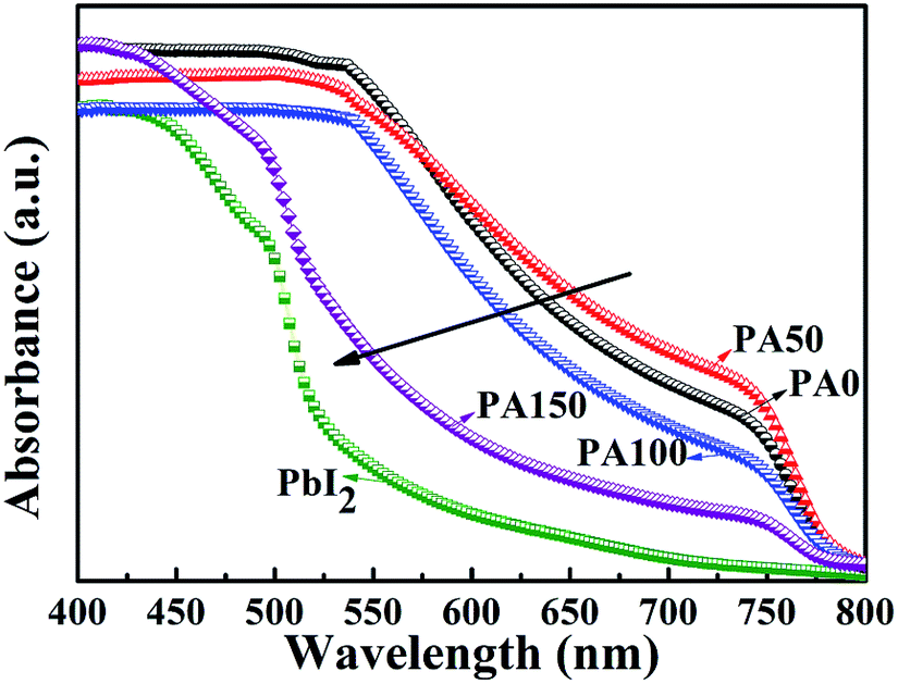 | ||
| Fig. 3 UV-Vis curves of A/PbI2 and A/PA/CH3NH3PbI3 films with different concentrations of PbAc2 involved. | ||
To study the influence of the amount of remnant PbI2 at the m-TiO2/CH3NH3PbI3 interface on the performance of PSCs, the as-prepared perovskite films were used to fabricate the FTO/c-TiO2/m-TiO2/CH3NH3PbI3/spiro-OMeTAD/Au devices. The J–V results measured under simulated AM 1.5G (100 mW cm−2) were carried out to evaluate the performance of the PSCs (Fig. 4). And the photovoltaic parameters are summarized in Table 1. The PSC without introducing PbAc2 shows a Voc of 0.88 V, a Jsc of 18.3 mA cm−2 and a fill factor of 63%, which give an overall PCE of 10.2%. With the concentration of PbAc2 solution increasing from 50 to 150 mg mL−1, the Voc was slightly increased. The voltage exhibits a linear growth from 0.88 V to 1.02 V as a higher concentration of the PbAc2 was deposited. Optimal cells were obtained when PbAc2 solution with the concentration of 100 mg mL−1 PbAc2 was adopted, yielding a Voc of 0.98 V, a Jsc of 18.5 mA cm−2, a fill factor of 64.6% and an overall PCE of 11.7%. Usually, the carrier recombination easily happens when the electron transfer layer is in direct contact with the hole-transport layer.38 As seen from Fig. 2(b), the improvement in the coverage of the CH3NH3PbI3 film on m-TiO2 can effectively reduce the possibility of the electron–hole recombination.20,39 On the other hand, the higher CBM of PbI2 compared to that of CH3NH3PbI3 could prevent excitons from recombining. However, the excessively thick PbI2 blocking layer might slow the electron transfer to the m-TiO2 layers, which would degrade the performance of PSCs as shown by the J–V results of PA150 samples.
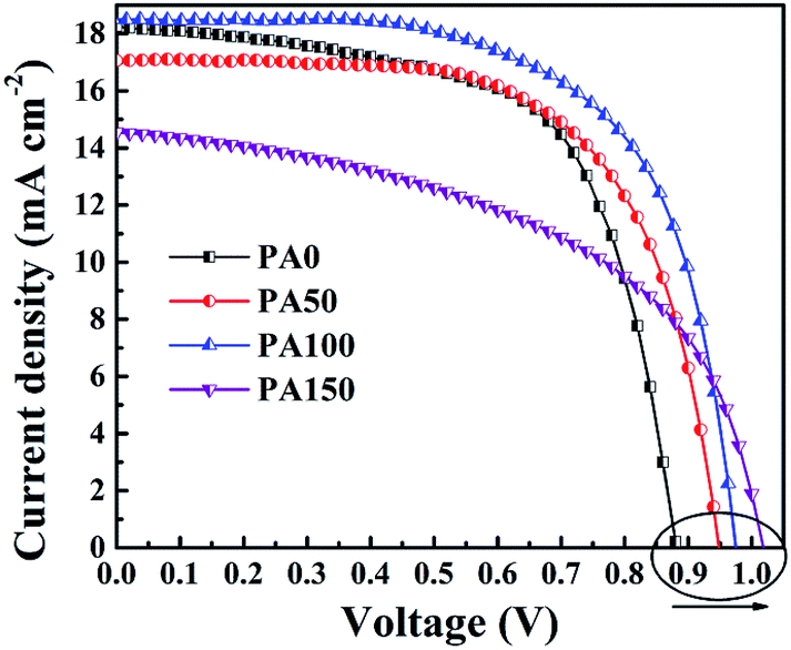 | ||
| Fig. 4 J–V curves of the PSCs with different concentrations of PbAc2 involved. | ||
| Devices | V oc (V) | J sc (mA cm−2) | FF (%) | PCE (%) |
|---|---|---|---|---|
| PA0 | 0.88 | 18.3 | 63.2 | 10.2 |
| PA50 | 0.95 | 17.1 | 64.6 | 10.5 |
| PA100 | 0.98 | 18.5 | 64.6 | 11.7 |
| PA150 | 1.02 | 14.3 | 52.0 | 7.7 |
Time-resolved photoluminescence (TR-PL) measurements were carried out to study the emission lifetime of the A/PA/CH3NH3PbI3 samples of PA0 and PA100 (Fig. 5). All the curves are fitted with three-component exponential decay according to a previous study, the electron lifetime and the calculated percentage can be read from the insert chart. The photoluminescence decay components are attributed to the carrier recombination occurring in the perovskite bulk and surface.40,41 The sample without PbAc2 (PA0) possesses a fast decay of 24.63 ns at a proportion of 62.8%. Compared to PA0, slower photoluminescence decay for samples with 100 mg mL−1 PbAc2 (PA100) is observed. It possesses a fast decay of 36.04 ns at a proportion of 69.2%. As it is reported that the remnant PbI2 would affect the carrier transfer in two ways in PSCs: one is the positive effect that the remnant PbI2 would effectively prevent the holes in the perovskite layer from recombining with the electrons in the m-TiO2; the second is the negative effect that the remnant PbI2 could block the photogenerated electron transfer from the perovskite to the m-TiO2.17 Thus, it is needed to adopt the optimal amount of PbI2 to optimize the performance of PSCs. From the TR-PL results (Fig. 5), it can be seen that the PA100 sample showed a longer electron lifetime than the PA0 case. This result indicates a slower electron extraction rate, which is caused by the block of electron transfer of remnant PbI2. However, a weaker photoluminescence intensity in the steady state PL spectra in Fig. S1† indicates that less electron–hole recombination happens in the sample. As we know, too much amount of the remnant PbI2 at the m-TiO2/perovskite interface would confine electron transfer, which leads to a longer electron lifetime and decreased Jsc in devices. On the other hand, the remnant PbI2 could modify the m-TiO2/perovskite interface, therefore the highest PCE could be obtained in a curtailed PbI2 concentration, which is reported by Bi et al.20 The J–V results in Fig. 4 show similar results, the Jsc tends to decrease when the concentration of PbAc2 solution increases, which is the result of the blocking of electron transfer. However, the Voc gradually increases as the concentration of PbAc2 solution increases, which is the result of the modification effect of the remnant PbI2 at the m-TiO2/perovskite interface. In the case of PA100, the appropriate amount of remnant PbI2 at the m-TiO2/perovskite interface optimizes the performance of PSCs by blocking the electron–hole recombination and interface modification.
 | ||
| Fig. 5 Normalized TR-PL decay curves of the A/PA/CH3NH3PbI3 samples excited by a laser at 485 nm. The data are shown as a scatter plot, and the fittings are in continuous lines. | ||
To explore the reaction of PbAc2 with CH3NH3I (MAI), PbAc2 was individually spin-coated on the top of FTO/c-TiO2/m-TiO2 (A), and the MAI isopropanol solution with a concentration of 10 mg mL−1 is added dropwise on its surface. The XRD diffraction patterns of A, A/PA and A/PA + MAI are shown in Fig. 6. The peaks marked with a black pentagram are assigned to CH3NH3PbI3 for the A/PA + MAI sample. In the absence of the PbI2 layer, there is no clue for remnant PbI2. By further depositing spiro-OMeTAD and the Au electrode, the device displays a PCE of 4.64% with a Jsc of 11.3 mA cm−2 and a Voc of 0.69 V (Fig. S2†). The possible reaction mechanism according to earlier reports is given in the equation below.23,27 To conclude from the above, the Ac− ion is easily replaced by I−, and volatilizes from the film as CH3NH3Ac. In our system, MAI first reacted with PbI2 to form CH3NH3PbI3. After the PbI2 was consumed out, MAI would react with PbAc2, which lead to the formation of new PbI2. Because of the lack of MAI, more CH3NH3PbI3 could not be produced. And then, part of remnant PbI2 from PbAc2 would exist in the films.
| PbAc2 + 3CH3NH3I → CH3NH3PbI3 + 2CH3NH3Ac↑ |
 | ||
| Fig. 6 XRD diffraction patterns of A, A/PA and A/PA + MAI. | ||
Actually, the CH3NH3PbI3 films prepared by the two-step method were not the ideal films in the application of PSCs, and the improvement of CH3NH3PbI3 films is essential for the consideration of PbAc2. An anti-solution method can achieve CH3NH3PbI3 films with good uniformity and surface coverage according to previous studies.42,43 PbAc2 solution of 100 mg mL−1 (PA100) was used for the one-step deposition of CH3NH3PbI3 films. Compared to those of the samples without PbAc2 (PA0), the XRD diffraction patterns of A/PA/CH3NH3PbI3 show an enhancement of remnant PbI2 (Fig. 7(a)). The result is consistent with our previous study which uses the two-step method for the formation of CH3NH3PbI3 films (Fig. 2). As displayed in Fig. S3(a) and (b),† the morphologies of CH3NH3PbI3 films with/without PbAc2 are different, the root mean square roughness of the CH3NH3PbI3 films demonstrates a slight reduction from 30.6 to 26.5 nm by adoption of PbAc2.
 | ||
| Fig. 7 (a) XRD diffraction patterns of A/PA/CH3NH3PbI3 samples in 10–17°, (b) histograms of PCEs measured for 10 individual cells with/without PbAc2, (c) I–V curves and cross-sections of PSCs with/without PA, and (d) IPCE result of PSCs with PA100. | ||
Subsequently, device performances were evaluated after assembling PSCs. Fig. 7(b) and S4(a)† display histograms of PCEs and J–V curves of 10 nominally identical devices with/without PbAc2. Compared to PSCs without PA, a narrow PCE distribution of PSCs with PA100 was achieved (Fig. 7(b)). An average PCE of 15.0% is obtained for PA100 while 13.6% is obtained for PA0. The I–V curves of PSCs with a PCE of 13.4% for PA0 and 15.1% for PA100 are displayed in Fig. 7(c); the Voc is 0.95 V, Jsc is 21.5 mA cm−2, and FF is 65.3% and Voc of 1.03 V, Jsc of 20.8 mA cm−2, FF of 70.2%, respectively (Table 2). The box plots of Voc in Fig. S4(b)† indicate that a statistical increase of Voc of about 70 mV was demonstrated by the adoption of PbAc2. The devices structures with/without PbAc2 are shown in the inset in Fig. 7(c). The IPCE results of PSCs with PA100 in Fig. 7(d) demonstrate good light response within the absorption band (300–800 nm). An integrated Jsc of 20 mA cm−2 was achieved, which is consistent with the J–V results, indicating that most photo-induced electrons are collected and become free carriers.
| Devices | V oc (V) | J sc (mA cm−2) | FF (%) | PCE (%) |
|---|---|---|---|---|
| PA0 | 0.95 | 21.5 | 65.3 | 13.4 |
| PA100 | 1.03 | 20.8 | 70.2 | 15.1 |
Considering the good coverage of CH3NH3PbI3 films on m-TiO2 by the anti-solution method, the increase of the average PCE improvement of 10% could be attributed to the enhancement of remnant PbI2, which can effectively prevent the recombination between the electrons and holes leading to the Voc.7,44 The normalized open-circuit voltage decay curves were acquired as shown in Fig. 8(a). The PSC with PA100 exhibited a longer Voc decay time than the PSC without PbAc2 (PA0). Using the following equation, the electron lifetime τ can be obtained:
| τ = −kBTe−1(dVoc/dt)−1 | (1) |
 | ||
| Fig. 8 (a) Voc decay curves and (b) the relationship between the electron lifetime and the Voc of PSCs with/without PA. | ||
Conclusions
In summary, we have demonstrated that the adoption of PbAc2 is an efficient way to control the amount of remnant PbI2 at the m-TiO2/CH3NH3PbI3 interface. The MAI might first react with PbI2, it is consumed and subsequently reacts with PbAc2. Then, the PbI2 forms due to the incomplete reaction of PbAc2 and MAI. The remnant PbI2 could act as an interface modification layer for PSCs in our study despite the method we use to prepare CH3NH3PbI3 films. However, the introduction of PbAc2 would not influence the crystallinity of the CH3NH3PbI3 films. By adjusting the PbAc2 solution concentration, the optimized PSC can achieve a 15% enhancement of PCE in the case of using a two-step method. Under the circumstances of using an anti-solution method, it still displayed a 10% enhancement of the average PCE for PSCs with PbAc2 (13.6% to 15.0%). The obvious Voc increase of about 70 mV is attributed to the remnant PbI2. Our results suggest that PbAc2 is effective in controlling the amount of remnant PbI2 at the m-TiO2/CH3NH3PbI3 interface, which provides a new way to optimize the performance of PSCs.Acknowledgements
We gratefully acknowledge the financial support from the National High Technology Research and Development Program of China (863 program) under Grant No. 2015AA050602, the National Natural Science Foundation of China (No. 51372083), the Fundamental Research Funds for the Central Universities (No. 2014ZZD07, 2015XS57, 2012ZX14), the Science and Technology Commission of Beijing Municipality, China (No. Z141100003314003), and Jiangsu Province Science and Technology Support Program, China (No. BE2014147-4).References
- K. Liang, D. B. Mitzi and M. T. Prikas, Chem. Mater., 1998, 10, 403–411 CrossRef CAS.
- J. Burschka, N. Pellet, S. J. Moon, R. Humphry-Baker, P. Gao, M. K. Nazeeruddin and M. Grätzel, Nature, 2013, 499, 316–319 CrossRef CAS PubMed.
- M. Shirayama, H. Kadowaki, T. Miyadera, T. Sugita, M. Tamakoshi, M. Kato, T. Fujiseki, D. Murata, S. Hara, T. N. Murakami, S. Fujimoto, M. Chikamatsu and H. Fujiwara, Phys. Rev. Appl., 2016, 5, 014012 CrossRef.
- M. R. Filip, G. E. Eperon, H. J. Snaith and F. Giustino, Nat. Commun., 2014, 5, 5757 CrossRef CAS PubMed.
- Y. Bi, E. M. Hutter, Y. Fang, Q. Dong, J. Huang and T. J. Savenije, J. Phys. Chem. Lett., 2016, 7, 923–928 CrossRef CAS PubMed.
- M. B. Johnston and L. M. Herz, Acc. Chem. Res., 2016, 49, 146–154 CrossRef CAS PubMed.
- W. Ke, D. Zhao, C. R. Grice, A. J. Cimaroli, J. Ge, H. Tao, H. Lei, G. Fang and Y. Yan, J. Mater. Chem. A, 2015, 3, 17971–17976 CAS.
- NREL Best Research-Cell Efficiencies Chart, http://www.nrel.gov/ncpv/images/efficiency_chart.jpg, accessed April 2017.
- J. Shi, X. Xu, D. Li and Q. Meng, Small, 2015, 11, 2472–2486 CrossRef CAS PubMed.
- W. Ke, G. Fang, Q. Liu, L. Xiong, P. Qin, H. Tao, J. Wang, H. Lei, B. Li, J. Wan, G. Yang and Y. Yan, J. Am. Chem. Soc., 2015, 137, 6730–6733 CrossRef CAS PubMed.
- X. Wen, Y. Feng, S. Huang, F. Huang, Y. B. Cheng, M. Greena and A. Ho-Bailliea, J. Mater. Chem. C, 2016, 4, 793–800 RSC.
- X. Li, M. I. Dar, C. Yi, J. Luo, M. Tschumi, S. M. Zakeeruddin, M. K. Nazeeruddin, H. Han and M. Grätzel, Nat. Chem., 2015, 7, 703–711 CrossRef CAS PubMed.
- J. Wang, L. Liu, S. Liu, L. Yang, B. Zhang, S. Feng, J. Yang, X. Meng, W. Fu and H. Yang, Sustainable Energy Fuels, 2017, 1, 504–509 Search PubMed.
- Z. Zhou, J. Xu, L. Xiao, J. Chen, Z. Tan, J. Yao and S. Dai, RSC Adv., 2016, 6, 78585–78594 RSC.
- Y. H. Lee, J. Luo, M. K. Son, P. Gao, K. T. Cho, J. Seo, S. M. Zakeeruddin, M. Grätzel and M. K. Nazeeruddin, Adv. Mater., 2016, 28, 3966–3972 CrossRef CAS PubMed.
- K. Wojciechowski, S. D. Stranks, A. Abate, G. Sadoughi, A. Sadhanala, N. Kopidakis, G. Rumbles, C. Z. Li, R. H. Friend, A. K. Y. Jen and H. J. Snaith, ACS Nano, 2014, 8, 12701–12709 CrossRef CAS PubMed.
- Q. Chen, H. Zhou, T. B. Song, S. Luo, Z. Hong, H. S. Duan, L. Dou, Y. Liu and Y. Yang, Nano Lett., 2014, 14, 4158–4163 CrossRef CAS PubMed.
- S. Wang, W. Dong, X. Fang, Q. Zhang, S. Zhou, Z. Deng, R. Tao, J. Shao, R. Xia, C. Song, L. Hu and J. Zhu, Nanoscale, 2016, 8, 6600–6608 RSC.
- D. Bi, C. Yi, J. Luo, J. D. Décoppet, F. Zhang, S. M. Zakeeruddin, X. Li, A. Hagfeldt and M. Grätzel, Nat. Energy, 2016, 1, 16142 CrossRef CAS.
- D. Bi, A. M. El-Zohry, A. Hagfeldt and G. Boschloo, ACS Photonics, 2015, 2, 589–594 CrossRef CAS.
- D. H. Cao, C. C. Stoumpos, C. D. Malliakas, M. J. Katz, O. K. Farha, J. T. Hupp and M. G. Kanatzidis, APL Mater., 2014, 2, 091101–091107 CrossRef.
- T. Supasai, N. Rujisamphan, K. Ullrich, A. Chemseddine and T. Dittrich, Appl. Phys. Lett., 2013, 108, 183906 CrossRef.
- F. K. Aldibaja, L. Badia, E. Mas-Marzá, R. S. Sánchez, E. M. Barea and I. Mora-Sero, J. Mater. Chem. A, 2015, 3, 9194–9200 CAS.
- W. Zhang, M. Saliba, D. T. Moore, S. K. Pathak, M. T. Hörantner, T. Stergiopoulos, S. D. Stranks, G. E. Eperon, J. A. Alexander-Webber, A. Abate, A. Sadhanala, S. Yao, Y. Chen, R. H. Friend, L. A. Estroff, U. Wiesner and H. J. Snaith, Nat. Commun., 2015, 6, 6142 CrossRef CAS PubMed.
- D. Forgács, M. Sessolo and H. J. Bolink, J. Mater. Chem. A, 2015, 3, 14121–14125 Search PubMed.
- H. Zhu, Y. Fu, F. Meng, X. Wu, Z. Gong, Q. Ding, M. V. Gustafsson, M. T. Trinh, S. Jin and X. Y. Zhu, Nat. Mater., 2015, 14, 636–642 CrossRef CAS PubMed.
- J. Qing, H. T. Chandran, Y. H. Cheng, X. K. Liu, H. W. Li, S. W. Tsang, M. F. Lo and C. S. Lee, ACS Appl. Mater. Interfaces, 2015, 7, 23110–23116 CAS.
- S. Dong, A. Valerio, C. Riccardo, Y. Mingjian, A. Erkki, B. Andrei, C. Yin, H. Sjoerd, R. Alexander, K. Khabiboulakh, L. Yaroslav, Z. Xin, A. D. Peter, F. M. Omar, H. S. Edward and M. B. Osman, Science, 2014, 347, 519–522 Search PubMed.
- H. S. Kim, J. W. Lee, N. Yantara, P. P. Boix, S. A. Kulkarni, S. Mhaisalkar, M. Grätzel and N. G. Park, Nano Lett., 2013, 13, 2412–2417 CrossRef CAS PubMed.
- J. Qiu, Y. Qiu, K. Yan, M. Zhong, C. Mu, H. Yan and S. Yang, Nanoscale, 2013, 5, 3245–3248 RSC.
- Y. Zhao and K. Zhu, J. Phys. Chem. Lett., 2013, 4, 2880–2884 CrossRef CAS.
- N. Li, H. Dong, H. Dong, J. Li, W. Li, G. Niu, X. Guo, Z. Wu and L. Wang, J. Mater. Chem. A, 2014, 2, 14973–14978 CAS.
- S. Ito, S. Tanaka and H. Nishino, J. Phys. Chem. Lett., 2015, 6, 881–886 CrossRef CAS PubMed.
- Y. Zhao and K. Zhu, J. Phys. Chem. Lett., 2014, 5, 4175–4186 CrossRef CAS PubMed.
- Z. Zhu, Y. Bai, T. Zhang, Z. Liu, X. Long, Z. Wei, Z. Wang, L. Zhang, J. Wang, F. Yan and S. Yang, Angew. Chem., 2014, 126, 12779–12783 CrossRef.
- Y. Luo, F. Meng, E. Zhao, Y. Z. Zheng, Y. Zhou and X. Tao, J. Power Sources, 2016, 311, 130–136 CrossRef CAS.
- J. Ye, L. Zhu, L. Zhou, X. Liu, X. Zhang, H. Zheng, G. Liu, Z. Shao, X. Pan and S. Dai, Sol. Energy, 2016, 136, 505–514 CrossRef CAS.
- N. Ahn, D. Y. Son, I. H. Jang, S. M. Kang, M. Choi and N. G. Park, J. Am. Chem. Soc., 2015, 137, 8696–8699 CrossRef CAS PubMed.
- D. Bi, W. Tress, M. I. Dar, P. Gao, J. Luo, C. Renevier, K. Schenk, A. Abate, F. Giordano, J. P. C. Baena, J. D. Decoppet, S. M. Zakeeruddin, M. K. Nazeeruddin, M. Grätzel and A. Hagfeldt, Sci. Adv., 2016, 2, e1501170 Search PubMed.
- M. I. Saidaminov, A. L. Abdelhady, B. Murali, E. Alarousu, V. M. Burlakov, W. Peng, I. Dursun, L. Wang, Y. He, G. Maculan, A. Goriely, T. Wu, O. F. Mohammed and O. M. Bakr, Nat. Commun., 2015, 6, 7586 CrossRef PubMed.
- C. Li, Q. Guo, W. Qiao, Q. Chen, S. Ma, X. Pan, F. Wang, J. Yao, C. Zhang, M. Xiao, S. Dai and Z. Tan, Org. Electron., 2016, 33, 194–200 CrossRef CAS.
- D. Y. Son, J. W. Lee, Y. J. Choi, I. H. Jang, S. Lee, P. J. Yoo, H. Shin, N. Ahn, M. Choi, D. Kim and N. G. Park, Nat. Energy, 2016, 1, 16081 CrossRef CAS.
- N. J. Jeon, J. H. Noh, Y. C. Kim, W. S. Yang, S. Ryu and S. I. Seok, Nat. Mater., 2014, 13, 897–903 CrossRef CAS PubMed.
- X. Sun, Y. Liu, Q. Tai, B. Chen, T. Peng, N. Huang, S. Xu, T. Peng and X. Z. Zhao, J. Phys. Chem. C, 2012, 116, 11859–11866 CAS.
- W. Ke, G. Fang, J. Wan, H. Tao, Q. Liu, L. Xiong, P. Qin, J. Wang, H. Lei, G. Yang, M. Qin, X. Zhao and Y. Yan, Nat. Commun., 2015, 6, 6700 CrossRef CAS PubMed.
Footnote |
| † Electronic supplementary information (ESI) available. See DOI: 10.1039/c7se00200a |
| This journal is © The Royal Society of Chemistry 2017 |