
Construction of efficient photoanodes for dye sensitized solar cells: TiO2 films with a gradient content of graphene
Liguo
Wei
 abc,
Ping
Wang
c,
Yulin
Yang
*c,
Ruiqing
Fan
*c,
Yuze
Yang
a and
Yonglian
Qiu
a
abc,
Ping
Wang
c,
Yulin
Yang
*c,
Ruiqing
Fan
*c,
Yuze
Yang
a and
Yonglian
Qiu
a
aCollege of Environmental and Chemical Engineering, Heilongjiang University of Science and Technology, Harbin 150022, P. R. China
bPrecious Tyrone New Materials Co., LTD, Qitaihe 154603, P. R. China
cMIIT Key Laboratory of Critical Materials Technology for New Energy Conversion and Storage, School of Chemistry and Chemical Engineering, School of Chemical Engineering and Technology, Harbin Institute of Technology, Harbin 150001, P. R. China. E-mail: ylyang@hit.edu.cn; fanruiqing@hit.edu.cn; Fax: +86-451-86418270
First published on 2nd May 2017
Abstract
Graphene has attracted a lot of attention because of its unique optical, thermal, mechanical and electrical properties. In this study, the effect of graphene on the performance of dye sensitized solar cells (DSSCs) was investigated by constructing TiO2 photoanodes with a gradient graphene content. After the construction of photoanodes with a gradient graphene content, the DSSCs displayed a higher dye loading amount, lower internal resistances, lower electron recombination rate and faster electron transport rate, which resulted in high open circuit voltage and current density. Under the optimum conditions, the DSSC exhibited a Voc of 0.72 V, a Jsc of 17.11 mA cm−2, a FF of 0.63, and an energy conversion efficiency (η) of 7.71%, indicating a 41% increase in η than that of the DSSC based on a pure TiO2 photoanode, which gives a Voc of 0.69 V, a Jsc of 12.63 mA cm−2, a FF of 0.62, and an η value of 5.45%. The construction of TiO2 photoanodes with a gradient graphene content could really enhance the efficiency of DSSCs by improving the dye loading amount and enhancing the electron bridge effect of graphene from TiO2 to the FTO, which lowered the electron recombination rate and accelerated the electron transport rate.
1. Introduction
Since the development of dye sensitized solar cells (DSSCs) by the Grätzel group, they have attracted considerable interest owing to their low fabrication costs, simple process and relatively high efficiency.1,2 The performance of DSSCs depends mostly on photoanode materials, since they influence both photovoltage and photocurrent of the solar cells. Nanocrystalline anatase TiO2 has been identified as a promising photoanode material for DSSCs among various photoanode materials and has been widely investigated owing to its superior optical and electrical properties, which play an important role in DSSCs.3–5 However, the photovoltaic performance of DSSCs was still influenced by TiO2 films because the nanocrystalline particles of TiO2 films cannot support an inner electric field and the inner conductivity of TiO2 films is low.6 Although TiO2 nanoparticle photoanodes could adsorb a sufficient number of dye molecules due to their large specific surface area, a trap-limited diffusion process is occurring during electron transport in the TiO2 nanoparticle network.7 A huge number of grain boundaries between nanoparticles are encountered as the generated electrons travel through the nanostructured TiO2 networks inside the photoanode before reaching the collecting electrode, which makes the transport of electrons change to a random walk mode and leads to retardation in electron transport. Also their probability to recombine with electron acceptors in the electrolyte and oxidized dye molecules is increased, thus decreasing the efficiency of DSSCs. Therefore, it is essential to overcome this serious problem with the aim of enhancing the performance of DSSCs. The best way to do this is to design a photoanode with an efficient transport pathway from the photoinjected charge carriers to the current collector.8–10 Several attempts have been made to design such a photoanode to enhance the electron transport and prevent charge recombination, including modifying the morphology of TiO2,11 modifying the surface of TiO2 by doping with nonmetals and metals,12–14 preparing TiO2 bilayer and multilayer structured films,15 coupling TiO2 with another semiconductor, or creating a hybrid with carbonaceous materials such as multi-walled carbon nanotubes (MWCNTs), carbon nanotubes (CNTs), reduced graphene oxide (rGO) and graphene oxide (GO) to direct photogenerated electrons by introducing charge carriers.16–20Graphene is a popular 2D material with unique thermal, mechanical, optical and electrical properties.21–23 It is a zero band gap material with a single molecular layered structure.23 In graphene, each carbon atom uses 3 of its 4 outer orbital electrons to form 3 sigma bonds 120° apart with 3 adjacent carbon atoms in the same plane, leaving the 4th electron free to move; therefore, electrons in graphene behave just like massless relativistic particles without crystal lattice restrictions.24,25 As such, graphene possesses excellent electrical conductivity in two dimensions at room temperature (more than 200![[thin space (1/6-em)]](https://www.rsc.org/images/entities/char_2009.gif) 000 cm2 V−1 s−1).26 Since there are intermolecular forces such as charge transfer interactions, physisorption, or electrostatic binding between graphene and TiO2 nanoparticles,27 TiO2 nanoparticles can anchor on the graphene surface; thus graphene could provide a fast channel for electron transportation,28–31 which lowered the recombination loss and accelerated the electron transport. Therefore, on the basis of the above-mentioned unique properties of graphene, graphene/TiO2 nanocomposites were applied in DSSCs, and were an effective material for retarding electron recombination and accelerating electron transfer in the cell.32–34 However, most groups focus on how to prepare TiO2 composites with graphene and the effect of graphene contents on the performance of DSSCs.35–37 To the best of our knowledge, there is no report on research on the construction of photoanodes with a gradient graphene content.
000 cm2 V−1 s−1).26 Since there are intermolecular forces such as charge transfer interactions, physisorption, or electrostatic binding between graphene and TiO2 nanoparticles,27 TiO2 nanoparticles can anchor on the graphene surface; thus graphene could provide a fast channel for electron transportation,28–31 which lowered the recombination loss and accelerated the electron transport. Therefore, on the basis of the above-mentioned unique properties of graphene, graphene/TiO2 nanocomposites were applied in DSSCs, and were an effective material for retarding electron recombination and accelerating electron transfer in the cell.32–34 However, most groups focus on how to prepare TiO2 composites with graphene and the effect of graphene contents on the performance of DSSCs.35–37 To the best of our knowledge, there is no report on research on the construction of photoanodes with a gradient graphene content.
In this study, the effect of graphene on the performance of dye sensitized solar cells (DSSCs) was further investigated by constructing TiO2 photoanodes with a gradient graphene content. Graphene was prepared by the reduction of graphene oxide (GO) under hydrothermal conditions and graphene/TiO2 composite semiconductor materials with different graphene contents were prepared by mixing graphene into TiO2 paste, and each paste was used to deposit one layer of the photoanode films of dye sensitized solar cells (DSSCs) to construct photoanodes with a gradient graphene content. After the construction of TiO2 photoanodes with a gradient graphene content, the photoanodes displayed a higher dye loading amount, lower internal resistances, faster electron transport rate and lower charge recombination rate, which resulted in the enhanced performance of DSSCs compared with that of cells without graphene. The construction of photoanodes with a gradient graphene content could really enhance the efficiency of DSSCs by improving the dye loading amount and enhancing the electron bridge effect of graphene from TiO2 to the FTO, which accelerated the electron transport rate and lowered the charge recombination rate. The improved performance of DSSCs with the constructed photoanodes is characterized by open-circuit voltage decay, electrochemical impedance spectroscopy and dark current measurement.
2. Materials and methods
2.1 Materials
Commercial TiO2 (P25) nanoparticles were purchased from Degussa Co., Ltd. in Germany. Acetonitrile, I2, LiI, Lithium perchlorate, and tert-butylpyridine were purchased from Tianli Chemical Co., Tianjin, China. An F-doped SnO2-coated glass plate (FTO, 90% transmittance in the visible, 15 Ω cm−2) was purchased from Acros Organics, Belgium, and cleaned by a standard procedure. Di-tetrabutylammonium cis-bis-(isothiocyanato)bis(2,2-bipyridyl-4,4-dicarboxylato)ruthenium(II) (N719) was purchased from Solaronix Company, Switzerland. All other chemical reagents used in the experiments were of analytical reagent grade and purchased from Sinopharm Chemical Reagent Beijing Co., Ltd., without additional purification before use.2.2 Synthesis of graphene
GO was first synthesized according to the method in the literature.35 Then, graphene was prepared following a modified method in the literature. In brief, the as-synthesized GO (0.1 g) was dispersed in water (80 mL) under stirring and was sonicated for 1 h at room temperature. Then the resultant solution was transferred into a Teflon lined stainless steel autoclave, and kept in an oven at 433 K for 48 h. The resulting material was filtered off, washed with ethanol and water, and then dried under vacuum at 323 K for 12 h.2.3 Construction of graphene/TiO2 based photoanodes and DSSC assembly
Before preparing the photoanode films, 100 mg solid state graphene was dissolved in 100 mL ethanol and sonicated for 2 h until a suspended solution of 1 mg mL−1 was formed. Graphene/TiO2 pastes were synthesized following the Grätzel method for preparing TiO2 paste,36 except that 0 mL, 0.25 mL, 0.5 mL, 1.0 mL, 1.5 mL, 2.0 mL, and 2.5 mL graphene solutions were added, respectively. Each paste was printed onto the FTO conductive glass and then dried at 373 K for 5 min. This printing process was repeated with different pastes seven times. The obtained film was then sintered at 773 K for 15 min. It was dyed after being immersed in a solution of 0.3 mM N719 in absolute ethanol for 24 h and then washed with ethanol. By this way, graphene/TiO2 photoanodes with a gradient descent graphene content or with a gradient boost graphene content were prepared. For comparison, the photoanode printed with paste containing 0 mL graphene solution seven times was denoted as Blank, the constructed photoanode printed in sequence with pastes containing 2.5 to 0 mL graphene solutions seven times was denoted as GR-1 and the constructed photoanode printed in sequence with pastes containing 0 to 2.5 mL graphene solution seven times was denoted as GR-2.The solar cell device was sandwich-type and assembled by placing a platinum-coated conductive glass as the counter electrode on the dyed photoanode, and a drop of liquid electrolyte containing 0.5 M LiI, 0.05 M I2, and 0.1 M 4-tert-butylpyridine (TBP) was added to fill the void between the two electrodes which were clipped together as open cells for measurement.
2.4 Characterization
X-ray powder diffraction (XRD) measurement was obtained on a Bruker D8 Advance X-ray diffraction instrument with Cu-Kα radiation. UV-vis spectra were recorded with a UV-2250 spectrophotometer (Shimadzu, Japan). Scanning electron microscopy (SEM) was conducted using a Phenom ProX SEM (Holland). X-ray photoelectron spectroscopy (XPS) was performed with an ESCALAB-250 spectrometer (Thermo, America) with an Al Kα source in an ultrahigh vacuum (UHV) at 3.5 × 10⁻⁷ Pa. The amounts of adsorbed dye were measured by desorbing the dye from the dye-sensitized films in a 0.1 M NaOH solution in water and ethanol (1:1, v/v), and then the concentration of the desorbed dye in the NaOH solution was measured using an UV-visible spectrophotometer. The N2 adsorption–desorption of samples was conducted on a Micromeritics ASAP2020 surface area and pore size analyzer at 196 °C (liquid nitrogen temperature) using accompanying software from Micromeritics. The surface areas were calculated by using the conventional BET method, and the pore size diameters were calculated by using the BJH method. The surface photovoltage spectrum (SPS) was measured on an instrument assembled by Jilin University, in which monochromatic light was obtained by passing light from a 500 W xenon lamp through a double-prism monochromator (SBP300, China), and the signal was collected by a lock-in amplifier (SR830, Stanford). The Raman spectra were determined on a Renishaw inVia micro-Raman spectroscopy system, using the TE air-cooled 576 × 400 CCD array in a confocal Raman system (wavelength: 532 nm). The incident laser power was maintained at 0.1 mW, and a total accumulation time of 5 s was employed. Open-circuit voltage decay (OCVD), dark current and electrochemical impedance spectroscopy (EIS) were performed using a CHI660D Electrochemical Analyzer. The current density–voltage (J–V) curves of DSSCs were recorded using a Keithley model 2400 digital source meter under AM 1.5 G irradiation. The incident light intensity was 100 mW cm−2 calibrated using a standard silicon solar cell. The working areas of the cells were masked to 0.16 cm−2. Based on the J–V curve, the fill factor (FF) is defined as FF = (Jmax × Vmax)/(Jsc × Voc), where Jmax and Vmax are the photocurrent density and photovoltage for maximum power output and Jsc and Voc are the short-circuit photocurrent density and open-circuit photovoltage, respectively. The overall energy conversion efficiency η is defined as η = (FF × Jsc × Voc)/Pin, where Pin is the power of the incident light. The incident photon-to-current conversion efficiency (IPCE) was measured on a Newport EQE/IPCE spectral response system.
3. Results and discussion
3.1 Synthesis and characterization of graphene materials
Graphene was prepared by the reduction of GO under hydrothermal conditions and was first characterized using X-ray diffraction (XRD) and Raman spectra. Fig. 1a shows the XRD patterns of GO and graphene. The GO showed a very strong peak at 2θ = 10.6° and a small and broad peak at 2θ = 21.6°, which should be stronger and sharper in raw graphite. The change of peak at 2θ = 21.6° is attributed to the greater thickness of GO sheets than that of raw graphite which is caused by the attachment of oxygen-containing functional groups on both sides of GO.37 For graphene, the peak at 2θ = 10.6° for GO shifted to 24.3°, which indicates the great decrease of the number of surface oxygen-containing functional groups and the successful reduction of GO to graphene.38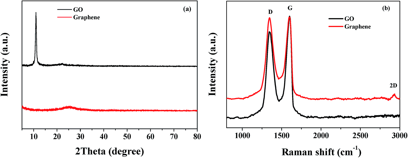 | ||
| Fig. 1 XRD patterns (a) and Raman spectra (b) of GO and graphene. | ||
Fig. 1b shows the Raman spectra of GO and graphene and it could be inferred from Fig. 1b that the carbon framework was structurally changed during the chemical reduction of GO to graphene. The two characteristic peaks located at 1348 cm−1 and 1598 cm−1 in the Raman spectrum of GO are the D band and the G band, respectively. The D band is ascribed to the disorder and defects in the hexagonal lattice, whereas the G band results from the vibration of sp2-bonded carbon atoms in the two-dimensional hexagonal lattice.39 From the Raman spectrum of graphene it can also be seen that the intensity ratio of the D and G bands (ID/IG ratio) is higher than the ID/IG ratio in the Raman spectrum of GO. The changed ID/IG ratio indicates that the average size of the sp2 domains is decreased after the reduction of GO to graphene. All of the results demonstrate that graphene was successfully obtained. What's more, a small 2D peak was observed in the Raman spectrum of graphene at 2935 cm−1, which indicates that graphene with a decreased number of layers was synthesized.40
To further characterize the quality of the synthesized graphene, SEM and TEM were also applied to observe the morphology and structure of the synthesized graphene. As shown in Fig. 2a, a silk-like morphology that is particular to graphene was obtained for the prepared samples, and the wrinkly surface was formed due to the aggregation of graphene sheets, which is further confirmed by the TEM image of graphene (Fig. 2b). From the edge of the prepared graphene shown in Fig. 2b, it is also found that the synthesized graphene was composed of several layers, which is consistent with the results of Raman spectroscopy.
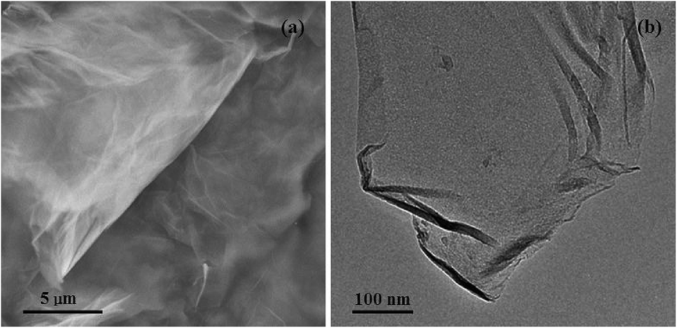 | ||
| Fig. 2 SEM (a) and TEM (b) images of the synthesized graphene. | ||
3.2 Properties of the constructed graphene/TiO2 photoanodes
The Raman spectra of TiO2 and the constructed graphene/TiO2 photoanodes were also recorded to investigate the influence of graphene on the TiO2 film. As shown in Fig. 3, for the constructed graphene/TiO2 photoanodes, the peaks that are ascribed to the anatase TiO2 phase at 143, 194, 398, 512 and 632 cm−1 are also observed. This clearly indicates that the introduction of graphene did not cause the phase transition of TiO2, and this is confirmed by the unchanged peak position of the constructed graphene/TiO2 photoanodes shown in Fig. 3.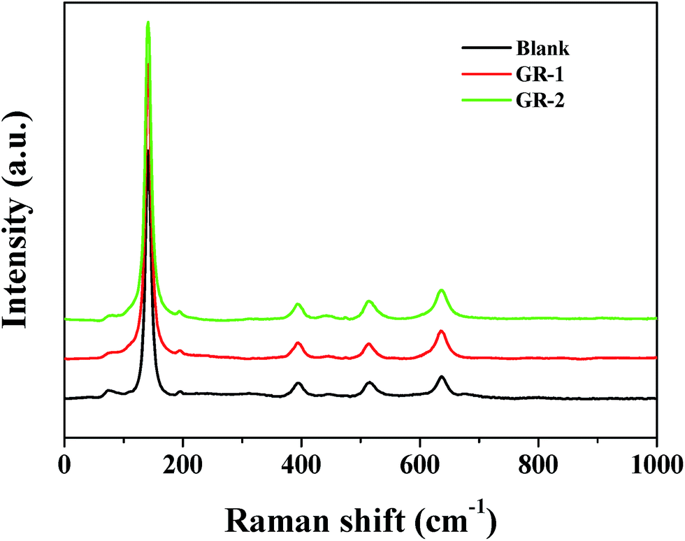 | ||
| Fig. 3 Raman spectra of different photoanodes. | ||
The typical SEM images of different photoanodes are shown in Fig. 4. From the top-view images of the TiO2 films in Fig. 4a, it was seen that many small TiO2 nanoparticles were dispersed randomly on the surface of the FTO glass. Comparatively, top-view images of GR-1 and GR-2 (Fig. 4b and c) showed a porous structure which may be caused by the escape of unreduced graphene or graphene from the surface of the films, and the GR-2 film was composed of more mesopores than those of GR-1. Based on the cross-sectional images of the GR-1 and GR-2 (Fig. 4e and f), the thickness of the GR-1 and GR-2 films was about ca. 12.9 μm, a value comparable to that of pure TiO2 film (Fig. 4d).
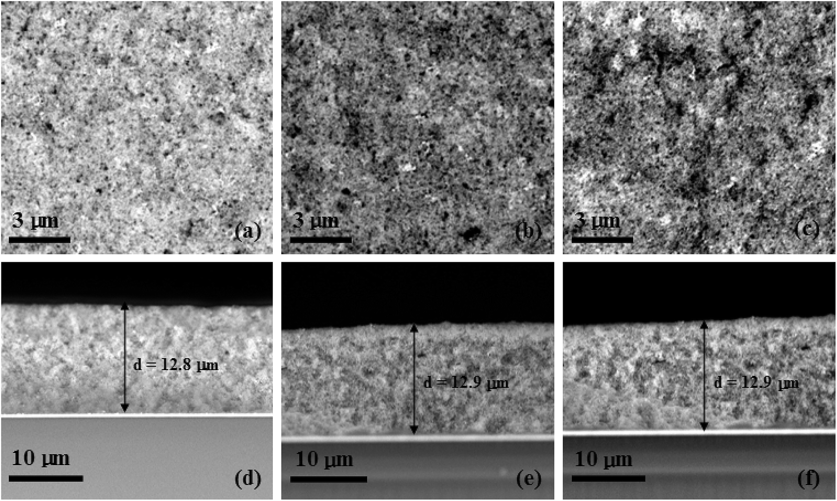 | ||
| Fig. 4 Surface SEM images: (a) TiO2, (b) GR-1, and (c) GR-2 and cross-sectional SEM images: (d) TiO2, (e) GR-1, and (f) GR-2 of different photoanodes. | ||
To further confirm the successful construction of graphene/TiO2 photoanode films, the elemental mapping of Ti and C in GR-1 and GR-2 films was observed. It is found that Ti displays a very homogeneous dispersion in the constructed photoanode films of GR-1 and GR-2 (Fig. 5a and b), indicating that the addition of graphene has little effect on the Ti dispersion. However, the dispersion of C in GR-1 and GR-2 is significantly different. For GR-1, the dispersion of C increased from the top to the bottom of the film which is opposite to that for GR-2 (Fig. 4c and d), revealing that the two types of photoanode films with gradient descent and gradient boost graphene contents were successfully constructed.
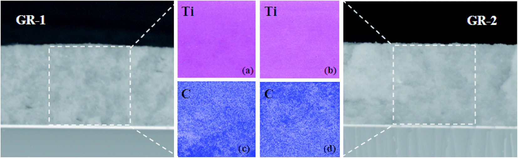 | ||
| Fig. 5 Elemental mapping of Ti (a and b) and C (c and d) in GR-1 (a and c) and GR-2 (b and d) films. | ||
Furthermore, to verify the presence of graphene in the constructed graphene/TiO2 photoanodes, X-ray photoemission spectroscopy (XPS) measurement was carried out on the GR-2 film material. As shown in Fig. 6a, the XPS survey spectra of GR-2 reveal that the Ti 2p, O 1s and C 1s peaks exist for the constructed graphene/TiO2 photoanode, which further indicates that the graphene/TiO2 photoanodes with a gradient graphene content were successfully constructed and graphene was introduced into the graphene/TiO2 photoanodes under the experimental conditions reported here. It could be observed from the C 1s XPS spectra in Fig. 6b that four types of carbon bonds appeared with binding energies of 284.3, 285.8, 287.3, and 288.3 eV corresponding to the sp2 C (C![[double bond, length as m-dash]](https://www.rsc.org/images/entities/char_e001.gif) C, C–C), C–O, CO, and Ti–O–CO, respectively.41,42 The XPS spectra of C 1s confirm the existence of graphene in the constructed photoanode film and the partial binding of graphene with the TiO2 grains in the constructed graphene/TiO2 photoanode.
C, C–C), C–O, CO, and Ti–O–CO, respectively.41,42 The XPS spectra of C 1s confirm the existence of graphene in the constructed photoanode film and the partial binding of graphene with the TiO2 grains in the constructed graphene/TiO2 photoanode.
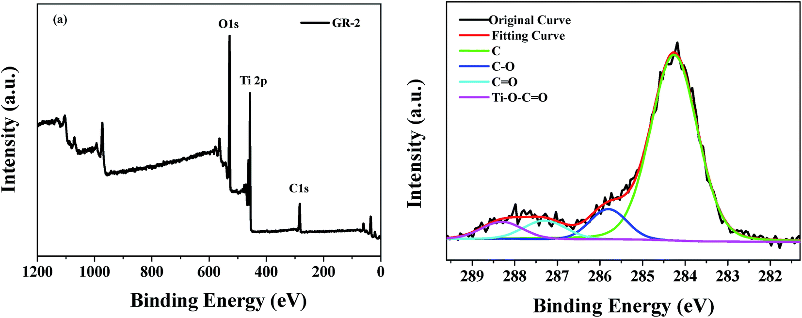 | ||
| Fig. 6 (a) XPS survey spectra of the GR-2 film material, and (b) fine-scanned XPS spectrum in the C 1s region. | ||
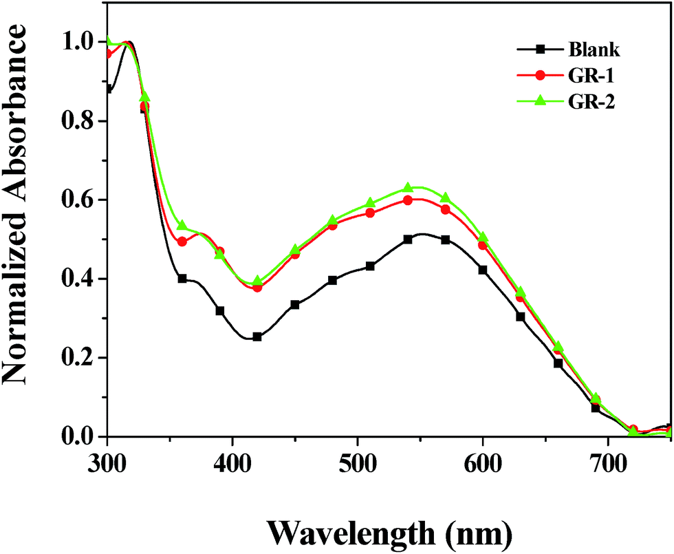
The measurement of the UV-vis spectra of the Blank, GR-1 and GR-2 photoanodes after dye absorption/adsorption was also carried out to investigate the adsorption ability of different photoanodes for light and the N719 dye (Fig. 7). After dye-sensitization, the GR-1 and GR-2 photoanodes showed higher visible-light absorption than the pure TiO2 photoanode (Blank). This clearly indicated that the constructed graphene/TiO2 photoanodes had a higher ability for the effective adsorption of dye, which was very crucial for the enhancement of the energy conversion efficiency in the DSSC system. The greater the amount of graphene in the top layer of the constructed films, the higher the adsorption ability of the photoanode. The adsorption ability of GR-2 is slightly higher than that of GR-1. This is attributed to the fact that a more porous structure was developed on the surface of GR-2 (Fig. 4). The porous structure is beneficial for the diffusion and transfer of dye molecules into the inside of the TiO2 photoanode. Furthermore, it is very helpful for increasing significantly the photoelectric conversion efficiency of the photoanode when more dye molecules are adsorbed on the TiO2 photoanode.
 | ||
| Fig. 7 UV-visible absorption spectra of different photoanodes. | ||
To confirm the different dye loading amounts of Blank, GR-1 and GR-2 photoanodes, the amounts of adsorbed dye on different photoanodes were measured by desorbing the dye from the dye-sensitized films in a 0.1 M NaOH solution in water and ethanol (1:1, v/v). Table 1 shows the measurement results of the dye loading amount and it is found that the amount of dye loading for Blank, GR-1 and GR-2 photoanodes is 1.20 × 10⁻⁷, 1.89 × 10⁻⁷ and 1.95 × 10⁻⁷ mol cm−2, respectively, confirming that the constructed films with a gradient content of graphene are beneficial for the adsorption of dye molecules.
| Photoanodes | Dye loading amount (10−7 mol cm−2) |
|---|---|
| Blank | 1.20 |
| GR-1 | 1.89 |
| GR-2 | 1.95 |
On the other hand, graphene in TiO2 could also act as a light absorber of visible light,43 and the porous structure of graphene/TiO2 could enhance the scattering of light, which would increase the light path inside the photoanode and localize the light inside the photoanode. All of these also resulted in the increase of light absorption.
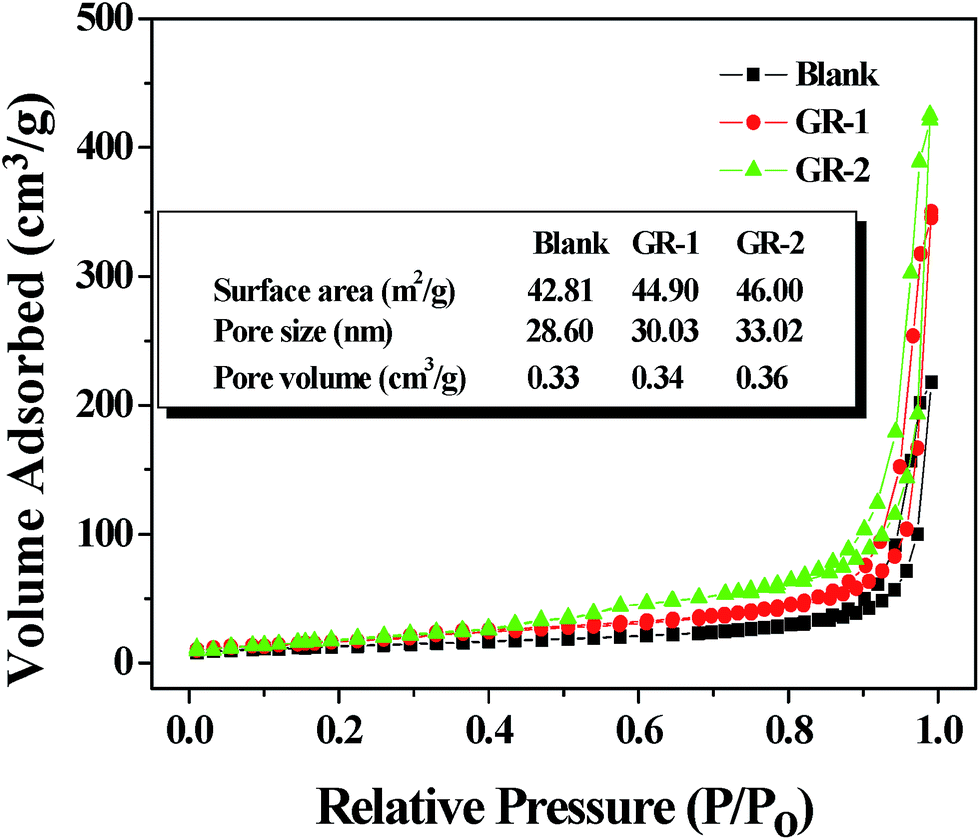
The pore structures of the GR-1 and GR-2 were further characterized using nitrogen adsorption–desorption isotherms, and the results are shown in Fig. 8. According to the Brunauer–Deming–Deming–Teller (BDDT) classification,44 the N2 adsorption–desorption isotherms of Blank, GR-1 and GR-2 shown in Fig. 8 were similar to those of type I in the low pressure range (p/p0 < 0.4), where the isotherm exhibited a high adsorption, indicating the presence of micropores (type I). However, the isotherms of Blank, GR-1 and GR-2 were similar to those of type III in the higher pressure range (p/p0 > 0.4), and the curve exhibited a hysteresis loop in the high relative pressure range of 0.7–1, indicating the presence of mesopores. It can be found from the inset parameters in Fig. 8 that the BET surface areas of GR-1 (44.90 m2 g−1) and GR-2 (46.00 m2 g−1) were higher than that of Blank (42.81 m2 g−1); the pore volumes of the GR-1 and GR-2 were about 0.34 cm3 g−1 and 0.36 cm3 g−1, respectively, which were also larger than that of the blank TiO2 sample (0.33 cm3 g−1); and the pore sizes of GR-1 (30.03 nm) and GR-2 (33.02 nm) were also higher than that of Blank (28.60 nm). These results further confirm that the porous structure was formed by the escape of unreduced graphene or graphene from the surface of the films and it is more obvious for the GR-2 film than that of GR-1.
 | ||
| Fig. 8 Nitrogen adsorption–desorption isotherm and the corresponding parameters of Blank, GR-1 and GR-2 photoanode materials. | ||
To further investigate the effect of graphene on the constructed graphene/TiO2 films, the surface photovoltages (SPS) of different photoanodes which is a well-established contactless technique for surface state distribution were investigated. Fig. 9 shows the SPS of Blank, GR-1 and GR-2 photoanodes. It is found that the surface photovoltage signals between 300 and 750 nm were enhanced by constructing graphene/TiO2 films with a gradient graphene content, which is in the order of GR-2 > GR-1 > Blank. This signal intensity sequence indicates that graphene and its content gradient correlate strongly with the separation of electrons and holes in the photoanodes. The increased dye loading amount and the electronic pathway provided by graphene help to effectively separate photogenerated electrons from the CB of TiO2 films, which resulted in the enhancement of the surface photovoltage signals in the region of 300–750 nm.
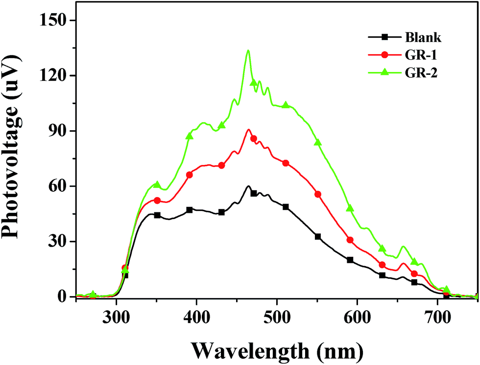 | ||
| Fig. 9 SPS of Blank, GR-1 and GR-2 photoanodes. | ||
3.3 Influence of graphene on the performance of DSSCs
In order to investigate the influence of constructed graphene/TiO2 photoanodes on the performance of DSSCs, the content of graphene in each printed layer of the constructed graphene/TiO2 photoanodes was first optimized based on the characterization of different photoanodes and the optimum photoanodes of GR-1 and GR-2 were finally prepared and applied to assemble DSSCs for testing. The photovoltaic performance of DSSCs based on Blank, GR-1 and GR-2 photoanodes was investigated under a simulated solar irradiation of 100 mW cm−2 (AM 1.5 G). The photocurrent density–photovoltage (J–V) characteristic curves of DSSCs based on Blank, GR-1 and GR-2 photoanodes are shown in Fig. 10. Some critical photovoltaic parameters such as the short-circuit photocurrent density (Jsc) and the open-circuit voltage (Voc) are examined according to the curves in Fig. 10. As interpreted in the experimental section, the power conversion efficiency (η) and the fill factor (FF) of DSSCs can also be obtained accordingly. All of these photovoltaic parameters are summarized in Table 2. It is found that the device without graphene exhibited an η value of 5.45% (with Jsc = 12.63 mA cm−2, Voc = 0.69 V, and FF = 0.62), and the GR-1 and GR-2 devices based on the constructed TiO2 films with a gradient graphene content exhibited an η value of 6.82% (with Jsc = 15.54 mA cm−2, Voc = 0.71 V, and FF = 0.62) and 7.71% (with Jsc = 17.11 mA cm−2, Voc = 0.72 V, and FF = 0.63), respectively. It is obvious that the use of graphene in TiO2 films by constructing graphene/TiO2 photoanodes with a gradient graphene content significantly improved the power conversion efficiency of the devices. This is because these graphene/TiO2 photoanodes could enhance the dye loading amount and improved the light utilization efficiency. Meanwhile, the introduction of graphene with a gradient content in graphene/TiO2 films could enhance the electron bridge effect of graphene in DSSCs, which could provide an effective and fast electron transport pathway, resulting in enhanced electron transport and suppressed charge recombination, and hence improved photovoltaic performance of DSSCs. This effect will be further discussed in the next part.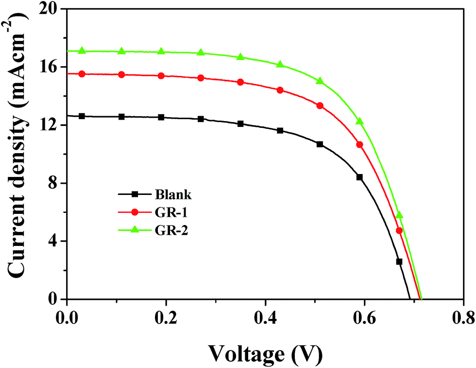 | ||
| Fig. 10 J–V curves of the DSSCs based on different photoanodes. | ||
| Photoanodes | J sc (mA cm−2) | V oc (V) | FF | η (%) | Ref. |
|---|---|---|---|---|---|
| Blank | 12.63 | 0.69 | 0.62 | 5.45 | This work |
| GR-1 | 15.54 | 0.71 | 0.62 | 6.82 | This work |
| GR-2 | 17.11 | 0.72 | 0.63 | 7.71 | This work |
| G-0.25 | 14.02 | 0.71 | 0.61 | 6.03 | 45 |
| G-0.5 | 14.89 | 0.71 | 0.60 | 6.33 | 45 |
| G-1.0 | 15.23 | 0.71 | 0.62 | 6.69 | 45 |
| G-1.5 | 15.10 | 0.71 | 0.60 | 6.37 | 45 |
| G-2.0 | 14.41 | 0.69 | 0.58 | 5.73 | 45 |
| G-2.5 | 12.88 | 0.66 | 0.57 | 4.90 | 45 |
Additionally, the GR-2 device exhibited more excellent performance compared with the GR-1 device, indicating that the order of the gradient graphene content in photoanodes could also affect the performance of DSSCs. As discussed above, there was a greater amount of graphene in the top layer of the constructed GR-2 film. Therefore, the GR-2 film was composed of more mesopores than the GR-1 film due to the escape of unreduced graphene or graphene from the surface of the films. The porous structures help dye molecules to transfer and diffuse into the inside of the TiO2 photoanode easily. Therefore, GR-2 loads a greater amount of dye than GR-1. What's more, the more porous structure of GR-2 could scatter more light, localize more light inside the photoanode, and increase the light path inside the photoanode, which will finally result in better performance compared with GR-1.
What's more, these constructed graphene/TiO2 photoanodes with a gradient graphene content also show better performance than the graphene/TiO2 photoanodes with a constant graphene content which were previously reported by our group.45 A comparison of the results of different photoanodes is provided in Table 2. As shown in Table 2, the constructed graphene/TiO2 photoanodes with a gradient graphene content (both GR-1 and GR-2) show much better performance than the graphene/TiO2 photoanodes with any constant graphene content. These compared results further confirmed that the construction of graphene/TiO2 photoanodes with a gradient graphene content could further enhance the effect of graphene on TiO2 photoanodes.
3.4 Optical and electrochemical characteristics of DSSCs
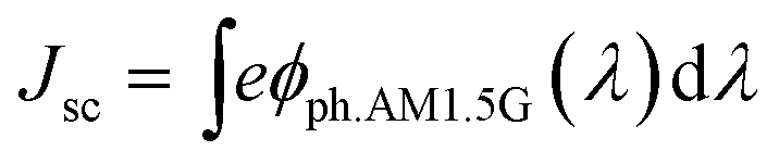
The higher η values of GR-1 and GR-2 compared with the blank device are mainly caused by the enhanced photovoltaic parameters of Voc and Jsc. In particular, the enhanced Jsc value is ascribed to the enhanced IPCE response of the cell, since they are related by the equationwhere e is the elementary charge and ϕph.AM1.5G is the photon flux at AM 1.5.46Fig. 11 shows the IPCE spectra of DSSCs based on different photoanodes. The blank device shows a broad IPCE spectrum from 400 to 750 nm, which is enhanced when graphene is introduced into the constructed films. This further confirms that there was a significant synergistic effect between graphene and TiO2 on light harvesting, electron injection and collection. Based on the absorption spectra and the IPCE spectrum, the cell's higher Jsc in the case of the constructed graphene/TiO2 photoanodes is mainly attributed to better light harvesting due to an increased dye loading amount, and enhanced electron transport through a fast and effective electron transport pathway provided by graphene.
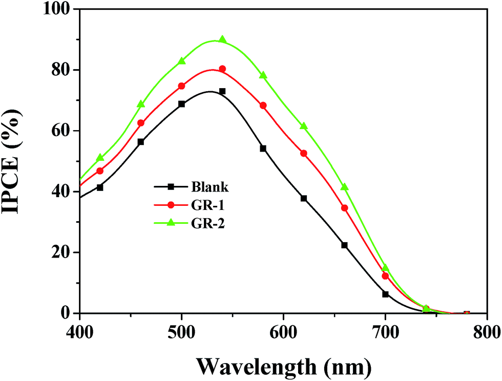 | ||
| Fig. 11 IPCE spectra of the DSSCs based on different photoanodes. | ||
Furthermore, the electrochemical impedance spectra (EIS) of different devices were measured under standard AM 1.5 G solar irradiation and in the dark with a forward bias of −0.75 V, and a physical model has been proposed to gain quantitative information on the transport/recombination processes.47 The equivalent circuit, represented in the inset of Fig. 12, Rs[C1(R1O)](R2Q2), is used to model the DSSCs system, representing interfaces in composite solar cells. The symbols R and C describe a resistance and a capacitance, respectively, Rs is the series resistance, R1 and R2 are the charge transfer resistances, O accounts for finite-length Warburg diffusion (Zw) and Q is the symbol for the constant phase element (CPE).
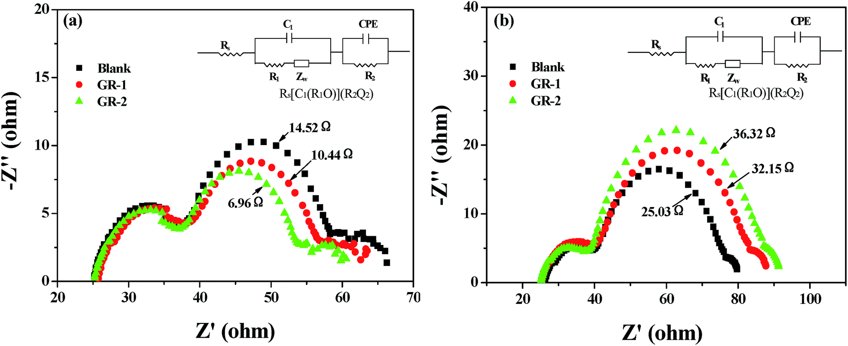 | ||
| Fig. 12 Nyquist plots of DSSCs based on different photoanodes measured (a) under standard AM 1.5 G solar irradiation, and (b) in the dark. | ||
Under light illumination, some electron transport resistance information at the TiO2/dye/electrolyte interface can be obtained by performing the EIS measurement of different devices, and this electron transport resistance information is very important to analyze the improved efficiency of DSSCs.48Fig. 12a shows the Nyquist plots of different devices under illumination, and the three semicircles located in the low, middle and high frequency regions (right to left) are attributed to the charge transfer in the electrolyte (Nernst diffusion), the electron transfer at the TiO2/dye/electrolyte interface and the electrochemical reaction at the Pt/electrolyte interface, respectively.49 It was found from the Nyquist plots that the radius of the large middle frequency semicircle decreased after graphene was introduced into the constructed photoanodes. The decreased radius means a decrease of the electron transfer resistance (Rct) and an increase of the electron transfer rate at this interface. After fitting the curve with the equivalent circuit, it is found that the Rct values are in the order of GR-2 (6.96 Ω) < GR-1 (10.44 Ω) < Blank (14.52 Ω), which indicates that the charge transfer rate increased in the order of GR-2 > GR-1 > Blank after the introduction of graphene, resulting in an increase of the Jsc value.
Meanwhile, under dark conditions, EIS is used to investigate the kinetics of recombination processes in the device with the constructed photoanodes and to understand the enhanced Voc value in different devices. Fig. 12b shows the Nyquist plots of devices based on different photoanodes, and the three semicircles located in the low, middle and high frequency regions (right to left) are attributed to the charge transfer in the electrolyte (Nernst diffusion), the electron transfer at the TiO2/dye/electrolyte interface and the redox reaction at the Pt counter electrode, respectively.49 It was found that the radius of the larger semicircle located in the middle frequency region increases after the constructed photoanodes were used, indicating an increase of back recombination resistance (Rrec). After fitting the curve with the equivalent circuit, it is found that the Rrec values are in the order of GR-2 (36.32 Ω) > GR-1 (32.15 Ω) > Blank (25.03 Ω). A large Rrec means larger resistances of the charge transfer from the TiO2 to the electrolyte, which is beneficial for retarding the charge recombination between injected electrons and I3− ions in the electrolyte, resulting in a smaller charge recombination rate and an increase of the Voc value. Therefore, the Voc values of the devices were also in the order of GR-2 > GR-1 > Blank.
The above results from EIS were confirmed by dark current–voltage (J–V) measurements of different devices. Fig. 13 shows the J–V curves of different devices under dark conditions. It was seen from Fig. 13 that the dark current is lower for the devices with the constructed photoanodes compared with that of the blank device, which is in the order of GR-2 < GR-1 < Blank. The lower dark current in GR-1 and GR-2 indicated that the back reaction of the injected electrons with I3− in the electrolyte was successfully suppressed by graphene via enhancing electron transport, giving rise to Voc and Jsc, resulting in a higher η value. The order of the gradient graphene content was also an important factor that affected the performance of DSSCs.
 | ||
| Fig. 13 Dark current of the DSSCs based on different photoanodes. | ||
The recombination kinetics of the devices based on different photoanodes were further investigated by recording the open-circuit voltage decay (OCVD) curves. Before the OCVD measurement, DSSCs were illuminated with the simulated solar light until a steady-state voltage was obtained. Under these conditions the equilibrium between electron injection and recombination is attained at the FTO surface. After interrupting the illumination, the Voc starts to decay, which reflects the decrease of the electron concentration at the FTO surface caused mainly by the recombination of charges. This means that there is a proportional relationship between the response of the OCVD and the recombination velocity of photoelectrons.50 The OCVD decay curves of devices based on different photoanodes are shown in Fig. 14a. It was found that the OCVD response of DSSCs with the constructed photoanodes was much slower than that of blank DSSCs, especially in the shorter time domain (within 30 s). The correlation between electron lifetime (τe) and Voc decay can be expressed by the following equation:
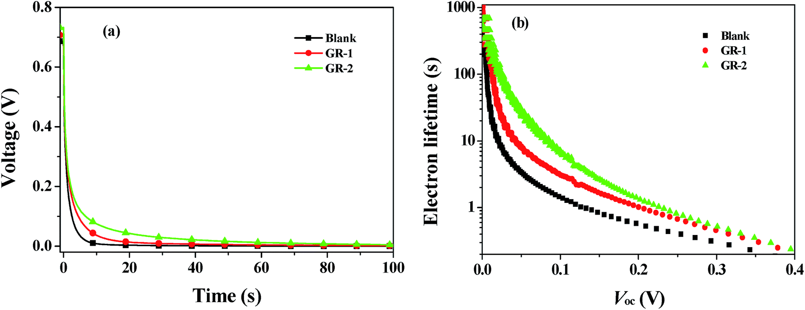 | ||
| Fig. 14 (a) The OCVD curves of the DSSCs with different photoanodes; (b) the electron lifetime as a function of Voc of the DSSCs with different photoanodes. | ||
4. Conclusion
In conclusion, TiO2 photoanodes with a gradient graphene content were constructed to study the influence of graphene on the performance of dye sensitized solar cells. After the construction of the photoanodes with a gradient graphene content, the DSSCs displayed a higher dye loading amount, lower internal resistances, lower charge recombination rate and faster electron transport rate, which resulted in high open circuit voltage and current density. Under the optimum conditions, the DSSC exhibited a Voc of 0.72 V, a Jsc of 17.11 mA cm−2, a FF of 0.63, and an energy conversion efficiency (η) of 7.71%, indicating a 41% increase in η than that of the DSSC based on a pure TiO2 photoanode, which gives a Voc of 0.69 V, a Jsc of 12.63 mA cm−2, a FF of 0.62, and an η value of 5.45%. The construction of photoanodes with a gradient graphene content could really enhance the efficiency of DSSCs by improving the dye loading amount and enhancing the electron bridge effect of graphene from TiO2 to the FTO, which accelerated the electron transport rate and lowered the charge recombination rate. The order of the gradient graphene content also plays an important role in enhancing the performance of DSSCs.Acknowledgements
This work was supported by the National Natural Science Foundation of China (Grant 21571042, 21371040 and 21203058), the National Key Basic Research Program of China (973 Program, 2013CB632900), the Science Foundation for Youths of Heilongjiang Province of China (Grant No. QC2016013), the Foundation of the Educational Commission of Heilongjiang Province of China (No. 12531579), the Innovative Talents Program of the Heilongjiang University of Science and Technology (Q20130202) and the Postdoctoral Foundation of Heilongjiang Province of China (LBH-Z16203).References
- B. O'Regan and M. Grätzel, Nature, 1991, 353, 737–740 CrossRef.
- M. Grätzel, Acc. Chem. Res., 2009, 42, 1788–1798 CrossRef PubMed.
- E. L. Unger, S. J. Fretz, B. Lim, G. Y. Margulis, M. D. McGehee and T. D. P. Stack, Phys. Chem. Chem. Phys., 2015, 17, 6565–6571 RSC.
- T. Abdelhafed, M. Frederic, H. Alexandre, C. J. Christophe, Y. P. Xue and D. Pierre, Sol. Energy Mater. Sol. Cells, 2016, 148, 52–59 CrossRef.
- T. Chen, S. Wang, Z. Yang, Q. Feng, X. Sun, L. Li, Z. S. Wang and H. Peng, Angew. Chem., Int. Ed., 2011, 50, 1815–1819 CrossRef CAS PubMed.
- M. Grätzel, J. Photochem. Photobiol., C, 2003, 4, 145–153 CrossRef.
- X. Fang, M. Li, K. Guo, X. Liu, Y. Zhu, B. Sebo and X. Zhao, Sol. Energy, 2014, 101, 176–181 CrossRef CAS.
- J. van de Lagemaat, N. G. Park and A. J. Frank, J. Phys. Chem. B, 2000, 104, 2044–2052 CrossRef CAS.
- A. Kongkanand, D. R. Martínez and P. V. Kamat, Nano Lett., 2007, 7, 676–680 CrossRef CAS PubMed.
- A. Kongkanand and P. V. Kamat, ACS Nano, 2007, 1, 13–21 CrossRef CAS PubMed.
- M. Adachi, Y. Murata, J. Takao, J. Jiu, M. Sakamoto and F. Wang, J. Am. Chem. Soc., 2004, 126, 14943–14949 CrossRef CAS PubMed.
- M. Kovendhan, D. P. Joseph, P. Manimuthu, S. Sambasivam, S. N. Karthick, K. Vijayarangamuthu, A. Sendilkumar, K. Asokan, H. J. Kim, B. C. Choi, C. Venkateswaran and R. Mohan, Appl. Surf. Sci., 2013, 284, 624–633 CrossRef CAS.
- Y. D. Duan, J. Zheng, M. Xu, X. Song, N. Fu, Y. Fang, X. Zhou, Y. Lin and F. Pan, J. Mater. Chem. A, 2015, 3, 5692–5700 CAS.
- A. R. Tanyi, A. I. Rafieh, P. Ekaneyaka, A. L. Tan, D. J. Young, Z. Zheng, C. Vijila, G. S. Subramanian and R. L. N. Chandrakanthi, Electrochim. Acta, 2015, 178, 240–248 CrossRef CAS.
- M. Y. Yen, M. C. Hsiao, S. H. Liao, P. I. Liu, H. M. Tsai, C. C. M. Ma, N. W. Pu and M. D. Ger, Carbon, 2011, 49, 3597–3606 CrossRef CAS.
- Y. Lai, H. Zhuang, K. Xie, D. Gong, Y. L. Tang, C. L. Sun and Z. Chen, New J. Chem., 2010, 34, 1335–1340 RSC.
- M. Motlak, N. A. M. Barakat, M. S. Akhtar, A. G. Ei-Deen, M. Obaid, C. S. Kim, K. A. Khalil and A. A. Almajid, Chem. Eng. J., 2015, 268, 153–161 CrossRef CAS.
- R. Agarwal, S. Sahoo, V. R. Chitturi, J. D. Williams, O. Resto and R. S. Katiyar, J. Alloys Compd., 2015, 641, 99–105 CrossRef CAS.
- X. Cheng, H. Liu, Q. Chen, J. Li and P. Wang, Carbon, 2014, 66, 450–458 CrossRef CAS.
- N. Yang, J. Zhai, D. Wang, Y. Chen and L. Jiang, ACS Nano, 2010, 4, 887–894 CrossRef CAS PubMed.
- C. H. Ng, H. N. Lim, S. Hayase, I. Harrison, A. Pandikumar and N. M. Huang, J. Power Sources, 2015, 296, 169–185 CrossRef CAS.
- Y. H. Ng, I. V. Lightcap, K. Goodwin, M. Matsumura and P. V. Kamat, J. Phys. Chem. Lett., 2010, 1, 2222–2227 CrossRef CAS.
- R. Nair, P. Blake, A. Grigorenko, K. Novoselov, T. Booth, T. Stauber, N. Peres and A. Gein, Science, 2008, 320, 1308 CrossRef CAS PubMed.
- S. Stankovich, D. A. Dikin, G. H. Dommett, K. M. Kohlhaas, E. J. Zimney, E. A. Stach, R. D. Piner, S. T. Nguyen and R. S. Ruoff, Nature, 2006, 442, 282–286 CrossRef CAS PubMed.
- D. Li and R. B. Kaner, Science, 2008, 320, 1170–1171 CrossRef CAS PubMed.
- Y. Si and E. T. Samulski, Nano Lett., 2008, 8, 1679–1682 CrossRef CAS PubMed.
- G. Williams, B. Seger and P. V. Kamat, ACS Nano, 2008, 2, 1487–1491 CrossRef CAS PubMed.
- X. Fang, M. Li, K. Guo, Y. Zhu, Z. Hu, X. Liu, B. Chen and X. Zhao, Electrochim. Acta, 2012, 65, 174–178 CrossRef CAS.
- B. Tang, G. Hu, H. Gao and Z. Shi, J. Power Sources, 2013, 234, 60–68 CrossRef CAS.
- Z. Xiang, X. Zhou, G. Wan, G. Zhang and D. Cao, ACS Sustainable Chem. Eng., 2014, 2, 1234–1240 CrossRef CAS.
- C. H. Shan, H. Zhan, W. L. Chen, Z. M. Su and E. B. Wang, J. Mater. Chem. A, 2016, 4, 3297–3303 CAS.
- S. B. Kim, J. Y. Park, C. S. Kim, K. Okuyama, S. E. Lee, H. D. Jang and T. O. Kim, J. Phys. Chem. C, 2015, 119, 16552–16559 CAS.
- H. Ding, S. Zhang, J. T. Chen, X. P. Hu, Z. F. Du, Y. X. Qiu and D. L. Zhao, Thin Solid Films, 2015, 584, 29–36 CrossRef CAS.
- H. D. Jang, E. H. Jo, H. Chang, J. Kim and K. M. Roh, Mater. Lett., 2015, 142, 304–307 CrossRef CAS.
- W. N. Song, C. Y. He, W. Zhang, Y. C. Gao, Y. X. Yang, Y. Q. Wu, Z. M. Chen, X. C. Li and Y. L. Dong, Carbon, 2014, 77, 1020–1030 CrossRef CAS.
- P. Y. Reddy, L. Giribabu, C. Lyness, H. J. Snaith, C. Vijaykumar, M. Chandrasekharam, M. Lakshmikantam, J. H. Yum, K. Kalyanasundaram, M. Grätzel and M. K. Nazeeruddin, Angew. Chem., Int. Ed., 2007, 46, 373–376 CrossRef CAS PubMed.
- D. A. Dikin, S. Stankovich, E. J. Zimney, R. D. Piner, G. H. B. Dommett, G. Evmenenko, S. T. Nguyen and R. S. Ruoff, Nature, 2007, 448, 457–460 CrossRef CAS PubMed.
- F. Xu, J. Chen, X. Wu, Y. Zhang, Y. Wang, J. Sun, H. Bi, W. Lei, Y. Ni and L. Sun, J. Phys. Chem. C, 2013, 117, 8619–8627 CAS.
- S. P. Lim, N. M. Huang and H. N. Lim, Ceram. Int., 2013, 39, 6647–6655 CrossRef CAS.
- A. Siokou, F. Ravani, S. Karakalos, O. Frank, M. Kalbac and C. Galiotis, Appl. Surf. Sci., 2011, 257, 9785–9790 CrossRef CAS.
- H. Bai, Z. Liu and D. D. Sun, J. Mater. Chem., 2012, 22, 18801–18807 RSC.
- M. Xing, F. Shen, B. Qiu and J. Zhang, Sci. Rep., 2014, 4, 1–7 Search PubMed.
- D. Joseph, R. Mayhew and I. A. Aksay, Chem. Rev., 2014, 114, 6323–6348 CrossRef PubMed.
- J. Fan, S. Liu and J. Yu, J. Mater. Chem., 2012, 22, 17027–17036 RSC.
- L. G. Wei, S. S. Chen, Y. L. Yang, Y. L. Dong, W. N. Song and R. Q. Fan, RSC Adv., 2016, 6, 100866–100875 RSC.
- A. Hagfeldt, G. Boschloo, L. Sun, L. Kloo and H. Pettersson, Chem. Rev., 2010, 110, 6595–6663 CrossRef CAS PubMed.
- K. Mukherjee, T. H. Teng, R. Jose and S. Ramakrishna, Appl. Phys. Lett., 2009, 012101 CrossRef.
- C. Y. Hsu, W. T. Chen, Y. C. Chen, H. Y. Wei, Y. S. Yen, K. C. Huang, K. C. Ho, C. W. Chu and J. T. Lin, Electrochim. Acta, 2012, 66, 210–215 CrossRef CAS.
- D. Kuang, S. Uchida, R. Humphry-Baker, S. M. Zakeeruddin and M. Grätzel, Angew. Chem., Int. Ed., 2008, 47, 1923–1926 CrossRef CAS PubMed.
- A. Zaban, M. Greenshtein and J. Bisquert, ChemPhysChem, 2003, 4, 859–864 CrossRef CAS PubMed.
| This journal is © The Royal Society of Chemistry 2017 |