
Solution processing of air-stable molecular semiconducting iodosalts, Cs2SnI6−xBrx, for potential solar cell applications†
Byunghong
Lee
 ab,
Anthony
Krenselewski
ab,
Sung Il
Baik
a,
David N.
Seidman
a and
Robert P. H.
Chang
*ab
ab,
Anthony
Krenselewski
ab,
Sung Il
Baik
a,
David N.
Seidman
a and
Robert P. H.
Chang
*ab
aDepartment of Materials Science and Engineering, Northwestern University, Evanston, Illinois 60208, USA
bArgonne-Northwestern Solar Energy Research Center, Northwestern University, Evanston, Illinois 60208, USA
First published on 20th March 2017
Abstract
Organic–inorganic hybrid lead-based perovskite solar cells have already achieved high performance efficiency (∼20%). A major challenge with these cells, however, is their stability and environmental safety concerns due to the presence of lead. This article reports an effort to develop a new class of tin-based and air-stable molecular semiconducting iodosalts, for potential solar cell applications. The compounds are Cs2SnI6−xBrx for a range of x that provides the desired bandgaps from ∼1.3 eV to ∼2.9 eV with x < 3 being suitable for solar cell design. The Sn in this compound is in the 4+ oxidation state, and thus it is much more stable with respect to oxidation and more resistant to hydrolysis during processing and device operation. The focus of this article is on the detailed synthesis challenges in the solution processing of these compounds. A two-step solution synthesis method has been developed whereby during Step-1 a well-defined CsI crystalline film was formed for the appropriate chemical reaction with a solution of SnI during Step-2. By careful tuning of each step of the process and with the use of detailed structural, electrical and optical characterization as feedback, a series of Cs2SnI6−xBrx films were produced. The importance of having a stoichiometric compound for optimal performance of the material was revealed during solar cell fabrication. For the purpose of demonstrating a solar cell device assembly, a sandwich-type photochemical cell with an all solid state ionic conductor blended with inorganic materials and succinonitrile was employed for easy processing to obtain stable results. The cells show a conversion efficiency of 2.1% for the case of the x = 2 compound.
1 Introduction
The interest in the use of organic–inorganic hybrid perovskite compounds for application in solar cells has been primarily due to the rapid surge in cell efficiency to ∼20% during the past several years.1–6 Most of the perovskite compounds under investigation by community are based on APbI3 structures, where A can be Cs, methylamonium (CH3NH3+) or formamidinium (HC(NH2)2+).7–10 These perovskites exhibit long term instabilities associated with phase transitions, ambient hydrolysis, and photo-degradation, while the presence of a water-dispersible form of lead in solar cells and the presence of toxic additives in their hole transport layers raises environmental concerns.11–13 The fabrication of tin based ASnI3 perovskite cells has been demonstrated but these materials exhibit even greater instabilities along with phase transitions and lower Voc values. Thus, to realize commercial applications of this technology it is important to achieve analogous optical and photovoltaic performance using lead-free, toxic-additive-free, and air-stable compounds for ambient processing. Therefore, the use of a new class of environmentally benign materials with intrinsic stability and possessing beneficial optoelectronic performance can be an alternative to the current approach.In an earlier article we demonstrated the use of Cs2SnI6 as a hole conductor in a dye sensitized solar cell.14 In the Cs2SnI6 iodosalt compound, the Sn is in the 4+ oxidation state, and much more stable with respect to oxidation and hydrolysis during device processing and operation. Cs2SnI6 is a direct bandgap (∼1.3 eV) semiconductor, and depending on doping, it can be either an n- or a p-type semiconductor suggesting an ambipolar nature of this compound.14
This paper is structured into three major parts: in Section 1, a detailed discussion on the ramifications of material structure and chemistry related challenges is presented for solution processing, along with careful characterization. To prepare for device fabrication, in Section 2, we discuss band alignment engineering among the solar cell layers to optimize the final device performance. Finally, in Section 3, we present a unique device configuration and its performances.
2 Results and discussion
2.1. Optimization of the two-step solution processes for Cs2SnI6 thin films
The focus of this section is the discussion of a series of experiments describing how we have optimized our two-step solution processes for synthesizing iodosalt Cs2SnI6−xBrx thin films to achieve suitable properties as solar photon absorbers for light to charge conversion. Our results are organized into three sections: Section 1.1 describes the thin-film optimization of the x = 0, Cs2SnI6, iodosalt. In Section 1.2 we focus on Step-1, the morphological control of the CsI film. In Section 1.3, the effects of unreacted CsI in Cs2SnI6 films are presented. Finally, in Section 1.4, we discuss Step-2 of the process where we show how we determine the optimal temperature and duration of the chemical reaction for the second step in an attempt to achieve stoichiometry for the final film.The first step in solution-preparation of Cs2SnI6 thin films was to optimize the processing conditions in order to obtain systematic and reproducible results. We then proceeded to characterize the properties of the films during and after synthesis. It should be noted that many basic parameters such as temperature, time, spatial uniformity, and chemical reactivity are interdependent in our solution processing steps. For device fabrication, both local non-stoichiometric regions (at the nanoscale) and interfacial recombination sites needed to be minimized. This includes (external and internal) surface dangling bonds. The solar cell performance was further optimized by improving the band gap alignment between the TiO2 photo-anode and photon-absorber. To this end we determined the optimum amount of Sn doping in TiO2. The nominal open circuit voltage, Voc, of the cells using Cs2SnI6 is ∼0.26 eV. In order to increase this value, we introduced an appropriate amount of bromide in the form of Cs2SnI6−xBrx to obtain a Voc of 0.58 eV for the case of Cs2SnI4Br2. We discuss the device characteristics in terms of performance, stability and reproducibility and give examples of how to fabricate iodosalt based solar cell devices by circumventing costly materials and processing steps.
![[3 with combining macron]](https://www.rsc.org/images/entities/char_0033_0304.gif) m) with a lattice parameter a of 11.6276(9) Å and consisted of discrete, regular {SnI6}2− octahedra and Cs+ cations (K2PtCl6 structure type). The crystal structure (Fig. 1b right) can be described as a defective variant of the perovskite CsSnI3, where half of the Sn sites are vacant (i.e. A2SnX6), resulting in a Werner-like coordination complex.15,16 The +4 oxidation state of Sn in Cs2SnI6 leads to its intrinsic stability. In addition, Fig. 1c shows the differences in the surface and cross-sectional morphologies in the Cs2SnI6 compound when CsI layers (from drop-coating and E-spray coating) were soaked in SnI4 solution and dried. We note that in the case of E-sprayed CsI coating, the formed Cs2SnI6 compound has a smoother surface and interfaces as shown in Fig. 1c. This was verified by using a surface profilometer (Dektak 150, Veeco Metrology Inc) with a 3D interactive display indicating large thickness variations across the drop coated film as compared with a smoother surface of the E-sprayed film. In addition, we observed much less compaction of the drop coated film compared to that of the E-sprayed sample as seen from the SEM cross section in the lower frames of Fig. 1c.
m) with a lattice parameter a of 11.6276(9) Å and consisted of discrete, regular {SnI6}2− octahedra and Cs+ cations (K2PtCl6 structure type). The crystal structure (Fig. 1b right) can be described as a defective variant of the perovskite CsSnI3, where half of the Sn sites are vacant (i.e. A2SnX6), resulting in a Werner-like coordination complex.15,16 The +4 oxidation state of Sn in Cs2SnI6 leads to its intrinsic stability. In addition, Fig. 1c shows the differences in the surface and cross-sectional morphologies in the Cs2SnI6 compound when CsI layers (from drop-coating and E-spray coating) were soaked in SnI4 solution and dried. We note that in the case of E-sprayed CsI coating, the formed Cs2SnI6 compound has a smoother surface and interfaces as shown in Fig. 1c. This was verified by using a surface profilometer (Dektak 150, Veeco Metrology Inc) with a 3D interactive display indicating large thickness variations across the drop coated film as compared with a smoother surface of the E-sprayed film. In addition, we observed much less compaction of the drop coated film compared to that of the E-sprayed sample as seen from the SEM cross section in the lower frames of Fig. 1c.
 | ||
| Fig. 1 (a) SEM images of CsI films produced by different routes: spin coating deposition (1500 rpm, 30 s), dropping deposition and E-spray deposition. (b) Sequential solution-based deposition process for Cs2SnI6 films with photo images for each process and the crystal structure of Cs2SnI6 from the VESTA program (top: polyhedral and bottom: wireframe). (c) Thickness profiler (inset: 3D interactive display) and cross-sectional images of the Cs2SnI6 film used by the drop coating and E-spray coating techniques. | ||
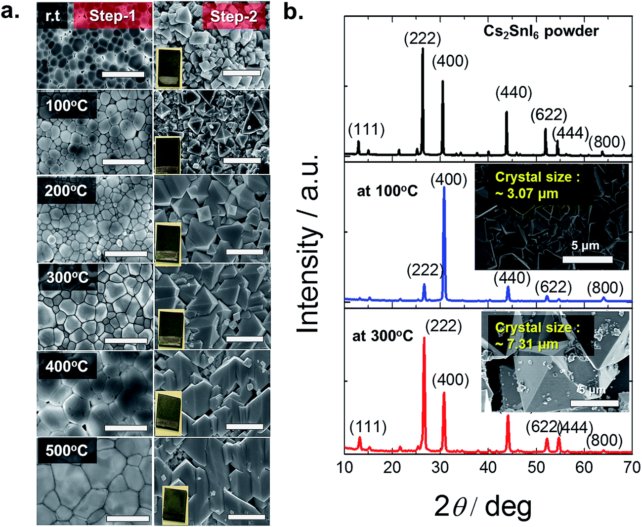 | ||
| Fig. 2 (a) Left column – SEM images of the E-sprayed CsI films annealed at different temperatures in air for 30 min. Corresponding right column—after the addition of SnI4 solution at 110 °C for 20 min Cs2SnI6 films were formed. The scale bar is 5 μm. (b) XRD analysis of Cs2SnI6 powder and from two different CsI annealed films at 100 °C and 300 °C. | ||
A more detailed cross-sectional microstructural analysis investigation was carried out to learn how much of the CsI was converted to Cs2SnI6 in the thin films. A dual beam focused ion beam (FIB) microscope (Helios Nanolab, FEI Co.) was used to prepare cross-sectional SEM and scanning transmission electron microscopy (STEM) samples utilizing a Ga+ ion. A Pt coating was applied to protect the surface during the microscopy study. The sample was thinned by Ga+ ion etching in a FIB microscope employing a final energy of 2 kV at 24 pA. Fig. 3 displays the cross-sectional SEM and STEM images in the two differently annealed samples in Step-1, CsI annealed at 100 °C (a, b) and at 300 °C for 30 minutes (c and d). The same Step-2 was adopted for both samples: SnI4 solution treated at 110 °C for 20 min. Fig. 3(a and b) show the three different layers (labeled part-a, -b and -c) in the deposited film. The selected area diffraction patterns (SADPs) on the left side of the STEM, Fig. 3b, show that the three parts have different crystallographic structures: part-a is a Cs2SnI6 structure, part-b is a mixed structure of Cs2SnI6 and CsI, and part-c is a CsI structure. On the other hand, for the higher annealing temperature at 300 °C in Step-1, Fig. 3(c and d), the cross-sectional images of SEM and STEM show two crystalline layers, part-a and part-b. The CsI structure in part-a is not present in this sample. This indicates that in the case of 100 °C, the reaction in Step-2 was taking place much slower than that at 300 °C. In addition, as mentioned earlier, unlike the 300 °C case, the 100 °C annealed film is not fully converted into Cs2SnI6. Fewer voids are observed at the interface between the film and the substrate for the 300 °C annealed case. As shown in Fig. 3 a and c, the crystal morphologies are quite different between the two cases. The morphology for the 300 °C case is much more uniform, providing direct evidence that the conversion of CsI to Cs2SnI6 is facilitated by high temperature annealing. The orientation change in the two samples is also displayed in the SADP analyses. The (004) plane is close to the plane normal to the film in the 100 °C annealed sample, SADPs in part-a, whereas, the (222) plane is close to the plane normal to the film in the 300 °C annealed sample, SADPs in part-a of Fig. 3d. This result corresponds to XRD analysis in Fig. 2. Finally, for the case of 300 °C annealing, we still observe a mixture of Cs2SnI6 and CsI near the interface with TiO2 (Fig. 3c and d)
 | ||
| Fig. 3 Cross-sectional scanning electron microscopy (SEM) and scanning transmission electron microscopy (STEM) analyses. (a) SEM and (b) STEM analyses of CsI films annealed at 100 °C in air for 30 minutes (Step-1), and SnI4 solution treated at 110 °C for 20 minutes (Step-2). (c) SEM, and (d) STEM analyses of CsI films annealed at 300 °C in air for 30 minutes with Step-2 being the same. Corresponding selective area diffraction patterns (SADPs) in the three layers (part-a, -b, and -c) are displayed on the left side of the STEM image. Different parts of the films are produced at different annealing temperatures of CsI films in Step-1 (part-a describes the diffraction pattern of crystalline Cs2SnI6, part-b is the mixed structure of Cs2SnI6 and CsI, and part-c is the CsI structure). | ||
 | ||
| Fig. 4 (a) SEM images of the controlled Cs2SnI6 film for studying the effect of remaining CsI in Cs2SnI6 films and (b) photo image of the film: completely (left) and incompletely (right) converted Cs2SnI6 films. | ||
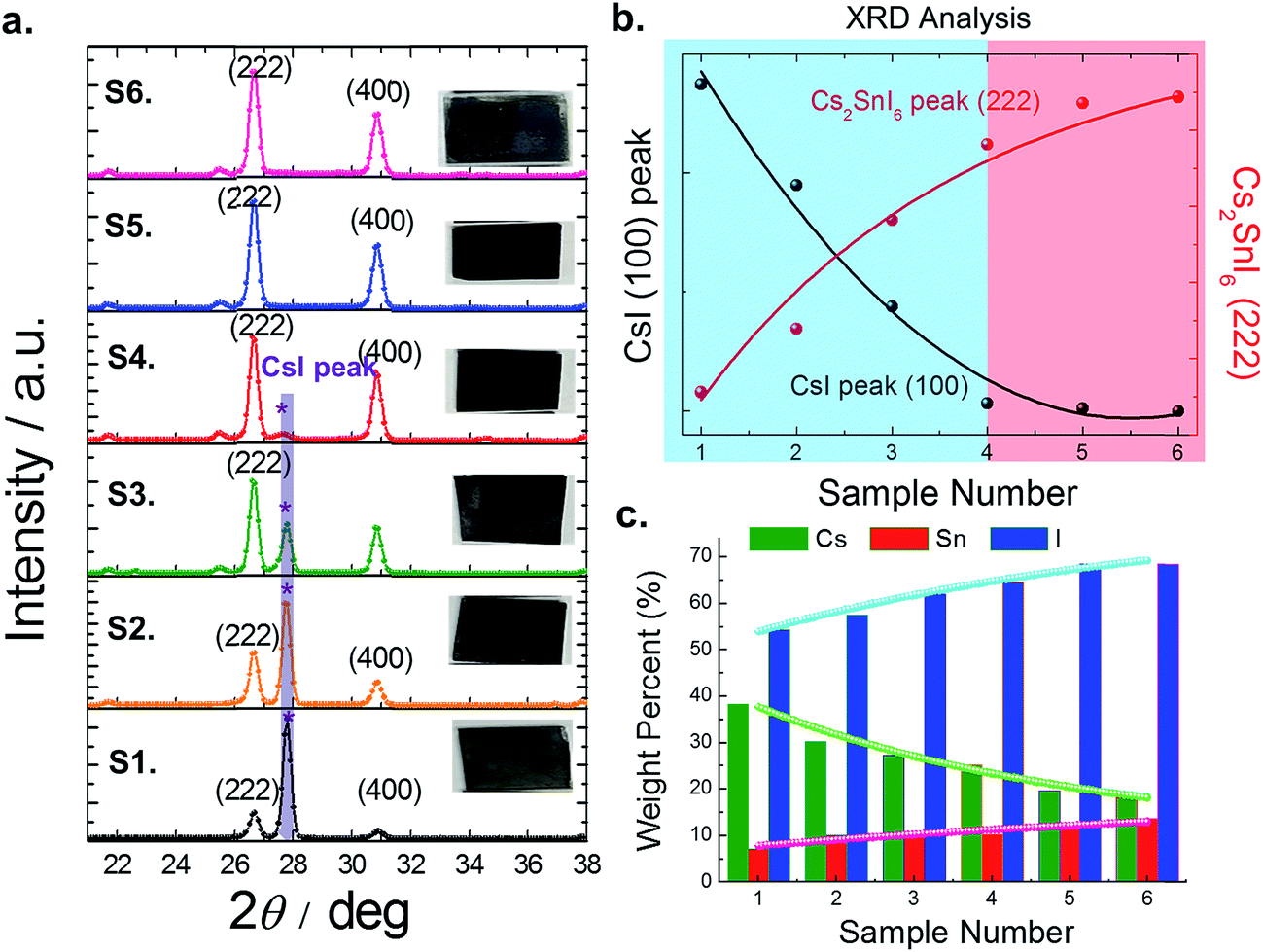 | ||
| Fig. 5 (a) XRD analysis of the controlled Cs2SnI6 film for studying the effect of remaining CsI in Cs2SnI6 films. (b) Graph showing CsI and Cs2SnI6 peak intensity (the presence of the CsI peak (blue) and no CsI peak (red)). (c) EDS data for the elemental analysis (Cs, Sn and I). | ||
| Sample | Int.I (cps deg) | Composition region | EDS (at wt%) | E g | Carrier concentration (×1015 cm−3) | Mobility (cm2 V−1 s−1) | |||||
|---|---|---|---|---|---|---|---|---|---|---|---|
| CsI (110) | Cs2SnI6 (222) | CsI/Cs2SnI6 | Cs | Sn | I | Cs/Sn | |||||
| S1 | 2515(32) | 673(27) | 3.736 | CsI-rich | 38.4 | 7.25 | 54.35 | 5.296 | 1.41 | 4.07 × 10¹⁶ | 1.779 |
| S2 | 1707(16) | 535(12) | 3.191 | CsI-rich | 30.24 | 10.18 | 57.48 | 2.970 | 1.37 | 3.85 × 10¹⁶ | 2.119 |
| S3 | 950(18) | 1627(24) | 0.584 | CsI-poor | 27.29 | 10.8 | 61.97 | 2.527 | 1.35 | 9.88 × 10¹⁵ | 4.812 |
| S4 | 99(9) | 1332(16) | 0.074 | Mostly Cs2SnI6 | 25.16 | 10.25 | 64.59 | 2.455 | 1.32 | 1.14 × 10¹⁴ | 9.072 |
| S5 | — | 1983(28) | 0.000 | Cs2SnI6 | 19.65 | 11.82 | 68.53 | 1.662 | 1.30 | 4.86 × 10¹³ | 10.59 |
| S6 | — | 2006(27) | 0.000 | Cs2SnI6 | 18.1 | 13.64 | 68.26 | 1.327 | 1.28 | 1.51 × 10¹⁵ | 2.312 |
The optical absorption spectra of each film were measured with a UV-visible spectrophotometer (Perkin Elmer LAMBDA 1050) in the wavelength range of 250–1200 nm (see Fig. 6a). Earlier, our study showed that Cs2SnI6 had a direct band gap of ∼1.3 eV at the Γ point.14 However, Cs2SnI6 crystals exhibit dispersive conduction band states due to intrinsic defects, causing an argument over the bandgap energy value.18–20 In our experimental study here using the six samples discussed above, and using EDS and XRD analysis, we now confirm that the presence of CsI in a Cs2SnI6 film can influence its bandgap (see Fig. 6b). With an increase in the percentage of CsI in Cs2SnI6, the absorption edge shifted to shorter wavelengths. The band gap of the completely reacted Cs2SnI6 film is consistent with our earlier calculation, while Cs2SnI6 films containing a high amount of CsI impurities show an increased band gap of about 0.1 eV. In our experimental observation, the carrier concentrations in these samples (at the 1.5 μm thickness) ranged from 4.86 × 1013 cm−3 to 4.07 × 1016 cm−3 and mobility ranged from 1.779 cm2 V−1 s−1 (at 1.4 eV) to 10.59 cm2 V−1 s−1 (at 1.3 eV) (see Table 1).
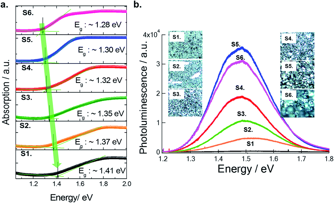 | ||
| Fig. 6 (a) Bandgap calculation of the controlled Cs2SnI6 film for studying the effect of remaining CsI in Cs2SnI6 films, (b) Photo-luminescence (PL) analysis for each sample with confocal microscopy images. | ||
Photo-luminescence (PL) measurement can further confirm the levels of CsI in the Cs2SnI6 films. At room temperature, we observed an increased PL intensity and red-shifted PL position with decreasing amount of CsI in Cs2SnI6 crystals following the same trend as the band gap. For example, in the case of a completely reacted Cs2SnI6 film (S5), the intensity of the PL peak at 1.48 eV increases by ∼10 times and the peak position shifts to a lower energy by ∼20 meV as compared with S2. Therefore, we can appreciate that it is necessary to avoid the unreacted CsI, which leads to undesired optical and electrical properties in Cs2SnI6 films.
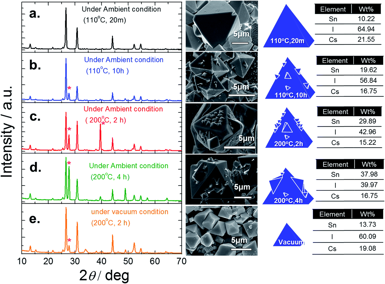 | ||
| Fig. 7 XRD analysis and SEM images with EDS of Cs2SnI6 films under different time and temperature treatment conditions of Step-2 with SnI4 solution (a) at 110 °C for 20 min, (b) 110 °C for 10 hours, (c) 200 °C for 2 hours, and (d) 200 °C for 4 hours in an ambient system and (e) 200 °C for 2 hours under vacuum (10−4 torr). | ||
To confirm this sublimation, we took two similar fresh films and annealed one in air and the other in a vacuum at 200 °C for 4 h. As seen in Fig. 7d, the film annealed in air exhibits growth of nanoparticles on the Cs2SnI6 surface, while the sample annealed in a vacuum retained its smooth surface, Fig. 7e. XRD measurements show the differences between these two samples: the sample annealed in a vacuum maintained the Cs2SnI6 structure, containing only a small amount of CsI, while the sample annealed in air contains pronounced extra peaks from the presence of CsI crystallites due to the partial removal of SnI4 during the annealing process. Local EDS measurements performed with a focused electron beam also confirmed that the vacuum sample maintained its Cs2SnI6 composition. Furthermore, the elemental ratio of crystals with different sizes was consistent with a Cs2SnI6 composition. Thus, due to the water vapor in air (50–75% humidity, typically in our lab), we expect a significant degree of hydrolysis reaction to take place under the employed experimental conditions (200 °C for 4 h). Under these conditions, and owing to the relatively weak bonding between Sn and I, SnO2 crystallites can be formed on the Cs2SnI6 surfaces. These studies led us to conclude that for Step-2, the optimal processing conditions were 110 °C for 20 minutes.
2.2. Interfacial bandgap engineering
While the performance of the sensitizer layer is very important in a solar cell, the charge transport layers, their interfaces, and the electrodes that connect the device to the outside world are important as well. In this section we report how we have improved two interfacial junctions: (a) between nano-porous TiO2 and Cs2SnI6, by reducing the bandgap of the TiO2 through doping with Sn to improve electron transfer between the layers, and (b) the optimization of the bandgap of the sensitizer layer, so as to approach the ideal value of 1.4 eV (using an AM 1.5 solar spectrum) for a solar cell made from a single material.22 The 1.3 eV bandgap of Cs2SnI6 can be increased through incorporation of Br into the Cs2SnI6 crystal structure.18 In section 2.2, we discuss our results for Cs2SnI6−xBrx films with different values of x.Fig. 8a shows the X-ray diffraction patterns of the TiO2 and TiO2 with different concentrations of doped Sn. With Sn contents above 2 wt%, the rutile (110) peak starts to progressively increase, whereas the anatase (101) peak diminishes. The surface morphologies of the undoped E-sprayed TiO2 and SnO2 films are shown in Fig. 8b. It can be seen that the undoped E-sprayed TiO2 is made mostly of spherical structures, while E-sprayed SnO2 shows flower-like structures with a relatively rough surface. The Eg of the TiO2 was calculated from indirect transitions (n = 1/2) and Fig. 8c shows the plots of (αhv)1/2versus hv. A perfect fit was obtained for all the samples giving the values of 3.22 eV for the bare TiO2 film, 3.07 eV for 2 wt% Sn–TiO2, and 2.98 eV for 5 wt% Sn–TiO2. Ultraviolet photoemission spectroscopy (UPS) measurements are also performed to determine the VBM. The substitution of Sn for Ti does not shift the VBM. As a result, from the observation of the band gap with varying concentration of doped Sn and EVB values, the CBM can be estimated to be −4.35 eV for 2 wt% Sn in TiO2 and −4.44 eV for 5 wt% Sn in TiO2, which are 0.15 eV and 0.24 lower than that of the ECB of pure TiO2 (−4.2 eV versus vacuum). Therefore, modification of the electron transport medium is expected to improve the electron injection from Cs2SnI6−xBrx materials.
 | ||
| Fig. 8 (a) XRD patterns (anatase phase labeled A, rutile R and Sn S) and (b) band gap calculation (the insets show the schematic band diagram and the surface morphologies – the scale bar is 500 nm) for the different Sn doping concentrations. | ||
| (1 − x)CsI + xCsBr + SnX4 (X = I, Br) → Cs2SnI6−xBrx |
The X-ray diffraction patterns of the films thus prepared are shown in Fig. 9a. As the Br composition is gradually increased, the angle of the main peak of the (222) plane is shifted from 26.53° to 28.45°. The measured band gaps of the Cs2SnI6−xBrx films with varying substitution of Br are shown in Fig. 9b. From diffuse reflectance UV-vis-near IR measurements, we note that in this particular system, the band gap of Cs2SnBr6 is 2.9 eV, drastically different from that of Cs2SnI6 (1.3 eV). This contrasts with the much smaller difference in the band gap between CsSnBr3 (1.7 eV) and γ-CsSnI3 (1.3 eV) which is only 0.4 eV. From both XRD and optical analyses, the two-step process produced films are indeed modified by the partial halide substitution and this can be clearly observed in the measured emission (PL) which shows a clear blue shift as Br− is incorporated into the Cs2SnI6 matrix, while the intensity of the PL peak diminished with increasing Br ratio (see Fig. 9b bottom). In this graph, the intensity was normalized so that increasing noise level indicates a weaker signal. This observation constitutes an important indication that these materials can be successfully utilized as light absorbers in solar cells. The shift in the position of energy levels can be also confirmed by UPS analysis (see ESI 2†). It is noted that the Cs2SnI6 film shows the highest HOMO position at 5.40 ± 0.09 eV. By increasing the ratio of Br, there is a clear downshift of the HOMO level from 5.61 ± 0.08 eV to 6.78 ± 0.9 eV and this result is consistent with reports on analogous HOMO level shifts of CH3NH3PbI3.4,30 Furthermore, with the increase of Br composition, the color of the Cs2SnBrxI6−x films changed from dark brown to brown/red, and then to light yellow due to the widening of the bandgap, Fig. 9b. For detailed information, the lattice parameter and band gap of the Cs2SnI6−xBrx films are listed in Fig. 10. The obtained films were indeed found to form the Cs2SnI6−xBrx phases as evidenced by small changes in the lattice constant, indicating incorporation of Br− into the Cs2SnI6 lattice or incorporation of I− into the Cs2SnBr6 lattice. Unlike the CsSnI3−xBrx solid solution, the experimental band gap trend of Cs2SnI6−xBrx does not follow the characteristic Vegard's law but instead it increases steadily up to x ∼ 4 followed by an abrupt increase for x > 4 (see Fig. 10). The anomalous nature of the band gap may reflect on the molecular nature of the compounds which may be ascertained to be a random distribution of heterohalide octahedra throughout the solid. Another remarkable result obtained from these experiments lies in the crystallite morphology. SEM analysis indicates that the particle size is significantly reduced upon increasing the Br content in Cs2SnI6−xBrx with the pure Cs2SnI6 in octahedral crystallites with size around ∼1 micron whereas the pure Cs2SnBr6 has smaller (∼300 nm) crystallites of cubic shapes (Fig. 10). This morphology transformation from octahedra to cubes can be explained by the enhanced symmetry.4 Following this trend, the morphology and size of the intermediate Cs2SnI6−xBrx compositions lie in between these two extremes.
 | ||
| Fig. 9 Characteristics of the different compositions of Cs2SnI6−xBrx: (a) XRD patterns of the film from the two-step solution-based deposition process with varying substitutions of Br (CsI and CsBr) and reacting with (SnI4 and SnBr4) materials. (b) Absorption spectra and PL analysis of various Cs2SnI6−xBrx compositions prepared by the two-step solution process. | ||
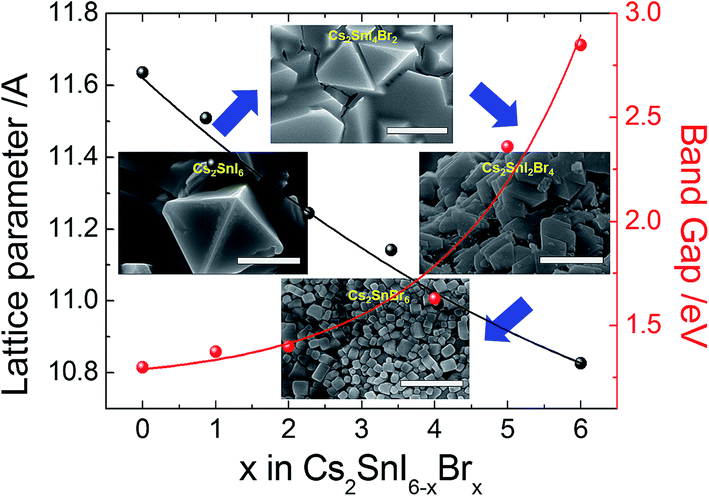 | ||
| Fig. 10 The change in the lattice constant and the shift in the optical band gap both indicate the solid-solution nature of the Cs2SnI6−xBrx system (inset: the surface morphologies of different compounds (note: the scale bar is 1 μm)). | ||
2.3. Device configuration and performance
In our earlier effort we used a standard device fabrication procedure where layers were sequentially deposited on the cathode side of the device. But we soon found that we were having unwanted shorts in the devices coming from the edges for the adjacent layers. In addition, the roughness of the Cs2SnI6 surface layer also contributed to charge recombination in the grain boundaries. In order to improve the device performance, we adopt in this section a different device structure the so-called sandwich structure. In this scheme the two parts (anode and cathode sides) of the device are fabricated separately. Once these steps are done, the two sides are then sandwiched together using a solid state flexible HTM layer as described below. We first describe the performance of a Cs2SnI6 cell using this approach with a blend of different inorganic materials and succinonitrile (Section 3.1), followed by a discussion of cells with Br inclusion in the sensitizer to widen the bandgap (Section 3.2).![[triple bond, length as m-dash]](https://www.rsc.org/images/entities/char_e002.gif) C–(CH2)2–CN) functions as a polymer host medium for ion transport and forms a single plastic poly-crystal at room temperature and because of its high lattice stability it behaves as a solid ion conductor in the presence of Cs2SnI6. Additionally, copper thiocyanate (CuSCN) known as another p-type inorganic material with high hole mobility and compatible band position is also studied.35 The phenomenon of ion transport in our system could not be understood clearly as yet due to the lack of knowledge of the exact structural property correlations. However, macroscopic studies on the basic ionic parameters and their temperature variations provide a wealth of information regarding ion dynamics. The ionic conductivities of solid electrolytes were investigated via AC impedance spectroscopy measurements of symmetric cells with two pieces of platinized FTO glass (cell area: 0.188 cm2, thickness: 20 μm). From well-fitted spectra, one can see a well-defined semicircle at high and intermediate frequencies that is ascribed to the parallel combination of bulk resistance and bulk capacitance, which is a result of the migration of ions and the immobile polymer chains, respectively. The straight line after the semicircle at low frequencies is due to the double layer capacitance formed at the interface between the electrode and electrolyte36,37 (see Fig. 11a). The ionic conductivity of our samples was determined using a Solatron impedance analyzer (SI-1260) with an electrochemical interface (SI-1286) in a wide frequency range between 0.5 Hz and 5.0 MHz at different temperatures. The ionic conductivities σ (S cm−1) of all the samples were then calculated by using the following equation:38
C–(CH2)2–CN) functions as a polymer host medium for ion transport and forms a single plastic poly-crystal at room temperature and because of its high lattice stability it behaves as a solid ion conductor in the presence of Cs2SnI6. Additionally, copper thiocyanate (CuSCN) known as another p-type inorganic material with high hole mobility and compatible band position is also studied.35 The phenomenon of ion transport in our system could not be understood clearly as yet due to the lack of knowledge of the exact structural property correlations. However, macroscopic studies on the basic ionic parameters and their temperature variations provide a wealth of information regarding ion dynamics. The ionic conductivities of solid electrolytes were investigated via AC impedance spectroscopy measurements of symmetric cells with two pieces of platinized FTO glass (cell area: 0.188 cm2, thickness: 20 μm). From well-fitted spectra, one can see a well-defined semicircle at high and intermediate frequencies that is ascribed to the parallel combination of bulk resistance and bulk capacitance, which is a result of the migration of ions and the immobile polymer chains, respectively. The straight line after the semicircle at low frequencies is due to the double layer capacitance formed at the interface between the electrode and electrolyte36,37 (see Fig. 11a). The ionic conductivity of our samples was determined using a Solatron impedance analyzer (SI-1260) with an electrochemical interface (SI-1286) in a wide frequency range between 0.5 Hz and 5.0 MHz at different temperatures. The ionic conductivities σ (S cm−1) of all the samples were then calculated by using the following equation:38where, d is the thickness of the film, and Rb and A are the resistance and cross-sectional area of the film. Rb is obtained from the complex impedance plot at the intersection of the plot and the real impedance axis. From this equation, σ data for electrolytes can be converted from resistance Rb data measured at different temperatures. The equivalent circuit and experimental results at different measuring temperatures are also shown in ESI 4.† On the basis of temperature dependent conductivity studies, we have confirmed the remarkably enhanced ionic conductivity (σ) of a blend of Cs2SnI6 and SN at 25 °C (∼1.04 × 10⁻³ S cm−1) and this was nearly a factor of 1000 higher with respect to that of pure SN (∼3.56 × 10⁻⁷ S cm−1) and CuSCN (at 9.14 × 10⁻⁶ S cm−1) under ambient conditions. Interestingly, the highest conducting value can be obtained by a Cs2SnI6 matrix formed by oxidized CsSnI3 powder with (P1,4)-I (2.45 × 10⁻³ S cm−1).39Fig. 11b bottom shows the temperature dependence of ionic conductivity as a function of 1000/T. The ionic conductivity increases with increasing temperature. The temperature dependence of the conductivity becomes insignificant in the lower temperature range, implying that the contribution of ionic conduction from various pathways may change at different temperatures. The activation energies (Ea) of each sample can be calculated by the Arrhenius type equation:

where σ0 is the pre-exponential factor, and k is the Boltzmann constant. The activation energy, Ea, can be computed from the linear-least-square fit of the data from a log

![[thin space (1/6-em)]](https://www.rsc.org/images/entities/char_2009.gif) σ versus 1/T plot. Activation energy is the energy required for an ion to begin movement. When the ion has acquired sufficient energy, it is able to break away from the donor site and move to another donor site. It can be observed that the ions in highly conducting samples require lower energy for migration.40 In our system, the calculated Ea value for the different samples was decreased in the order Cs2SnI6 > CuSCN > oxidized Cs2SnI6. Interestingly, despite the poor conductivity of the CuSCN matrix system, it shows lower activation energy compared to Cs2SnI6. The lowest Ea value can be found for the oxidized Cs2SnI6. Further improvement can be found by adding (P1,4)-I into Cs2SnI6/SN.39 This blended HTM has a fast ionic conductivity from 5.67 × 10⁻³ S cm−1 at room temperature to 1.95 × 10⁻² S cm−1 at 80 °C. Furthermore, the Cs2SnI6 blended film possesses the ability to form a free-standing and flexible film which can also help improve the mechanical contact (see Fig. 11b inset). In addition, the action of sandwiching the two halves of the device will help improve the contact of the SN/Cs2SnI6 blend with the grain boundaries of the Cs2SnI6 sensitizer, thus improving the device performance. The HOMO position is also determined via UPS (see ESI 5†). It can be seen that the CuSCN has a HOMO level of 5.2 ± 0.12 eV in accordance with the literature.35 In the case of the Cs2SnI6 matrix, a 0.1 eV difference in HOMO values is observed between the starting materials of CsSnI3 and Cs2SnI6. The devices formed by this “sandwich” process are simple and very stable under ambient conditions. This simplicity may make it possible for solar cell manufacturers to eventually replace expensive equipment. The detailed information can be seen in ESI 3.†Fig. 11c shows the XRD pattern of pure SN and the Cs2SnI6/SN films at different temperatures. Even if pure SN does not show the clear peak reported in the literature,41 two peaks at 20° and 28° can be observed. The temperature dependent phase of the Cs2SnI6/SN film was measured using an XRD equipped with a hot stage. The film was heated over the temperature range of 25 °C to 80 °C at the constant heating rate of 5 ° C min−1. The individual diffraction peaks of Cs2SnI6 and SN are clearly observed at room temperature. As the temperature increased, the intensity peak of SN gradually diminished and no diffraction peak was observed at 80 °C (melting temperature). When this heated film was cooled down to room temperature, the peak of SN with the (110) preferred orientation reappeared. This indicated that SN did not have a major effect on the decomposition of Cs2SnI6 to CsI and SnI4, but served as a solid state solvent for supporting the motion of any mobile ions.
σ versus 1/T plot. Activation energy is the energy required for an ion to begin movement. When the ion has acquired sufficient energy, it is able to break away from the donor site and move to another donor site. It can be observed that the ions in highly conducting samples require lower energy for migration.40 In our system, the calculated Ea value for the different samples was decreased in the order Cs2SnI6 > CuSCN > oxidized Cs2SnI6. Interestingly, despite the poor conductivity of the CuSCN matrix system, it shows lower activation energy compared to Cs2SnI6. The lowest Ea value can be found for the oxidized Cs2SnI6. Further improvement can be found by adding (P1,4)-I into Cs2SnI6/SN.39 This blended HTM has a fast ionic conductivity from 5.67 × 10⁻³ S cm−1 at room temperature to 1.95 × 10⁻² S cm−1 at 80 °C. Furthermore, the Cs2SnI6 blended film possesses the ability to form a free-standing and flexible film which can also help improve the mechanical contact (see Fig. 11b inset). In addition, the action of sandwiching the two halves of the device will help improve the contact of the SN/Cs2SnI6 blend with the grain boundaries of the Cs2SnI6 sensitizer, thus improving the device performance. The HOMO position is also determined via UPS (see ESI 5†). It can be seen that the CuSCN has a HOMO level of 5.2 ± 0.12 eV in accordance with the literature.35 In the case of the Cs2SnI6 matrix, a 0.1 eV difference in HOMO values is observed between the starting materials of CsSnI3 and Cs2SnI6. The devices formed by this “sandwich” process are simple and very stable under ambient conditions. This simplicity may make it possible for solar cell manufacturers to eventually replace expensive equipment. The detailed information can be seen in ESI 3.†Fig. 11c shows the XRD pattern of pure SN and the Cs2SnI6/SN films at different temperatures. Even if pure SN does not show the clear peak reported in the literature,41 two peaks at 20° and 28° can be observed. The temperature dependent phase of the Cs2SnI6/SN film was measured using an XRD equipped with a hot stage. The film was heated over the temperature range of 25 °C to 80 °C at the constant heating rate of 5 ° C min−1. The individual diffraction peaks of Cs2SnI6 and SN are clearly observed at room temperature. As the temperature increased, the intensity peak of SN gradually diminished and no diffraction peak was observed at 80 °C (melting temperature). When this heated film was cooled down to room temperature, the peak of SN with the (110) preferred orientation reappeared. This indicated that SN did not have a major effect on the decomposition of Cs2SnI6 to CsI and SnI4, but served as a solid state solvent for supporting the motion of any mobile ions.
 | ||
| Fig. 11 Different solid state ionic conductors as a HTM layer: (a) experimental and fitting impedance spectra at room temperature and (b) Arrhenius plots and photo-images of the different solid state electrolytes. (c) XRD pattern of the Cs2SnI6 mixed in succinonitrile film as a function of temperature (at r.t, 50 °C, 80 °C and cooled to room temperature). | ||
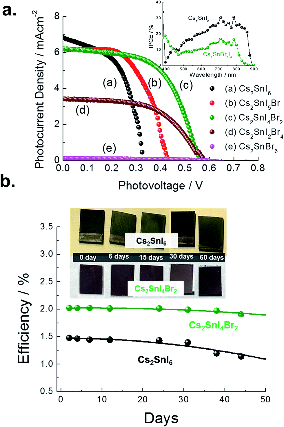 | ||
| Fig. 12 (a) JV characteristic curves of a series of “sandwich” typed cells with different composition of Cs2SnI6−xBrx. The inset shows the IPCE values for Cs2SnI6 (black) and Cs2SnBr2I4 (green). (b) The stability curves for 50 days are shown here for Cs2SnI6 (black), and the Cs2SnBr2I4 (green) based solar cells. | ||
| Reaction | Matched compound | Calculated band gap (eV) | JV characteristics | |||
|---|---|---|---|---|---|---|
| V oc (V) | J sc (mA cm−2) | FF (%) | Eff (%) | |||
| CsI (film) + SnI4 (sol) | Cs2SnI6 | 1.30 | 0.367 | 6.752 | 59.5 | 1.473 |
| CsI:CsBr (7:3, film) + SnI4 (sol) |
Cs2SnI5Br | 1.375 | 0.444 | 6.576 | 55.0 | 1.601 |
| CsI:CsBr (3:7, film) + SnI4 (sol) |
Cs2SnI4Br2 | 1.40 | 0.563 | 6.225 | 57.7 | 2.025 |
| CsBr (film) + SnI4 (sol) | Cs2SnI2Br4 | 1.63 | 0.575 | 3.413 | 54.8 | 1.081 |
| CsI:CsBr (7:3, film) + SnBr4 (sol) |
Cs2SnIBr5 | 2.36 | 0.572 | 0.010 | 37.2 | 0.002 |
| CsBr (film) + SnBr4 (sol) | Cs2SnBr6 | 2.85 | Non | Non | Non | Non |
3 Summary and conclusion
In summary, we have reported in detail our investigation into a two-step solution process to form air-stable molecular semiconducting Cs2SnIxBr6−x iodosalt compounds for potential solar cell applications. There are many challenging processing steps as discussed in the three sections above. However, three major ones stand out: (1) how to form a stoichiometric compound throughout the iodosalt film across the length scale from nanometers to centimeters? We showed in our work that if there is an excess of CsI, in the compound, both electrical and optical performances of the material and the associated device will suffer deterioration. (2) How to form smooth and thick-enough film layers to fabricate a solar device with measurable performance? To achieve this demand, we showed how we had to optimize the CsI crystal structure in Step-1 through optimizing the annealing temperature and duration. In combination with Step-2, we had to optimize the reaction temperature and duration to obtain a thick and stoichiometric Cs2SnIxBr6−x compound. (3) How to choose film layers needed to optimize device performance with appropriate band-alignment without interfacial chemical reactions? As discussed in section 3, we did bandgap alignment engineering and developed a “sandwich” device fabrication process as an example of what can be done in our lab with no special environmental protection.In conclusion, we have demonstrated that our two-step solution processing technique is one of many possible options to synthesize air stable Cs2SnIxBr6−x compounds. We have shown that both the materials and devices fabricated are air-stable, although with low performance, as a start. As with all materials research, to design a higher performance device, an improved starting material is necessary. Based on what we have learned, new synthesis concepts are currently being developed.
4 Experimental section
4.1. Preparation of Cs2SnI6 materials – sequential deposition of Cs2SnI6−xBrx
To coat different thickness Cs2SnI6 layers, a novel two-step coating process (electrospraying technique) has been developed in our laboratory. In the first step, a CsX solution was prepared dissolving 2 g of CsI or CsBr powder (Aldrich, 99.9%) in 1000 mL of a solvent mixture of deionized water and isopropanol (deionized water:isopropanol = 0.1:1 v/v). After sonication for 1 hour, the solutions were loaded into a plastic syringe equipped with a 27-gauge stainless steel needle. The spinning rate was controlled by using a syringe pump (KD Scientific Model 220) at 35–50 μL min−1. An electric field of 12–15 kV was applied between a metal orifice and the ground at a distance of 10 cm by using a power supply (BERTAN SERIES 205B). The CsI solution was directly e-sprayed on TiO2 spheres. The duration of electrospraying controls the thickness of the CsI or CsBr layers and this film was heated in a box furnace (Barnstead/Thermolyne Small Benchtop Muffle Furnaces) at temperatures ranging from 100 °C to 500 °C for 20 min in an ambient atmosphere. In the second step, a solution of Tin(IV) iodide (SnI4) or Tin(IV) bromide (SnBr4) in ethanol (0.1 g mL−1) was then introduced into the CsI or CsBr layer by drop coating. The drop process was repeated several times until the color of the covered CsI and CsBr layers changed from black to light yellow. This film was heated in air at 110 °C for 20 min.
4.2. Preparation for device fabrication
Unless stated otherwise, all manipulations described below were performed in air under ambient laboratory conditions.On the prepared dense TiO2 blocking layer, the dispersed Sn–TiO2 solution was electrosprayed directly onto the conducting substrates. To prepare the hierarchically structured TiO2 sphere, an electric field of 12 kV was applied between the metal orifice and the conducting substrate. The feed rate was controlled by using a syringe pump at 40–45 μL min−1. In order to form a uniform thickness in a large area, the nozzle and the substrate were placed on a motion control system with a microprocessor. The TiO2 films were annealed at 500 °C for 45 min. As a next step, TiCl4 aqueous solution has been applied to the E-sprayed TiO2 film. An aqueous stock solution of 2 M TiCl4 was diluted to 0.02 M in deionized water and the sintered electrodes were immersed into this solution and stored in an oven at 70 °C for 20 min in a closed vessel. After flushing with deionized water and drying, the electrodes were gradually sintered again at 150 °C for 15 min, at 320 °C for 10 min, and at 500 °C for 30 min.
4.3. Characterization
Powder and film X-ray diffraction patterns were collected in-house using a Rigaku MiniFlex 600 X-ray diffractometer (Cu Kα, 1.5406 Å) operating at 40 kV and 15 mA. Synchrotron radiation (APS, 11BM-B) was used for selected annealing temperatures of Cs2SnI6 to identify the decomposition temperature of the compounds. The obtained data were analyzed using the JANA2006 software package.44 Optical diffuse-reflectance spectra were collected at room temperature using a Shimadzu UV-3600 PC double-beam, double-monochromator spectrophotometer for powdered samples using BaSO4 as a 100% reflectance reference. XPS measurements were obtained using a monochromatic Al Kα source at hν = 1486 cm−1. A typical operating pressure for XPS and UPS measurements was 1 × 10⁻⁸ Torr. XPS spectra were collected at a pass energy of 20.0 eV and a dwell time of 10 ms. An electron flood gun was used to eliminate charging effects. All binding energies were referenced to an adventitious C(1 s) energy of 285.0 eV. UPS spectra were collected with a 21.2 eV He(1) source with a pass energy of 2.0 eV and a step size of 0.01 eV. A sample bias of −10 V was applied to determine the secondary electron cutoff value via curve fitting.A Newport-Oriel® IQE-200 ACDC was used to measure incident photon to charge carrier efficiency (IPCE). The devices were evaluated under 100 mW cm−2 AM 1.5G simulated sunlight with a class A solar cell analyzer (Spectra Nova Tech.). A silicon solar cell fitted with a KG3 filter tested and certified by the National Renewable Energy Laboratory (NREL) was used for calibration. The KG3 filter accounts for the different light absorption between the perovskite based solar cell and the silicon solar cell, and it ensures that the spectral mismatch correction factor approaches unity.
Acknowledgements
This research was supported as part of the Argonne-Northwestern Solar Energy Research Center (ANSER), an Energy Frontier Research Center funded by the U.S. Department of Energy, Office of Science, Office of Basic Energy Sciences (award no. DE-SC0001059), and Institute for Sustainability and Energy at Northwestern (ISEN). We thank the NSF-MRSEC program through the Northwestern University Materials Research Science and Engineering Center for characterization facilities (DMR-1121262). XRD measurements were performed at the J. B. Cohen X-Ray Diffraction Facility, supported by the MRSEC program of the National Science Foundation (DMR-1121262) at the Materials Research Center of Northwestern University. Electron microscopy and elemental analysis were carried out at the Electron Probe Instrumentation Center (EPIC) at Northwestern University. The use of the Advanced Photon Source was supported by the US Department of Energy, Office of Science, Office of Basic Energy Sciences, under contract No. DE-AC02-06CH11357. We thank M. G. Kanatzidis and C. C. Stoumpos for discussions and their suggestions.References
- M. M. Lee, J. Teuscher, T. Miyasaka, T. N. Murakami and H. J. Snaith, Efficient Hybrid Solar Cells Based on Meso-Superstructured Organometal Halide Perovskites, Science, 2012, 338(6107), 643–647 CrossRef CAS PubMed.
- J. Burschka, N. Pellet, S.-J. Moon, R. Humphry-Baker, P. Gao, M. K. Nazeeruddin and M. Gratzel, Sequential deposition as a route to high-performance perovskite-sensitized solar cells, Nature, 2013, 499(7458), 316–319 CrossRef CAS PubMed.
- M. Liu, M. B. Johnston and H. J. Snaith, Efficient planar heterojunction perovskite solar cells by vapour deposition, Nature, 2013, 501(7467), 395–398 CrossRef CAS PubMed.
- J. H. Noh, S. H. Im, J. H. Heo, T. N. Mandal and S. I. Seok, Chemical Management for Colorful, Efficient, and Stable Inorganic–Organic Hybrid Nanostructured Solar Cells, Nano Lett., 2013, 13(4), 1764–1769 CrossRef CAS PubMed.
- Y. Ogomi, A. Morita, S. Tsukamoto, T. Saitho, N. Fujikawa, Q. Shen, T. Toyoda, K. Yoshino, S. S. Pandey, T. Ma and S. Hayase, CH3NH3SnxPb(1−x)I3 Perovskite Solar Cells Covering up to 1060 nm, J. Phys. Chem. Lett., 2014, 5(6), 1004–1011 CrossRef CAS PubMed.
- F. Hao, C. C. Stoumpos, R. P. H. Chang and M. G. Kanatzidis, Anomalous Band Gap Behavior in Mixed Sn and Pb Perovskites Enables Broadening of Absorption Spectrum in Solar Cells, J. Am. Chem. Soc., 2014, 136(22), 8094–8099 CrossRef CAS PubMed.
- H.-S. Kim, C.-R. Lee, J.-H. Im, K.-B. Lee, T. Moehl, A. Marchioro, S.-J. Moon, R. Humphry-Baker, J.-H. Yum, J. E. Moser, M. Grätzel and N.-G. Park, Lead Iodide Perovskite Sensitized All-Solid-State Submicron Thin Film Mesoscopic Solar Cell with Efficiency Exceeding 9%, Sci. Rep., 2012, 2, 591 Search PubMed.
- G. E. Eperon, S. D. Stranks, C. Menelaou, M. B. Johnston, L. M. Herz and H. J. Snaith, Formamidinium lead trihalide: a broadly tunable perovskite for efficient planar heterojunction solar cells, Energy Environ. Sci., 2014, 7(3), 982–988 CAS.
- T. M. Koh, K. Fu, Y. Fang, S. Chen, T. C. Sum, N. Mathews, S. G. Mhaisalkar, P. P. Boix and T. Baikie, Formamidinium-Containing Metal-Halide: An Alternative Material for Near-IR Absorption Perovskite Solar Cells, J. Phys. Chem. C, 2014, 118(30), 16458–16462 CAS.
- G. E. Eperon, G. M. Paterno, R. J. Sutton, A. Zampetti, A. A. Haghighirad, F. Cacialli and H. J. Snaith, Inorganic caesium lead iodide perovskite solar cells, J. Mater. Chem. A, 2015, 3(39), 19688–19695 CAS.
- I. C. Smith, E. T. Hoke, D. Solis-Ibarra, M. D. McGehee and H. I. Karunadasa, A Layered Hybrid Perovskite Solar-Cell Absorber with Enhanced Moisture Stability, Angew. Chem., 2014, 126(42), 11414–11417 CrossRef.
- G. Niu, W. Li, F. Meng, L. Wang, H. Dong and Y. Qiu, Study on the stability of CH3NH3PbI3 films and the effect of post-modification by aluminum oxide in all-solid-state hybrid solar cells, J. Mater. Chem. A, 2014, 2(3), 705–710 CAS.
- M. A. Green, A. Ho-Baillie and H. J. Snaith, The emergence of perovskite solar cells, Nat. Photonics, 2014, 8(7), 506–514 CrossRef CAS.
- B. Lee, C. C. Stoumpos, N. Zhou, F. Hao, C. Malliakas, C.-Y. Yeh, T. J. Marks, M. G. Kanatzidis and R. P. H. Chang, Air-Stable Molecular Semiconducting Iodosalts for Solar Cell Applications: Cs2SnI6 as a Hole Conductor, J. Am. Chem. Soc., 2014, 136(43), 15379–15385 CrossRef CAS PubMed.
- C. C. Stoumpos, C. D. Malliakas and M. G. Kanatzidis, Semiconducting Tin and Lead Iodide Perovskites with Organic Cations: Phase Transitions, High Mobilities, and Near-Infrared Photoluminescent Properties, Inorg. Chem., 2013, 52(15), 9019–9038 CrossRef CAS PubMed.
- Z. Xiao, H. Lei, X. Zhang, Y. Zhou, H. Hosono and T. Kamiya, Ligand-Hole in [SnI6] Unit and Origin of Band Gap in Photovoltaic Perovskite Variant Cs2SnI6, Bull. Chem. Soc. Jpn., 2015, 88(9), 1250–1255 CrossRef CAS.
- G. E. Eperon, V. M. Burlakov, P. Docampo, A. Goriely and H. J. Snaith, Morphological Control for High Performance, Solution-Processed Planar Heterojunction Perovskite Solar Cells, Adv. Funct. Mater., 2014, 24(1), 151–157 CrossRef CAS.
- B. Saparov, J.-P. Sun, W. Meng, Z. Xiao, H.-S. Duan, O. Gunawan, D. Shin, I. G. Hill, Y. Yan and D. B. Mitzi, Thin-Film Deposition and Characterization of a Sn-Deficient Perovskite Derivative Cs2SnI6, Chem. Mater., 2016, 28(7), 2315–2322 CrossRef CAS.
- A. E. Maughan, A. M. Ganose, M. M. Bordelon, E. M. Miller, D. O. Scanlon and J. R. Neilson, Defect Tolerance to Intolerance in the Vacancy-Ordered Double Perovskite Semiconductors Cs2SnI6 and Cs2TeI6, J. Am. Chem. Soc., 2016, 138(27), 8453–8464 CrossRef CAS PubMed.
- Z. Xiao, Y. Zhou, H. Hosono and T. Kamiya, Intrinsic defects in a photovoltaic perovskite variant Cs2SnI6, Phys. Chem. Chem. Phys., 2015, 17(29), 18900–18903 RSC.
- D. R. Stull, Vapor Pressure of Pure Substances. Organic and Inorganic Compounds, Ind. Eng. Chem., 1947, 39(4), 517–540 CrossRef CAS.
- W. Shockley and H. J. Queisser, Detailed Balance Limit of Efficiency of p–n Junction Solar Cells, J. Appl. Phys., 1961, 32(3), 510–519 CrossRef CAS.
- H. Lin, C. P. Huang, W. Li, C. Ni, S. I. Shah and Y.-H. Tseng, Size dependency of nanocrystalline TiO2 on its optical property and photocatalytic reactivity exemplified by 2-chlorophenol, Appl. Catal., B, 2006, 68(1–2), 1–11 CrossRef CAS.
- Y. Ling, G. Wang, D. A. Wheeler, J. Z. Zhang and Y. Li, Sn-Doped Hematite Nanostructures for Photoelectrochemical Water Splitting, Nano Lett., 2011, 11(5), 2119–2125 CrossRef CAS PubMed.
- T. Hirata, K. Ishioka, M. Kitajima and H. Doi, Concentration dependence of optical phonons in the TiO2–SnO2 system, Phys. Rev. B: Condens. Matter Mater. Phys., 1996, 53(13), 8442–8448 CrossRef CAS.
- P. V. Kamat, Photochemistry on nonreactive and reactive (semiconductor) surfaces, Chem. Rev., 1993, 93(1), 267–300 CrossRef CAS.
- S. Gubbala, V. Chakrapani, V. Kumar and M. K. Sunkara, Band-Edge Engineered Hybrid Structures for Dye-Sensitized Solar Cells Based on SnO2 Nanowires, Adv. Funct. Mater., 2008, 18(16), 2411–2418 CrossRef CAS.
- D. Sabba, H. K. Mulmudi, R. R. Prabhakar, T. Krishnamoorthy, T. Baikie, P. P. Boix, S. Mhaisalkar and N. Mathews, Impact of Anionic Br-Substitution on Open Circuit Voltage in Lead Free Perovskite (CsSnI3−xBrx) Solar Cells, J. Phys. Chem. C, 2015, 119(4), 1763–1767 CAS.
- A. Kaltzoglou, M. Antoniadou, A. G. Kontos, C. C. Stoumpos, D. Perganti, E. Siranidi, V. Raptis, K. Trohidou, V. Psycharis, M. G. Kanatzidis and P. Falaras, Optical-Vibrational Properties of the Cs2SnX6 (X = Cl, Br, I) Defect Perovskites and Hole-Transport Efficiency in Dye-Sensitized Solar Cells, J. Phys. Chem. C, 2016, 120(22), 11777–11785 CAS.
- C. Li, J. Wei, M. Sato, H. Koike, Z.-Z. Xie, Y.-Q. Li, K. Kanai, S. Kera, N. Ueno and J.-X. Tang, Halide-Substituted Electronic Properties of Organometal Halide Perovskite Films: Direct and Inverse Photoemission Studies, ACS Appl. Mater. Interfaces, 2016, 8(18), 11526–11531 CAS.
- L. Schmidt-Mende, S. M. Zakeeruddin and M. Grätzel, Efficiency improvement in solid-state-dye-sensitized photovoltaics with an amphiphilic ruthenium-dye, Appl. Phys. Lett., 2005, 86(1), 013504 CrossRef.
- P. Wang, Q. Dai, S. M. Zakeeruddin, M. Forsyth, D. R. MacFarlane and M. Grätzel, Ambient Temperature Plastic Crystal Electrolyte for Efficient, All-Solid-State Dye-Sensitized Solar Cell, J. Am. Chem. Soc., 2004, 126(42), 13590–13591 CrossRef CAS PubMed.
- D. R. MacFarlane and M. Forsyth, Plastic Crystal Electrolyte Materials: New Perspectives on Solid State Ionics, Adv. Mater., 2001, 13(12–13), 957–966 CrossRef CAS.
- I. Chung, B. Lee, J. He, R. P. H. Chang and M. G. Kanatzidis, All-solid-state dye-sensitized solar cells with high efficiency, Nature, 2012, 485(7399), 486–489 CrossRef CAS PubMed.
- P. Qin, S. Tanaka, S. Ito, N. Tetreault, K. Manabe, H. Nishino, M. K. Nazeeruddin and M. Grätzel, Inorganic hole conductor-based lead halide perovskite solar cells with 12.4% conversion efficiency, Nat. Commun., 2014, 5, 3834 CAS.
- X. Qian, N. Gu, Z. Cheng, X. Yang, E. Wang and S. Dong, Impedance study of (PEO)10LiClO4–Al2O3 composite polymer electrolyte with blocking electrodes, Electrochim. Acta, 2001, 46(12), 1829–1836 CrossRef CAS.
- W. Liu, N. Liu, J. Sun, P.-C. Hsu, Y. Li, H.-W. Lee and Y. Cui, Ionic Conductivity Enhancement of Polymer Electrolytes with Ceramic Nanowire Fillers, Nano Lett., 2015, 15(4), 2740–2745 CrossRef CAS PubMed.
- C. Meng, C. Liu, L. Chen, C. Hu and S. Fan, Highly Flexible and All-Solid-State Paper like Polymer Supercapacitors, Nano Lett., 2010, 10(10), 4025–4031 CrossRef CAS PubMed.
- B. Lee, D. B. Buchholz, P. Guo, D.-K. Hwang and R. P. H. Chang, Optimizing the Performance of a Plastic Dye-Sensitized Solar Cell, J. Phys. Chem. C, 2011, 115(19), 9787–9796 CAS.
- M. H. Buraidah, L. P. Teo, S. R. Majid and A. K. Arof, Ionic conductivity by correlated barrier hopping in NH4I doped chitosan solid electrolyte, Phys. B, 2009, 404(8–11), 1373–1379 CrossRef CAS.
- M. Echeverri, N. Kim and T. Kyu, Ionic Conductivity in Relation to Ternary Phase Diagram of Poly(ethylene oxide), Succinonitrile, and Lithium Bis(trifluoromethane)sulfonimide Blends, Macromolecules, 2012, 45(15), 6068–6077 CrossRef CAS.
- B. Lee, D. B. Buchholz and R. P. H. Chang, An all carbon counter electrode for dye sensitized solar cells, Energy Environ. Sci., 2012, 5(5), 6941–6952 CAS.
- I. Chung, J.-H. Song, J. Im, J. Androulakis, C. D. Malliakas, H. Li, A. J. Freeman, J. T. Kenney and M. G. Kanatzidis, CsSnI3: Semiconductor or Metal? High Electrical Conductivity and Strong Near-Infrared Photoluminescence from a Single Material. High Hole Mobility and Phase-Transitions, J. Am. Chem. Soc., 2012, 134(20), 8579–8587 CrossRef CAS PubMed.
- V. Petříček, M. Dušek and L. Palatinus, Crystallographic Computing System JANA2006: General features, in Zeitschrift für Kristallographie – Crystalline Materials, 2014, vol. 229, p. 345 Search PubMed.
Footnote |
| † Electronic supplementary information (ESI) available: Additional SEM images, profilometry data and transmission spectra of the CsX films. See DOI: 10.1039/c7se00100b |
| This journal is © The Royal Society of Chemistry 2017 |