
Effect of anodization time on photovoltaic properties of nanoporous silicon based solar cells†
Hamid Ghorbani
Shiraz
 ab
ab
aSchool of Chemical Engineering, College of Engineering, University of Tehran, Tehran, Iran. E-mail: Ghorbani_Shiraz@ut.ac.ir
bYoung Researchers and Elite Club, Mashhad Branch, Islamic Azad University, Mashhad, Iran
First published on 20th March 2017
Abstract
This study describes the fabrication procedure of hybrid porous silicon-based solar cells. Porous silicon was synthesized by electrochemical anodization (EA) of polysilicon under an etching time of 6, 8, and 10 min, using HF/EtOH solution. The fabricated template was employed as an active substrate to undertake an n-type semiconductor. TiO2 nanoparticles (NPs), as emitter, were immobilized over the porous substrate using an electrophoretic deposition (EPD) method. Indium-tin oxide (ITO), as the front electrode, was sputtered to extract the carriers using a DC magnetron sputtering technique. The surface morphology was studied by observing the FESEM images. Optical properties of the proposed system were investigated by reflection and absorption spectra. Finally, photovoltaic measurements of the fabricated cells were studied for different samples. The measurements were accomplished under AM 1.5 illumination using a solar simulator. It was demonstrated that the 6 min anodized sample showed the highest performance; the efficiency was 1.57 and 2.73 times higher than that of the 8 and 10 min samples, respectively. The preferential 6 min sample showed lowest reflection as well as a more appropriate band gap. The competitive efficiency could be attributed to the coherent and compact p–n junctions as well as to the qualified immobilization of the hole-barrier layer (metal oxide).
1. Introduction
Over last few decades, silicon and titanium have been employed in a wide range of applications, owing to their unique optical and electrical features.1,2 Among them, high performance solar cells are recognized as efficient optoelectronic devices.3 There are several barriers in the field of fabrication of crystalline silicon (c-Si) solar cells, such as introduction of impurity in the semiconductors through an ion diffusion process. Therefore, studies that focus on the facility of this operation could play a great role with respect to the fabrication of efficient solar cells. In addition, high availability of light radiation is a great criterion for solar cell performance.4 In this regard, solar cell architectures have been modified using silicon structures to increase the light assessment over cells. According to the literature, porous silicon (PS) as an anti-reflection coating (ARC) has been employed widely as a decoration in solar cells.5,6 Moreover, PS could be employed as a light trapping structure due to its surface roughness.7 This effect offers a high degree of anti-reflection property and obviates ARC polishing step during manufacturing; thereby, the fabrication cost can be reduced.8The porous silicon structure has been studied theoretically and practically as an ARC. In this regard, Urteaga et al.9 developed numerical simulations to optimize the performance of multilayer porous silicon by maximizing the energy transference and minimizing the weighted reflectance. They showed that three layers structure could result in an energy loss of 4.2%, which is approximately 50% lower than conventional silicon solar cells. Tang et al.10 employed trenched electrodes to enhance the efficiency of polycrystalline silicon solar cells through nanoporous silicon layer. Cells with trenched electrode-contacts obtained a higher short-circuit current and conversion efficiency, compared to planar electrode contacts. Recently, Gangadevi et al.11 proposed a dye-sensitized solar cell including the PS nanostructure as a template for sensitizers. They examined various etching times to find the optimized substrate.
Generally, porous silicon has great potential in optoelectronic devices, particularly solar cells. As a potential research, porous silicon can be used in the main architecture of silicon solar cells.
In this study, EA was used as a very simple technique to fabricate PS as a substrate for the emitter layer. This structure could provide a broad surface area12 for the immobilization of n-type semiconductors. Porous (base) thickness is a significant parameter in this structure and the quality of the etching process is a decisive factor in regard to the solar cell performance. Therefore, the effects of the anodization duration (AD) on the main features of the fabricated solar cells are discussed.
2. Experimental and characterization
The PS substrates were provided using the procedure described elsewhere13 with the exception of a p-type polycrystalline Si wafer. However, the etching process was carried out under direct current and an anodization duration of 6, 8, and 10 minutes: AD-6, AD-8, and AD-10. After the anodization process, each sample was rinsed with DI water and dried. EPD was carried out using platinum (Pt) as the counter electrode14 for the deposition of TiO2 NPs over the porous substrate. TiO2 NPs (P25-Degussa) was dispersed in a mixture of acetone (trace) and iso-propyl alcohol; then, it was ultra-sonicated for 1 h. During EPD, an electric field was applied between PS and Pt at a distance of 2 cm in the colloidal solution using constant potential in the order of 100 V. After the process, the samples were heated to 100 °C in vacuum to ensure better immobilization. Finally, the samples were processed by indium-tin oxide (ITO) sputtering (MSS 160, ACECR). FESEM (Mira 3-XMU) images were employed to study the morphology and surface characterization of the samples (PS/TiO2/ITO). The reflection spectra were measured using a (Avanspec 2048) spectrophotometer. In addition, the photovoltaic measurements were carried out using a solar simulator (Luzchem) under AM 1.5 conditions. The EQE spectra were characterized using an EQE system (Enlitech, Taiwan). The photoluminescence spectra (PL) were measured using a Varian Cary Eclipse Fluorescence Spectrophotometer. Before measurements, the instrument was calibrated using a reference silicon solar cell.3. Results and discussions
Since the TiO2 NPs are immobilized as an emitter (n-type) layer, the control of EPD process (to ensure the deposition of a given threshold for emitter, <1 μm) is considerable in this regard. Clearly, the EPD media is a decisive factor toward the quality of immobilized layer, such as thickness. It has been demonstrated that the thin film deposition of TiO2 could occur when iso-propyl alcohol is employed as the EPD electrolyte. Dor et al.15 showed that thin film of TiO2 could be produced by EPD with a well-controlled thickness. They examined iso-propyl alcohol, ethanol, and methanol as an EPD electrolyte. They reported that iso-propyl alcohol could define the lowest thickness of deposited film, compared to the others. In fact, the difference in the dielectric constant of the solvents determines the rate of the deposition process through the ratio of the charged particles and the free ions in the media. In addition, it was recognized that, regardless of the type of solvent, the density of the deposited film decreases with increasing film thickness. Consequently, iso-propyl could offer a thin and dense film.In this study, iso-propyl alcohol was used as an EPD media; therefore, the requirement of emitter layer (thickness) could be met, as far as possible. Moreover, the dense (and compact) layer is deposited; hence, the structural defects may be quenched as far as possible.
On the other hand, due to the low mobility of the minor carrier within the porous media, control of the porous thickness is significant.7 Therefore, optimization of porous thickness through variation in AD could result in efficient performance.
The FESEM images demonstrate the effect of AD on the morphology of PS (Fig. 1). As illustrated, the planar etching process resulted in uniform surface patterns. The pore and crack edges for AD-6 are distinguished through their sharpness as well as shining regions. The grain boundaries are most favorable etching centers, and a heavy process occurs at these points. This phenomenon results in sharp-tipped sidewalls located far from the grain boundaries. In the case of longer AD, however, the abrasion of sharp-tips (during intense etching) results in chamfer edges; which is recognized in AD-8 and AD-10. In addition, the shining regions originate from the structural component; i.e., the shine points operate as potential sites for TiO2 immobilization (ESI (S1)†).
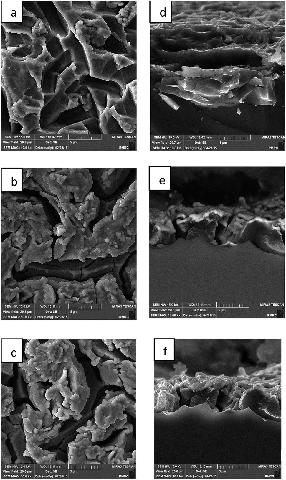 | ||
| Fig. 1 Top-view FESEM images for PS anodized for (a) 6 min, (b) 8 min, and (c) 10 min porous sample; cross-view FESEM images of sample anodized for (d) 6 min, (e) 8 min, and (f) 10 min. | ||
Fig. 1 shows the cross view of the proposed samples (AD-6, AD-8, and AD-10 in Fig. 1d–f, respectively). The average thickness in the samples of AD-6, AD-8, and AD-10 min are 2.5–3, 4, and 4.5 μm, respectively.
TiO2 in the AD-6 is immobilized and the interface of the deposited TiO2 (white shell) and the underlying layer cannot be recognized. The TiO2 NPs diffuse within the porous media and fill the pores. This phenomenon leads to the integration and distribution of p–n junctions. In the case of AD-8 and AD-10, the deposited layer could be clearly defined with an average thickness of 500 nm. The measurements ensure that the bathetic points cannot prepare potential sites for the accommodation of titanium NPs. This comes from the nature of EPD technique; it defines the tips as more appropriate sites for immobilizations due to higher charge density. The even structures and the porous floor cannot underlie the EPD process (S2†). The latter approaches (AD-8 and AD-10) have a detrimental effect on cell performance by avoiding the fabrication of local p–n junctions on the floor with pores and cracks. The sputtered layer of ITO could be (particularly) recognized from the shiny points in the images. However, the cross-view images show that the sputtered ITO has diffused in the beneath structure. This approach supplies the extraction agents close to p–n junctions. Hence, the collection of photogenerated carriers could improve. Therefore, it seems that they are less likely to recombine.
Clearly, FESEM shows that the surface morphology is not a sensitive function of time because the etching mechanism does not change considerably over the surface.16
As described (S3†), the heterojunction solar cell was fabricated based on silicon and TiO2 NPs, which were employed as the base and emitter, respectively. Moreover, the sputtered ITO layer was devised as the front electrode. In addition, the new architecture solar cell benefits from PS as broad scaffold for deposition of TiO2 NPs, ARC, and light trapping array.
It is noticeable that, TiO2 is employed as an anti-reflection layer in conventional c-Si solar cell. In addition, PS is also a strong anti-reflection layer. Therefore, the proposed solar cell possesses a strong ARC property through synergic effect.
Fig. 2 shows the reflective spectrum of the bare Si-substrate and treated samples. AM 1.5 G solar spectrum is also illustrated in Fig. 2 for comparison.
 | ||
| Fig. 2 Reflective spectrum of the Si-substrate and porous samples in presence of AM 1.5. | ||
Compared to the bare Si-substrate,22 the reflective spectra for the porous samples demonstrate the potential anti-reflection property; the treated samples show low reflection in the range of 300–900 nm. The lowest reflectance of less than 3% was achieved for AD-6/TiO2/ITO. As AD decreases, a blue-shift at a low reflection could be observed. In comparison to bare silicon, all the examined samples resulted in better performance as ARC. The AD-6/TiO2/ITO is a good choice for use in optoelectronic devices particularly solar cell applications; it is defined due to the low reflection range almost matching the high radiated-energy band of the AM 1.5 solar spectrum. Absorption is one of the key factors toward efficient solar cells. In this regard, all the samples were studied by measuring the optical absorption spectra in the wavelength range 300–900 nm using a UV-Vis spectrophotometer. The optical absorption data were analyzed using the Tauc equation for crystal structure:17
| (αhν)2 = k(hν − Eg) | (1) |
Fig. S4† shows the J–V characterizations (as well as external quantum efficiency (EQE)) for competitive samples, AD-6/TiO2/ITO, AD-8/TiO2/ITO, and AD-10/TiO2/ITO. The photovoltaic parameters for all samples (with and without TiO2) are listed in Table 1.
| Item | J SC (mA cm−2) | V OC (mV) | FF (%) | η |
|---|---|---|---|---|
| AD-6/TiO2/ITO | 22 | 427 | 56 | 5.2 |
| AD-8/TiO2/ITO | 19 | 382 | 46 | 3.3 |
| AD-10/TiO2/ITO | 17 | 323 | 36 | 1.9 |
| AD-6/ITO | 8 | 211 | 17 | 0.2 |
| AD-8/ITO | 6 | 150 | 15 | 0.1 |
| AD-10/ITO | 3 | 79 | 10 | 0.02 |
Clearly, the trivial performance of the devices proposed without TiO2 could be attributed to the lack of hole-barrier layer; i.e., despite the presence of transparent conductive oxide layer the created electrons and holes (that may be produced in the interface of PS/ITO) are quickly recombined. The fast recombination is attributed to the numerous defects in the PS. That is why their FFs are very low, compared to the TiO2 equipped devices.
It is possible that the poor junction between n-type semiconductor and p-type PS substrate leads to relatively high series resistance in the device, particularly for higher duration of the process. Technically, as porous thickness decreases, the efficiency of the proposed solar cell increases. Because the lower AD samples lead to compact junction, a better quality of the p–n junction is expected. In fact, this approach integrates the PS media (and interface of PS/TiO2) and modifies the states that can act as recombination centers or can cause diffraction on electron pathway. In addition, FF depends on the series resistance (Rs), which originates particularly from the charge transport properties20 and internal defects and recombination rate.21 Further discussions are extended in S4.† Conclusively, the enhancement of the porous thickness raises the recombination rate and has a detrimental effect on the photovoltaic performance.
Table 1 may initially convey that anodization has a detrimental effect on the performance of the proposed solar cell. Generally, the statement cannot be supported. According to the literature17 a 10 min anodization time may offer a transitional condition with regard to the performance. Experimentally, it was proven that for an anodization time that exceeds 10 min, a significant decrease in the photovoltaic parameters can occur. This may be due to the heavy and intense etching process and porous structure; in fact, they are a decisive factor with regard to the carrier transfer model at the interface of PS/TiO2 (junction).23 Therefore, the high series resistance and low VOC and JSC can be obtained. With this in mind, we consider the lower anodization time. The measurement shows that as the AD decreases, the photovoltaic parameters increase. In comparison, the improvement of parameters is exponential for AD-8 and AD-6. Apart from that, the surface reflection and band gap widening data could be considered. The preliminary modelling based on the data, demonstrated that considerable absorption and less than 0.5% reflection for an anodization time of ∼5 min (ref. 17) could be achieved. In addition, the band gap exceeds that of 6 min, which in turn assists the formation of electron–hole pairs.
Overall, the key role of porous silicon with respect to the introduction of an uneven substrate (consequently, uneven surface of TiO2 immobilized layer) should not be ignored. This improves the optical properties, such as antireflection, light trapping, photoluminescence,9,11 and band gap broadening. Moreover, the porous substrate broadens the surface area for deposition of TiO2 NPs; hence, it extends the junction area. In addition, PS could play a great role in the diode behaviour of the proposed device due to the improvement of the rectifying behaviour of PS, as has been demonstrated.13 However, for the anodization time far from the optimized value (anodization time ∼5 min), the EA has a destructive effect on the architecture and may partially cover the abovementioned advantages.
Herein, a brief discussion on the heterojunction of TiO2/PS (n/p junction) is considered. This heterojunction could play a key role in regard to the blockage of minority carriers due to recombination. In fact, the rate of recombination decreases significantly in the junction compared to the architecture without TiO2. The VOC and JSC for TiO2/PS could be considerable; this phenomenon was ascribed to the process occurring at the interface. It was demonstrated that for a fixed voltage, the presence of hole-blockage layer could reduce the lower dark current considerably; consequently, a higher VOC could be recognized. On the other hand, JSC for cells equipped with TiO2 could be related to the number of extracted carriers. It was recognized that the TiO2 NPs have great potential for reducing hole recombination. The presence of a TiO2 layer (hole-barrier layer) could improve the JSC. However, this property could not be found in the solely PS system (p-type).11,16 In addition, the concept of lifetime could be considerable in this regard. The lifetime of hole has a linear correlation with the reciprocal of the recombination velocity happened in the TiO2/PS interface. It was proven that the hybrid junction consists of several Si–O–Ti functions that could significantly reduce the recombination velocity.24
Fig. 3 presents the histogram of the PCE values for 16 competitive samples. The efficiencies obtained were relatively low compared to the typically polysilicon-based solar cells.
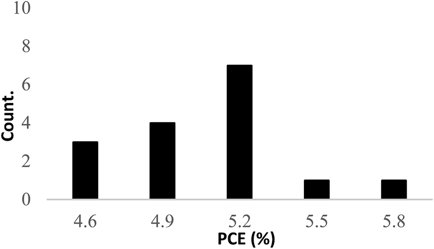 | ||
| Fig. 3 Histogram of the PCE for 16 examined solar cell. | ||
The low performance of this new architecture may be due to a structural deficiency:25 the crystallography defects within the silicon wafer, etched sharp edges, and dangling bands.
We studied the proposed system from the viewpoint of the energy band diagram, which showed promising results. Generally, TiO2 is n-type semiconductor and its band gap is estimated to be ∼3.2 eV.26 In contrast, PS is p-type semiconductor with a given band gap of Eg eV. Thus, a heterojunction is formed between TiO2 and PS, as TiO2 is immobilized over PS. Fig. 4 shows the typical energy band structure for the resulting heterojunction. We examined the rectification of silicon/titanium that had been prepared by the same procedure. The rectification measurements showed very poor results. This approach was attributed to the position of the silicon and titanium band structure. It was proven that the etching process broadens the silicon band gap,27i.e., the Eg increases. Therefore, the anodization process improves the rectification mode. The band structures in our proposed architecture would be arranged, as illustrated in Fig. 4. Generally, the offset of valence bands (ΔEV) and conduction bands (ΔEC) for the proposed structure are so that there would be a barrier that prevents the flowing of holes from PS to TiO2; this alignment allows the electrons to flow from silicon to TiO2.
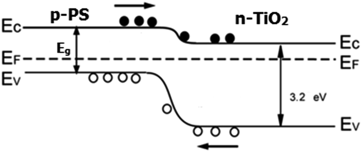 | ||
| Fig. 4 Energy band structure for the proposed heterojunction solar cell. | ||
The PL peak demonstrates that the non-radiative recombination is negligible. The widening of the peaks translates the coupling of phonon within the TiO2 NPs layer.17
To investigate the junction interface on the solar cells performance, we considered the PL spectra for fabricated samples (Fig. S5†). According to Fig. S5,† AD-6 offers strong PL quenching compared to the others. The higher quenching could be attributed to efficient charge transfer at the junction interface; i.e., the interface between the silicon substrate and metal oxide layer demonstrates an efficient charge separation/transfer process. In fact, since the charge transfer resistance at the interface of TiO2/PS has abated, the PL response was considerable. The similarity of the PL pattern asserts that the mechanism of charge transfer could not be influenced by the PS substrate17 and is similar for all the samples. However, the similarity is important in the case of the rate of carrier mobility.
4. Conclusion
In summary, PS was fabricated, using a p-type polysilicon wafer through the EA process and used as a substrate for the immobilization of n-type semiconductor (TiO2 NPs). The porous thickness and cell efficiency depends strongly on the etching duration, while their morphology does not change abruptly with reaction time. Carrier extraction plays an important role in this regard; a lower anodization time results in a thin porous structure, which leads to optimal extraction. Overall, AD-6 offers higher performance by a factor of 1.44 and 2.25 rather than AD-8 and AD-10, respectively. Furthermore, in the case of PS, the band gap width is much wider than that of bulk silicon. This widening of the band energy could boost the performance of PS-based photovoltaic cells. The PS ARC property is another advantage that should not be ignored. In addition, the presence of TiO2 crystals has a synergic effect on the ARC. The lowest reflectance of <3% was achieved, highlighting its potential as an ARC structure.Notes and references
- H. G. Shiraz, F. R. Astaraei, S. Fardindoost and Z. S. Hosseini, Decorated CNT based on porous silicon for hydrogen gas sensing at room temperature, RSC Adv., 2016, 6, 44410–44414 RSC.
- H. G. Shiraz and R. Seyfollahi, Hybrid system for potential room temperature hydrogen storage, Vacuum, 2016, 131, 115–119 CrossRef CAS.
- X. Shen, Z. Xia, L. Chen, S. Li and J. Zhao, Optical and electrical enhancement for high performance hybrid Si/organic heterojunction solar cells using gold nanoparticles, Electrochim. Acta, 2016, 222, 1387–1392 CrossRef CAS.
- R. Kumar, V. More, S. P. Mohanty, S. S. Nemala, S. Mallick and P. Bhargava, A simple route to making counter electrode for dye sensitized solar cells (DSSCs) using sucrose as carbon precursor, J. Colloid Interface Sci., 2015, 459, 146–150 CrossRef CAS PubMed.
- L. M. Peter, Electrochemical routes to earth-abundant photovoltaics: A minireview, Electrochem. Commun., 2015, 50, 88–92 CrossRef CAS.
- J. Sritharathikhun, S. Inthisang, T. Krajangsang, P. Krudtad, S. Jaroensathainchok, A. Hongsingtong, A. Limmanee and K. Sriprapha, The role of hydrogenated amorphous silicon oxide buffer layer on improving the performance of hydrogenated amorphous silicon germanium single-junction solar cells, Opt. Mater., 2016, 62, 626–631 CrossRef CAS.
- X. Tao, P. Ruan, X. Zhang, H. Sun and X. Zhou, Nanoscale, 2015, 7, 3539–3547 RSC.
- K. Kakiage, Y. Aoyama, T. Yano, T. Otsuka, T. Kyomen, M. Unno and M. Hanaya, An achievement of over 12 percent efficiency in an organic dye-sensitized solar cell, Chem. Commun., 2014, 50(48), 6379–6381 RSC.
- E. Osorio, R. Urteaga, L. Acquaroli, G. García-Salgado, H. Juaréz and R. Koropecki, Optimization of porous silicon multilayer as antireflection coatings for solar cells, Sol. Energy Mater. Sol. Cells, 2011, 95, 3069–3073 CrossRef CAS.
- K.-H. Wu and C.-C. Tang, Efficiency Enhancement of Nanoporous Silicon/Polycrystalline-Silicon Solar Cells by Application of Trenched Electrodes, Int. J. Photoenergy, 2014, 2014, 307643 Search PubMed.
- K. Gangadevi, K. Ramachandran and R. Srinivasan, Dye sensitized solar cell based on porous silicon and ClAlPc dye, in Solid state physics: Proceedings of the 59th DAE Solid State Physics Symposium 2014, AIP Publishing, 2015, p. 060028 Search PubMed.
- H. G. Shiraz and M. G. Shiraz, Palladium nanoparticle and Decorated Carbon nanotube for Electrochemical Hydrogen Storage, Int. J. Hydrogen Energy, 2016, in press Search PubMed.
- H. G. Shiraz, F. R. Astaraei, O. Tavakoli, S. H. Mousavi and F. Rahimi, The Effect of a Porous Layer on IV Characterization of a Polysilicon pn Junction, Silicon, 2016, 1–6 Search PubMed.
- H. He, Y. Lin, G. Liu and W. Cai, Au nanoparticle-built mesoporous films based on co-electrophoresis deposition and selective etching, Electrochem. Commun., 2014, 46, 71–74 CrossRef CAS.
- S. Dor, S. Rühle, A. Ofir, M. Adler, L. Grinis and A. Zaban, The influence of suspension composition and deposition mode on the electrophoretic deposition of TiO2 nanoparticle agglomerates, Colloids Surf., A, 2009, 342, 70–75 CrossRef CAS.
- M. J. Sailor, Porous silicon in practice: preparation, characterization and applications, John Wiley & Sons 2012 Search PubMed.
- H. G. Shiraz, F. R. Astaraei and R. Mohammadpour, TiO2/Nanoporous Silicon, Hybrid Contact for Heterojunction Crystalline Solar Cell, RSC Adv., 2016, 6, 55046–55053 RSC.
- K. Gangadevi, K. Ramachandran and R. Srinivasan, Optical studies on ClAlPc (dye) decorated porous silicon for solar cell application, Int. J. Sci. Eng. Res., 2014, 5 Search PubMed.
- S. Vanalakar, G. Agawane, A. Kamble, C. Hong, P. Patil and J. Kim, Fabrication of Cu2SnS3 thin film solar cells using pulsed laser deposition technique, Sol. Energy Mater. Sol. Cells, 2015, 138, 1–8 CrossRef CAS.
- A. D. Sheikh, A. Bera, M. A. Haque, R. B. Rakhi, S. Del Gobbo, H. N. Alshareef and T. Wu, Atmospheric effects on the photovoltaic performance of hybrid perovskite solar cells, Sol. Energy Mater. Sol. Cells, 2015, 137, 6–14 CrossRef CAS.
- H. G. Shiraz and F. R. Astaraie, Carbonaceous materials as substitutes for conventional dye-sensitized solar cell counter electrodes, J. Mater. Chem. A, 2015, 3, 20849–20862 CAS.
- A. Sacco, S. Porro, A. Lamberti, M. Gerosa, M. Castellino, A. Chiodoni and S. Bianco, Investigation of transport and recombination properties in graphene/titanium dioxide nanocomposite for dye-sensitized solar cell photoanodes, Electrochim. Acta, 2014, 131, 154–159 CrossRef CAS.
- G. Sahasrabudhe, S. M. Rupich, J. Jhaveri, A. H. Berg, K. Nagamatsu, G. Man, Y. J. Chabal, A. Kahn, S. Wagner, J. C. Sturm and J. Schwartz, J. Am. Chem. Soc., 2015, 137, 14842–14845 CrossRef CAS PubMed.
- A. Nagamatsu Ken, S. Avasthi, G. Sahasrabudhe, G. Man, J. Jhaveri, A. H. Berg, J. Schwartz, A. Kahn, S. Wagner and J. C. Sturm, Appl. Phys. Lett., 2015, 106, 123906 CrossRef.
- T. Ye, W. Fu, J. Wu, Z. Yu, X. Jin, H. Chen and H. Li, Single-crystalline lead halide perovskite arrays for solar cells, J. Mater. Chem. A, 2016, 4, 1214–1217 CAS.
- T. M. Koh, T. Krishnamoorthy, N. Yantara, C. Shi, W. L. Leong, P. P. Boix, A. C. Grimsdale, S. G. Mhaisalkar and N. Mathews, Formamidinium tin-based perovskite with low Eg for photovoltaic applications, J. Mater. Chem. A, 2015, 3, 14996–15000 CAS.
- R. Dariani and F. Faraji, Electrical properties comparison of TiO2/PS/Si devices fabricated by spin coating and electron beam gun, Appl. Phys. A: Mater. Sci. Process., 2016, 122, 1–7 CrossRef.
Footnote |
| † Electronic supplementary information (ESI) available. See DOI: 10.1039/c7se00009j |
| This journal is © The Royal Society of Chemistry 2017 |