
Formation criteria of high efficiency perovskite solar cells under ambient conditions†
Clara
Aranda‡
a,
Cesar
Cristobal‡
a,
Leyla
Shooshtari
ab,
Cheng
Li
c,
Sven
Huettner
c and
Antonio
Guerrero
 *a
*a
aInstitute of Advanced Materials (INAM), Universitat Jaume I, 12006 Castelló, Spain. E-mail: aguerrer@uji.es
bInstitute for Nanoscience and Nanotechnology, Sharif University of Technology, Tehran, 14588-89694, Iran
cOrganic and Hybrid Electronics, Macromolecular Chemistry I, University of Bayreuth, Universitätstr. 30, 95447 Bayreuth, Germany
First published on 3rd February 2017
Abstract
The field of lead halide perovskites for solar cell applications has recently reported an impressive power conversion efficiency (PCE) above 21% using complex mixed cation formulations. Very importantly, the highest PCE has been obtained using totally dry environmental conditions thereby increasing the processing costs (i.e. use of a glovebox). In this work devices processed in air under different ambient conditions are prepared with a PCE approaching 19% for the simplest lead halide perovskite (MAPbI3, MA = methyl ammonium). It is shown that the PbI2![[thin space (1/6-em)]](https://www.rsc.org/images/entities/char_2009.gif) :MAI:additive complex needs to be generated in the correct stoichiometry where additives are any highly polar molecules that are able to stabilize the complex (i.e. H2O or dimethylsulphoxide (DMSO)). Under high humidity conditions H2O is incorporated into the complex and only small concentrations of further additives are needed. Precursor formulations not adequately balanced for the humidity conditions lead to films with poor morphology as evidenced by SEM. These films show negative multiiodide plumbate chemical defects as observed by absorbance measurements. These chemical defects act as recombination centers thereby reducing the photocurrent and fill factor in photovoltaic devices. In addition, the undesirable high conductivity of the perovskite hydrates (σ = 8 × 10⁻¹ Scm−1), up to seven orders of magnitude higher than the pure MAPbI3, is shown, indicating that the presence of hydrates may act as shunting pathways that can significantly reduce the open circuit potential.
:MAI:additive complex needs to be generated in the correct stoichiometry where additives are any highly polar molecules that are able to stabilize the complex (i.e. H2O or dimethylsulphoxide (DMSO)). Under high humidity conditions H2O is incorporated into the complex and only small concentrations of further additives are needed. Precursor formulations not adequately balanced for the humidity conditions lead to films with poor morphology as evidenced by SEM. These films show negative multiiodide plumbate chemical defects as observed by absorbance measurements. These chemical defects act as recombination centers thereby reducing the photocurrent and fill factor in photovoltaic devices. In addition, the undesirable high conductivity of the perovskite hydrates (σ = 8 × 10⁻¹ Scm−1), up to seven orders of magnitude higher than the pure MAPbI3, is shown, indicating that the presence of hydrates may act as shunting pathways that can significantly reduce the open circuit potential.
Introduction
Photovoltaic devices based on lead halide perovskites have emerged as strong candidates for competing with already commercially available technologies.1 An impressive certified power conversion efficiency (PCE) of 21.6% has been obtained using complex formulations where several cations are included in the basic formula ABX3 where A is a monovalent cation (A = cesium, methylammonium (MA), formamidinium and rubidium), B is a divalent metal (B = Pb) and X is a halogen (X= iodide and bromide).2 Alternatively, highest reported efficiencies for more simple formulations like MAPbI3 are in the range of 18–19%.3,4 Very importantly, highest PCEs are typically obtained for perovskite layers processed under totally dry conditions which would ultimately increase the costs associated with their production. Unfortunately, there is no clear answer in the field on whether the presence of environmental water is positive or negative. Indeed, the beneficial effect of environmental water has been independently reported by different authors but record efficiencies are obtained under dry conditions.5,6 To further add complexity to the topic very often research articles do not provide details on whether the process has been carried out in a glovebox, humidity controlled laboratories or under ambient conditions. Due to this reason there is a need to find a robust process under ambient conditions that can provide perovskite solar cells with high efficiencies based on the good understanding of the effect of water on crystallization and physical implications.Crystallization of MAPbI3 is typically carried out from highly coordinating solvents required to dissolve the PbI2 precursor including dimethylsulphoxide (DMSO), N,N-dimethylformamide (DMF) or γ-butyrolactone (GBL).7–11 The latest improvements in device efficiency are all connected to the production of perovskite films with few defects that show very high carrier diffusion lengths exceeding tens of micrometers.12 Indeed, the increased crystallinity of the perovskite layer is related to the low presence of grain boundaries and impurities; both factors limit the device performance.13 Recently, the perovskite layer has been prepared highly reproducibly in a one step process by generation of the PbI2:MAI:DMSO complex from the DMF solvent.7 The use of a solvent like Et2O or toluene is required to wash out the carrier solvent during spin coating of the perovskite layer whilst not dissolving the perovskite layer. A final thermal treatment promotes the slow evaporation of the weakly bound polar additive (DMSO).3,7 Similarly, high quality perovskite layers can be produced in a two-step method where a thin homogeneous layer of PbI2 is prepared via the coordination complex with DMSO,14 H2O15 or more recently acetonitrile.16 In this case, the weakly bound additive is displaced by the subsequent addition of either MAI or FAI, followed by thermal treatment.
Similar to DMSO, water molecules are highly coordinating molecules and known to be key players during degradation and crystallization of the perovskite layer. Several authors have described the effect of water during degradation of perovskite solar cells.6,17–20 It has been reported that water in the gas phase rapidly diffuses in perovskite films to generate hydrates via a two-step process starting with formation of MAPbI3·H2O followed by (MA)2PbI6·H2O after prolonged exposure to moisture.17 A perfect understanding of the actual role of water during crystallization of the perovskite layer has been more elusive due to the high complexity of the system.21 For example, depending on the selected process a small amount of water arising from ambient moisture may be required to provide adequate film morphology.5,22 Similarly, Snaith et al. described film formation under different relative humidity (R.H.) conditions and showed that the presence of water leads to less continuous morphology but significantly improved photoluminescence, faster film formation, and showed improved device performance.6 In the most extreme case liquid H2O has been added to the precursor solution to generate devices with high quality MAPbBr3.23 Unfortunately, these results are in apparent contradiction with the results obtained for top efficiency devices which are typically produced under a totally dry environment.2,24
Here we report the separation of effects related to water present in the ambient from that of solvent/additives (i.e. DMSO). Crystallization of MAPbI3 is systematically studied as a function of the DMSO:Pb ratio and R.H. in the ambient using a one-step perovskite deposition method. Both, water and DMSO will compete to coordinate with the lead atom for generation of the PbI2:MAI:additive complex. We correlate the presence of DMSO and H2O during processing of the films with the final morphology of the films and generation of chemical defects. Overall, we provide a clear picture of the role of water and additives during crystallization of the perovskite layer and how the coordination chemistry will dictate the nature of chemical defects that limit the device performance.
Experimental
Materials and precursor solutions
All materials were used as received: FTO glasses (25 × 25 mm, Pilkington TEC15, ∼15 Ω sq−1 resistance), TiO2 paste (Dyesol 30NRD, 300 nm average particle size), CH3NH3I (DYESOL), PbI2 (TCI, 99.99%), titanium diisopropoxidebis (acetylacetonate) (75% in isopropanol, Sigma-Aldrich), and spiro-OMeTAD (Merck). The perovskite precursor solution was prepared by mixing DMF solutions (50 wt%) containing MAI and PbI2 (1:1 mol%) and MAI, PbI2 and DMSO (1:1:1 mol%) and for different humidities, the molar ratio of Pb:DMSO was modified from 0; 0.5; 0.75; 1; 1.25;1.5, as is shown in figures above. The spiro-OMeTAD solution was prepared by dissolving in 1 mL of chlorobenzene 72.3 mg of (2,2′,7,7′-tetrakis(N,N′-di-p-methoxyphenylamine)-9,9′-spirobifluorene), 28.8 μL of 4-tert-butylpyridine, and 17.5 μL of a stock solution of 520 mg mL−1 of lithium bis-(trifluoromethylsulfonyl) imide in acetonitrile.
Interdigitated electrodes
A perovskite layer was deposited on 20 × 20 mm2 glass as described below for photovoltaic devices. A shadow mask with an interdigitated pattern and 200 μm channel length was used. Gold was thermally evaporated (60 nm) at a base pressure of 2 × 10⁻⁶ mbar. Electrodes containing the hydrate MAPbI3·(H2O) described in the main text were prepared by introducing interdigitated electrodes containing MAPbI3 into a climate chamber (Dycomental, Model CCK) at R.H. = 80% and 60 °C for 60 min.Photovoltaic device fabrication
All the processes were carried out outside the glovebox under ambient conditions under different humidity conditions. Photovoltaic devices were prepared over FTO glasses, which were partially etched with zinc powder and HCl (2 M). The substrates were cleaned with soap (Hellmanex) and rinsed with Milli-Q water and ethanol. Then, the substrates were sonicated for 15 min in a solution of acetone:isopropanol (1:1 v/v), rinsed with ethanol and Milli-Q water, and dried with compressed air. After that, the substrates were treated in a UV-O3 chamber for 15 min. The TiO2 blocking layer was deposited onto the substrates by spray pyrolysis at 450 °C, using a titanium diisopropoxide bis(acetylacetonate) solution diluted in ethanol (1:9, v/v), with oxygen as the carrier gas. The spray was performed in 3 steps of 6 s, spraying each time 5 mL (approx.), and waiting for 30 s between steps. After the spraying process, the films were kept at 450 °C for 30 min. The mesoporous TiO2 layer was deposited by spin coating at 2000 rpm for 10 s using a TiO2 paste diluted in ethanol (1:5, weight ratio). After drying at 100 °C for 10 min, the TiO2 mesoporous layer was heated at 500 °C for 30 min and later cooled to room temperature. Before the deposition of perovskite films, 100 μL of a lithium bis-(trifluoromethylsulfonyl) imide 35 mM solution in acetonitrile is prepared and deposited on the top of the device by spin-coating at 3000 rpm (2000 ac) for 10 seconds. After that, the substrates are heated up at 450 °C for 30 min. The perovskite precursor solution (50 μL) was spin-coated at 4000 rpm for 50 s. DMF is selectively washed with non-polar diethyl ether while one-step spin-coating at 4000 rpm is carried out. The diethyl ether needs to be added just before the white solid begins to crystallize in the substrate. At 30% R.H. the diethyl ether is added after 8–9 seconds of the substrate spinning and at 60% R.H. after 12–13 seconds. After deposition, the substrate was annealed at 100 °C for 3 min. Then, the perovskite films were covered with the hole-transporting material (HTM) by dynamically spin coating at 4000 rpm for 30 s, using 50 μL of spiro-OMeTAD solution. Finally, 60 nm of gold was thermally evaporated on top of the device to form the electrode contacts using a commercial Univex 250 chamber, from Oerlikon Leybold Vacuum.
Film and device characterization
Ultraviolet-visible absorption spectra were recorded by using a Cary 500 Scan VARIAN spectrophotometer in the 250–900 nm wavelength range. The morphology of the powders was observed using field-emission SEM using either a JEOL 7001F for powders. The XRD patterns of the prepared solids were measured using a X-ray diffractometer (D8 Advance, Bruker-AXS) (Cu Kα, wavelength λ = 1.5406 Å). Photovoltaic devices were characterized using an Abett Solar simulator equipped with a 1.5 AM filter. The light intensity was adjusted to 100 mW cm−2 using a calibrated Si solar cell. Devices were measured using a mask to define an active area of 0.11 cm2. Each data point shown in the graphs corresponds to an average of 20 independent devices.Results and discussion
Effect of additives on morphology and chemical defects
During the formation of the perovskite layer using the one step deposition method the correct stoichiometry of the PbI2:MAI:additive intermediate complex needs to be generated as reported in the literature (Scheme 1).7 Very importantly, the solution coordination chemistry of the lead atom with solvent and additives will dictate the chemical species that will be generated in the films.25 In fact, several multiiodide plumbate ion chemical defects have been detected in films with proportions modulated by the processing conditions. For example, the effect of the solvent is key to stabilize the chemical defects and common solvents have been listed attending to the coordination ability towards PbI2: H2O > DMSO > DMF > GBL. As water molecules are the most coordinating molecules in the series it is clear that water present in the ambient will compete with DMSO and iodide ions present in the precursor solution during the spin coating process to generate the PbI2:MAI:additive complex. Indeed, DMSO and H2O additives will strongly interact with solvent molecules and iodide ions in some cases displacing iodide ions coordinating the Pb as monitored by absorbance measurements in the ESI.† The total amount of additives (i.e. DMSO and H2O) needs to be adjusted to provide the correct stoichiometry of the PbI2:MAI:additive intermediate complex and a final MAPbI3 film free of chemical defects as shown in Scheme 1. In the reported literature procedure the initial precursor solution contains a proportion 1:1:1 with a molar DMSO value of n = 1 but the process is carried out in air. Interestingly, the total molar proportion of additive molecules coordinating PbI2:MAI is higher in the ambient due to the presence of water (m). A tentative optimum molar concentration of n + m ≈ 1.5 will lead to adequate perovskite morphologies as discussed at the end of the manuscript. If the proportion of additives is not well balanced (n + m ≠ 1.5) films will show inadequate morphology and the presence of chemical defects. Here, we note that the actual humidity of the ambient modifies the crystallization kinetics of the intermediate complex. In particular, at 60% R.H. the intermediate complex crystallizes at about 5 seconds later than at 30% R.H. under our deposition conditions and the diethyl ether addition needs to be modified accordingly.
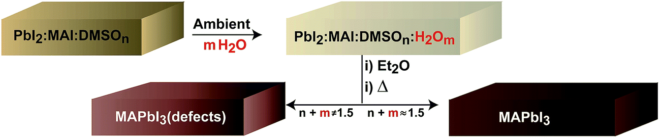 | ||
| Scheme 1 Schematic representation of key steps during the one-step fabrication process that takes into account the effect of ambient water. | ||
In order to provide understanding on the impact of additives (i.e. DMSO or H2O) on the morphology during perovskite generation several films were prepared under different conditions and were characterized by SEM analysis and absorbance measurements. Fig. 1 shows SEM images of representative films/devices fabricated using different DMSO:Pb ratios at constant R.H. (40%). Therefore, the proportion of H2O (m in Scheme 1) introduced in the system will be fixed. In the following discussion we refer to the DMSO:Pb ratio as a tool to modify the proportion n of DMSO in the complex as this will be the key parameter to control the crystallization as a function of humidity conditions. The top view image (Fig. 1a) of a device fabricated with a low proportion of DMSO (ratio 0.5) clearly shows a fiber-like morphology typical from materials fabricated from pure DMF.21,25,26 This result not only indicates that the proportion of DMSO is insufficient to generate the PbI2:MAI:additive complex but also reveals the presence of an uncovered electrode surface which will lead to the hole transport layer (HTL) to be in direct contact with the electron transport layer (ETL). As the DMSO proportion is increased to a DMSO:Pb ratio of 1.0 the complex is formed correctly as reported by Ahn et al.7 We observe a final morphology characterized by the presence of compact films with perovskite domains in the order of 100–500 nm (Fig. 1b). Therefore, the correct formation of the intermediate complex followed by the thermal treatment promotes the slow evaporation of the weakly bound DMSO providing the adequate morphology with a totally covered surface. Finally, a further increase of DMSO to a ratio of 1.5 (Fig. 1c) also leads to large crystalline domains similar to those in Fig. 1b. Interestingly, a large proportion of pinholes develops with cylindrical shape typical from gas evaporation from a quasi-solid state. Indeed, it is expected that the additional 0.5 mol of DMSO exceeding the adequate complex ratio will evaporate under the thermal treatment and the extra occupied volume will lead to voids in the film. The presence of domains with large differences in contrast is also noted. Light grey domains correspond to domains containing a large proportion of heavy atoms (i.e. Pb or I) and dark domains contain a larger proportion of lighter atoms such as carbon or oxygen like those expected from remaining DMSO in the films. We note that this type of morphology has recently been observed by Yang et al.27 using GBL/DMSO mixtures. In that case it was shown that an additional treatment with MABr was able to recover a morphology like the one shown in Fig. 1b. These results point to the possibility that multiiodide plumbates with the number of iodide ions <6 are being stabilized by DMSO and the MABr treatment is able to recover the PbX64− octahedra. The presence of bound DMSO will be confirmed below by absorption measurements. Analysis of the cross-section images (Fig. 1d–f) is quite revealing as the presence of pinholes in the perovskite layer is observed for devices fabricated with a PbI2:DMSO ratio of 0.5 and 1.5. These pinholes will inevitably lead to the direct contact between the spiro-OMeTAD and the mesoporous layer of TiO2 providing additional carrier recombination pathways, as it will be discussed in the final part of the manuscript.
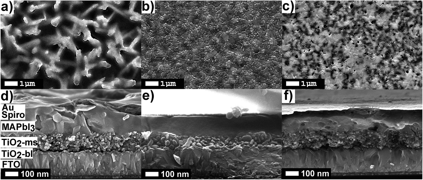 | ||
| Fig. 1 SEM images of devices fabricated at 40% R.H. using different DMSO:Pb ratios: 0.5 (a and d), 1.0 (b and e) and 1.5 (c and f). Top view (a–c) and cross-section (d–f). | ||
Alternatively, absorption measurements have been recently proved to be useful to detect chemical defects in perovskite films. Theoretical absorption bands of pure MAPbI3 are characterized by the presence of two bands at λmax ≈ 500 nm and λmax ≈ 760 nm as reported by de Angelis et al. using DFT calculations.28 Alternatively, experimental absorption bands of MAPbI3 films are usually more complex showing the presence of additional bands below 500 nm. Indeed, several species have been observed in films by different authors, such as PbIS5+, PbI2S4, PbI3S3−, PbI4S22−, PbI5S3−, PbI64− and (Pb2I4)n chains, all responsible for the bands in the region of ≈500 nm.21,25,29 Furthermore and to provide a complete picture of the absorbance response we also need to note that substrates partially covered by MAPbI3 films are characterized by strong scattering >750 nm. This observed scattering when measurements are carried out using regular spectrophotometers, as opposed to optical microscopy of single crystals, leads to artifacts decreasing the intensity of bands in the range of 250–750 nm.30
In this work, the absorption of MAPbI3 films is studied as a function of the DMSO:Pb ratio used in the precursor solution fabricated at R.H. = 40%, similar conditions to those used for the SEM analysis. Fig. 2a shows similar absorption band intensities in the 750 nm region for all films pointing to an equal thickness of the MAPbI3 layer. Alternatively, the absorption band intensity in the region of 350–550 nm strongly depends on the DMSO:Pb ratio. Films containing a ratio of 0.75 to 1.25 are very flat in the high energy region and are characterized by a morphology containing large crystalline domains as those shown in Fig. 1b with no pinholes. Alternatively, films with a fiber-like morphology (0.5 ratio, Fig. 1a) or presence of holes (1.5 ratio, Fig. 1c) show bands at 350–550 nm with increased intensity, just where several multiiodide plumbate species show their maximum absorbance. In particular, it appears that films containing high surface of grain boundaries do show increased intensities for multiplumbate ions such as PbI3S3−, PbI4S22−, PbI5S3−, PbI64− or (Pb2I4)n. During film formation the highly coordinating DMSO is able to stabilize the species as noted in the SEM image in Fig. 1c where the dark domains mostly appear around the holes indicating that DMSO remains in the film rather localized in this area. We note that a morphology with holes (Fig. 1c) leads to short PL decay time indicating that species associated with the grain boundaries play a very important role in the recombination pathways.27 Analysis of the precise proportion and the electrical effect of each of these species are beyond the scope of this work but in any case it appears difficult to separate physical and morphology effects.
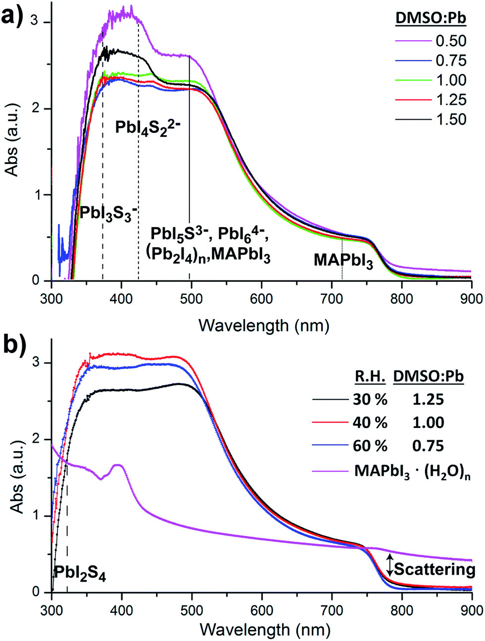 | ||
| Fig. 2 (a) Absorption spectra of MAPbI3 films measured as a function of the DMSO:Pb ratio used in the precursor solution, films fabricated at R.H. = 40%. (b) Absorption measurements of MAPbI3 films prepared under the optimum DMSO:Pb ratio under different humidity conditions. λmax for representative multiiodide plumbate ions are represented as vertical lines where S = solvent. Absorption spectrum of the hydrate complex. | ||
Relative humidity effect on chemical defects and electrical properties
There are some precedents in the literature of film formation under different humidity atmospheres paying special attention to the effect on the morphology. For example, Snaith et al. described generation of non-continuous morphologies under high R.H. with significantly improved photoluminescence and fast film formation.6 However, the correlation between generated species on films under humid environments and electrical properties has not been described. Here, we proceed to study the effect of water by modifying the relative humidity during processing of the devices. According to the process described in Scheme 1 and the competing displacement reactions described previously it is clear that water present in environmental humidity can be regarded as an additive which will affect the crystallization of the perovskite layer. For this purpose the DMSO:Pb ratio has been modified for films fabricated under different humidity conditions and complete absorption data are shown in the ESI.† Absorption results at 30% and 60% R.H. show similar trends as those observed in Fig. 2a with bands with an increased intensity in the 350–550 nm region when the amount of water and DMSO is not properly balanced to obtain the intermediate complex. Alternatively, it is very interesting to note that flat absorbance profiles in the region of 350–550 nm are only obtained when the DMSO/H2O concentration is controlled under given humidity conditions (Fig. 2b). This certainly agrees with the competitive process to coordinate the Pb core between DMSO and H2O. For example, as the humidity increases to R.H. = 60% a lower amount of DMSO is required to provide large crystalline domains as H2O is acting as an additive to form the PbI2:MAI:additive intermediate complex. Alternatively, when R.H. is reduced to 30% an increased amount of DMSO:Pb of 1.0–1.25 is required to obtain optimum morphology with a reduced amount of multiiodide plumbate defects.
The electrical properties of hydrate complexes can be monitored by preparing interdigitated electrodes containing perovskite hydrates. Here we follow a reported process to produce MAPbI3 hydrates from MAPbI3 films using a climatic chamber at R.H. = 80% and 60 °C for 60 min.17 Leguy et al. have optically characterized MAPbI3·H2O using ellipsometry measurements and showed the material to form nearly colorless needles. Needles of similar morphology as previously described are obtained as observed by SEM (Fig. 3a). The hydrate species generate wires of variable sizes but some exceeding lengths of 100 μm. A close inspection into the morphology shows that the wires are not totally compact. In addition, a picture of the film is shown in the ESI† where the white colour of the perovskite hydrate can be observed. The XRD spectra shown in the ESI† show some peaks which may be related to the MAPbI3·H2O complex (2θ = 25.4°, 28.4° and 31.9°) as compared with the theoretical powder spectra. In addition, some crystalline MAPbI3 domains indicate that the weakly bound water molecules have been released during the XRD measurement. Finally, degradation product PbI2 is also detected. However, other amorphous hydrate complexes may be present as well. Absorption spectra of the film are shown in Fig. 2b and high degree of scattering is observed above 750 nm which will reduce the intensity of bands below this wavelength value as described before. In any case a band is observed at 400 nm typical from PbI3S3− or PbI4S22 species and higher intensity bands appear below 350 nm that extends beyond 300 nm corresponding to species with still lower amount of iodides.
 | ||
| Fig. 3 (a) SEM image of an interdigitated electrode in the configuration Au/MAPbI3·(H2O)n/Au with a 200 μm channel. (b) Current–voltage curve of the interdigitated electrode in the configuration shown in (a) for devices containing either MAPbI3 or MAPbI3·(H2O)n. | ||
The electrical properties of the hydrate were probed in an interdigitated electrode configuration (Au/MAPbI3·(H2O)n/Au) with a 200 μm channel length on glass, see inset Fig. 3b. Using a similar configuration the conductivity of MAPbI3 has been measured by Johansson et al.31 and Müller et al. noted that conductivity increases with exposure to humid ambient conditions but pure films containing MAPbI3·(H2O)n hydrates have not been reported to this date.18 Current–voltage measurements were carried out under ambient conditions in the dark at scan rates of 100 mV s−1. I–V curves of MAPbI3 and MAPbI3·(H2O)n show ohmic behavior with higher currents for the monohydrate complex of nearly six order of magnitudes at ±1 V. We note that the stability of the interdigitated electrode containing MAPbI3·(H2O)n is low due to the large currents passing through the wires with a small diameter. Taking into account the device configuration the conductivity values of the perovskite in the order of 1 × 10⁻⁸ Scm−1 and 8 × 10⁻¹ Scm−1 are calculated, respectively. These results are in good agreement with previously reported results in interdigitated configuration and highlight the extreme sensitivity of the perovskites to the moisture environment. We also note that conductivity values have been calculated attending to the geometric area defined by the gold contacts/perovskite layer. However, the real active area relevant for the calculation will be much smaller as it is defined by the hydrate wires in direct contact with the gold electrode. Therefore, the provided conductivity value of MAPbI3·H2O only provides the low conductivity limit. In conclusion, the presence of hydrates will increase the conductivity of the perovskite layer several orders of magnitude and this will create alternative pathways for carriers to reach the contacts that may lead to shunting or a reduction of the selectivity of the contacts.
Impact of water and additives on photovoltaic devices
Now that the coordination chemistry of DMSO and H2O has been correlated with film formation morphology, absorbance and electrical properties, we proceed to analyze the effect of DMSO and H2O in photovoltaic devices. Devices are fabricated with the configuration FTO/TiO2-bl/TiO2-meso/MAPbI3/spiro-OMeTAD/Au where the DMSO:Pb ratio is varied for different series under humidity conditions. In order to be able to compare with the previous sections of the manuscript the same processing conditions have been used and results are the same. Each data point shown in Fig. 4 corresponds to an average of 20 independent devices measured under reverse bias sweep at a scan rate of 50 mV s−1. Overall, the device efficiency can be increased from 10.8% to 18.6% by carefully adjusting the DMSO:Pb ratio attending to the R.H.
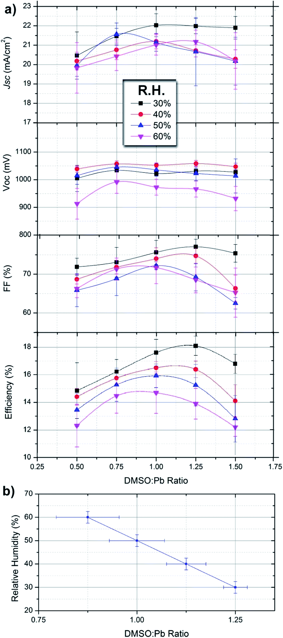 | ||
| Fig. 4 (a) Efficiency parameters of devices fabricated with the configuration FTO/TiO2-bl/TiO2-meso/MAPbI3/spiro-OMeTAD/as a function of the DMSO:Pb ratio used in the precursor solution fabricated under different relative humidity conditions. Each data point corresponds to 20 independent devices. (b) Observed maximum efficiency as a function of relative humidity and DMSO:Pb ratio. | ||
Under given humidity conditions we observe that the photocurrent (Jsc) of devices varies from ≈20–22 mA cm−2 with the DMSO:Pb being higher for ratios between 0.75 and 1.25. Increased photocurrents are the result of an adequate morphology containing large crystalline domains with little presence of chemical impurities in the films. Lower photocurrents are obtained with devices at either a low or high DMSO:Pb ratio as a result of inadequate morphology (Fig. 1a and c) and the presence of multiiodide plumbate species (Fig. 2a). Note that absolute absorbance values are higher for films fabricated with low and high DMSO:Pb ratios (Fig. 2a) but photocurrents are lower indicating that the presence of the chemical species is related to recombination pathways. Alternatively, under the highest humidity conditions the achievable photocurrent decreases indicating that the perovskite hydrate leads to increased recombination pathways. The open-circuit potential (Voc) of the devices is rather insensitive to the DMSO:Pb ratio and seems to be more connected to the humidity conditions. Indeed, devices fabricated at R.H. = 60% show Voc about 100 mV lower than those fabricated under low R.H. The highly conductive nature of the MAPbI3·(H2O)n hydrates has been shown. Then, it is clear that the hydrate can act as charge carrier percolation pathways leading to shunting of the devices. This effect is more severe under low DMSO proportion (ratio of 0.5) where synthesis of the hydrate complex is maximized by the reduction of competing molecules. Indeed, shunting pathways are already observed in the SEM cross-section of Fig. 1d. The fill Factor (FF) of devices shows a similar trend to that of Jsc ranging from 60 to 78 depending on the processing conditions, this difference represents a 25% increase under adequate conditions. In this regard increased DMSO and H2O proportions during the processing conditions of the device lead to the lowest values. Therefore, it appears that not only the film morphology needs to be adequate but there should not be any excess of highly coordinating molecules as they seem to increase all recombination processes.
Very interestingly, under each humidity condition the maximum efficiency can be maximized by tuning the DMSO:Pb ratio to obtain the correct intermediate complex stoichiometry. For example, at R.H. of 30% the observed optimum DMSO:Pb ratio is 1.25 providing highest efficiencies in the series of 18.7% (Voc = 1.05 V, Jsc = 22.4 mA cm−2 and FF = 78). Under given humidity conditions the required DMSO:Pb ratio to provide maximum efficiencies decreases as the R.H. increases. Indeed, at R.H. = 60% ratios of 0.75–1.00 offer maximum efficiencies of ≈14.5% (Voc = 1.00 V, Jsc = 20.5 mA cm−2 and FF = 72). This result clearly indicates that competition between DMSO and H2O molecules is readily taking place following coordination chemistry reactions as those discussed previously. Interestingly, absorbance spectra of films providing the highest efficiency under each R.H. (Fig. 2b) are flat in the range of 350–550 nm indicating that the presence of multiiodide plumbate ions is minimized. It is important to highlight that error bars are larger when a low proportion of DMSO is used due to the presence of pinholes. The reduction in Jsc and Voc in the presence of vapour water molecules is in agreement with the work by Leguy et al. as they observed up to a 90% decrease in short-circuit photocurrent and ∼200 mV loss in open-circuit potential Voc during degradation experiments.17 In addition, extrapolation of the linear tendency observed in Fig. 4b can also be used to calculate the ideal proportion of additives in a situation where no water is present (i.e. in a glovebox) providing the values of n + m ≈ 1.5 used in different parts of the manuscript.
From this data we note that the presence of water is generally negative for the final device performance but its effect can be minimized by correctly formulating the precursor solution. Indeed, higher efficiencies are obtained for devices prepared under low R.H. but in all cases the DMSO:Pb ratio needs to be adjusted to provide maximum efficiencies. Very importantly, Fig. 4b offers reference data for the reader to implement in their own processes taking into account different humidity conditions. In addition, we noted that stability of devices prepared at 60% R.H. was somehow lower than those prepared under 30% R.H. during characterization under light and voltage conditions. However, further complete studies are required to confirm these preliminary results.
Conclusions
In the field of lead halide perovskite solar cells highest reported efficiencies are typically obtained for layers processed under a totally dry environment that ultimately increases the production costs. This manuscript presents new insights to minimize the negative effect of environmental water enabling the processing of solar cells in ambient air with high efficiencies and reproducibility. It is shown that the H2O/DMSO ratio needs to be carefully adjusted to obtain adequate morphology and to reduce the presence of chemical defects. Both molecules compete to coordinate with the Pb atom which will limit the formation of the intermediate complex PbI2:MAI:additive responsible for the final properties of the films. High efficiency devices processed in air with a PCE approaching 19% can be obtained for the simplest perovskite formulation MAPbI3 under different humidity conditions.
Acknowledgements
We thank MINECO of Spain for their financial support under project (MAT2013-47192-C3-1-R), and Generalitad Valenciana is acknowledged for financial support on the DISOLAR2 Project (PROMETEOII/2014/020). A. G. would like to thank the Spanish Ministerio de Economía y Competitividad for a Ramón y Cajal Fellowship (RYC-2014-16809). C. L. and S. H. thank the Bavarian framework project SOLTECH for funding. Serveis Centrals at UJI (SCIC) is acknowledged for the SEM measurement assistance.References
- M. A. Green, K. Emery, Y. Hishikawa, W. Warta and E. D. Dunlop, Prog. Photovoltaics, 2015, 23, 1–9 Search PubMed.
- M. Saliba, T. Matsui, K. Domanski, J.-Y. Seo, A. Ummadisingu, S. M. Zakeeruddin, J.-P. Correa-Baena, W. R. Tress, A. Abate, A. Hagfeldt and M. Grätzel, Science, 2016, 354, 206–209 CrossRef CAS PubMed.
- J. P. Correa Baena, L. Steier, W. Tress, M. Saliba, S. Neutzner, T. Matsui, F. Giordano, T. J. Jacobsson, A. R. Srimath Kandada, S. M. Zakeeruddin, A. Petrozza, A. Abate, M. K. Nazeeruddin, M. Gratzel and A. Hagfeldt, Energy Environ. Sci., 2015, 8, 2928–2934 CAS.
- H. Zhou, Q. Chen, G. Li, S. Luo, T.-b. Song, H.-S. Duan, Z. Hong, J. You, Y. Liu and Y. Yang, Science, 2014, 345, 542–546 CrossRef CAS PubMed.
- J. You, Y. Yang, Z. Hong, T.-B. Song, L. Meng, Y. Liu, C. Jiang, H. Zhou, W.-H. Chang and G. Li, Appl. Phys. Lett., 2014, 105, 183902 CrossRef.
- G. E. Eperon, S. N. Habisreutinger, T. Leijtens, B. J. Bruijnaers, J. J. van Franeker, D. W. deQuilettes, S. Pathak, R. J. Sutton, G. Grancini, D. S. Ginger, R. A. J. Janssen, A. Petrozza and H. J. Snaith, ACS Nano, 2015, 9, 9380–9393 CrossRef CAS PubMed.
- N. Ahn, D.-Y. Son, I.-H. Jang, S. M. Kang, M. Choi and N.-G. Park, J. Am. Chem. Soc., 2015, 137, 8696–8699 CrossRef CAS PubMed.
- M. I. Saidaminov, A. L. Abdelhady, B. Murali, E. Alarousu, V. M. Burlakov, W. Peng, I. Dursun, L. Wang, Y. He, G. Maculan, A. Goriely, T. Wu, O. F. Mohammed and O. M. Bakr, Nat. Commun., 2015, 6, 7586 CrossRef PubMed.
- Y.-J. Jeon, S. Lee, R. Kang, J.-E. Kim, J.-S. Yeo, S.-H. Lee, S.-S. Kim, J.-M. Yun and D.-Y. Kim, Sci. Rep., 2014, 4, 6953 CrossRef CAS PubMed.
- P.-W. Liang, C.-Y. Liao, C.-C. Chueh, F. Zuo, S. T. Williams, X.-K. Xin, J. Lin and A. K. Y. Jen, Adv. Mater., 2014, 26, 3748–3754 CrossRef CAS PubMed.
- Y. Wu, A. Islam, X. Yang, C. Qin, J. Liu, K. Zhang, W. Peng and L. Han, Energy Environ. Sci., 2014, 7, 2934–2938 CAS.
- D. Shi, V. Adinolfi, R. Comin, M. Yuan, E. Alarousu, A. Buin, Y. Chen, S. Hoogland, A. Rothenberger and K. Katsiev, Science, 2015, 347, 519–522 CrossRef CAS PubMed.
- P. K. Nayak, J. Bisquert and D. Cahen, Adv. Mater., 2011, 23, 2870–2876 CrossRef CAS.
- W. S. Yang, J. H. Noh, N. J. Jeon, Y. C. Kim, S. Ryu, J. Seo and S. I. Seok, Science, 2015, 348, 1234–1237 CrossRef CAS PubMed.
- C.-G. Wu, C.-H. Chiang, Z.-L. Tseng, M. K. Nazeeruddin, A. Hagfeldt and M. Gratzel, Energy Environ. Sci., 2015, 8, 2725–2733 CAS.
- L. Li, Y. Chen, Z. Liu, Q. Chen, X. Wang and H. Zhou, Adv. Mater., 2016, 28, 9862–9868 CrossRef CAS PubMed.
- A. M. A. Leguy, Y. Hu, M. Campoy-Quiles, M. I. Alonso, O. J. Weber, P. Azarhoosh, M. van Schilfgaarde, M. T. Weller, T. Bein, J. Nelson, P. Docampo and P. R. F. Barnes, Chem. Mater., 2015, 27, 3397–3407 CrossRef CAS.
- C. Müller, T. Glaser, M. Plogmeyer, M. Sendner, S. Döring, A. A. Bakulin, C. Brzuska, R. Scheer, M. S. Pshenichnikov, W. Kowalsky, A. Pucci and R. Lovrinčić, Chem. Mater., 2015, 27, 7835–7841 CrossRef.
- W. Zhou, Y. Zhao, C. Shi, H. Huang, J. Wei, R. Fu, K. Liu, D. Yu and Q. Zhao, J. Phys. Chem. C, 2016, 120, 4759–4765 CAS.
- J. M. Frost, K. T. Butler, F. Brivio, C. H. Hendon, M. van Schilfgaarde and A. Walsh, Nano Lett., 2014, 14, 2584–2590 CrossRef CAS PubMed.
- Y. Guo, K. Shoyama, W. Sato, Y. Matsuo, K. Inoue, K. Harano, C. Liu, H. Tanaka and E. Nakamura, J. Am. Chem. Soc., 2015, 137, 15907–15914 CrossRef CAS PubMed.
- J. You, L. Meng, T.-B. Song, T.-F. Guo, Y. M. Yang, W.-H. Chang, Z. Hong, H. Chen, H. Zhou, Q. Chen, Y. Liu, N. De Marco and Y. Yang, Nat. Nanotechnol., 2016, 11, 75–81 CrossRef CAS PubMed.
- J. H. Heo, D. H. Song and S. H. Im, Adv. Mater., 2014, 26, 8179–8183 CrossRef CAS PubMed.
- K. Domanski, J.-P. Correa-Baena, N. Mine, M. K. Nazeeruddin, A. Abate, M. Saliba, W. Tress, A. Hagfeldt and M. Grätzel, ACS Nano, 2016, 10, 6306–6314 CrossRef CAS PubMed.
- S. Rahimnejad, A. Kovalenko, S. Martí-Forés, C. Aranda and A. Guerrero, ChemPhysChem, 2016, 17, 2795 CrossRef CAS PubMed.
- E. Horváth, M. Spina, Z. Szekrényes, K. Kamarás, R. Gaal, D. Gachet and L. Forró, Nano Lett., 2014, 14, 6761–6766 CrossRef PubMed.
- M. Yang, T. Zhang, P. Schulz, Z. Li, G. Li, D. H. Kim, N. Guo, J. J. Berry, K. Zhu and Y. Zhao, Nat. Commun., 2016, 7, 12305 CrossRef CAS PubMed.
- P. Umari, E. Mosconi and F. De Angelis, Sci. Rep., 2014, 4, 4467 Search PubMed.
- K. Yan, M. Long, T. Zhang, Z. Wei, H. Chen, S. Yang and J. Xu, J. Am. Chem. Soc., 2015, 137, 4460–4468 CrossRef CAS PubMed.
- Y. Tian and I. G. Scheblykin, J. Phys. Chem. Lett., 2015, 6, 3466–3470 CrossRef CAS PubMed.
- K. Sveinbjörnsson, K. Aitola, X. Zhang, M. Pazoki, A. Hagfeldt, G. Boschloo and E. M. J. Johansson, J. Phys. Chem. Lett., 2015, 6, 4259–4264 CrossRef PubMed.
Footnotes |
| † Electronic supplementary information (ESI) available: Methods, further absorption measurements, and XRD data. See DOI: 10.1039/c6se00077k |
| ‡ Both authors contributed equally. |
| This journal is © The Royal Society of Chemistry 2017 |