
The role of layer-by-layer, compact TiO2 films in dye-sensitized photoelectrosynthesis cells†
Rodolfo L.
Coppo
a,
Byron H.
Farnum
b,
Benjamin D.
Sherman
b,
Neyde Y.
Murakami Iha
*a and
Thomas J.
Meyer
 *b
*b
aLaboratory of Photochemistry and Energy Conversion, Departamento de Química Fundamental, Instituto de Química, Universidade de São Paulo-USP, Av. Prof. Lineu Prestes, 748, 05508-900 São Paulo, SP, Brazil. E-mail: neydeiha@iq.usp.br
bDepartment of Chemistry, University of North Carolina at Chapel Hill, Chapel Hill, NC 27599, USA. E-mail: tjmeyer@unc.edu
First published on 9th January 2017
Abstract
A new insight into improving dye-sensitized photoelectrosynthesis cells (DSPECs) is reported here by using layer-by-layer deposition of compact nanoTiO2 films. These compact films were obtained by a sol–gel method and deposited on conductive glass substrates, beneath a nanoITO/TiO2 core/shell (ITO: tin-doped indium oxide) mesoporous network. The performance of DSPECs having the nanoTiO2-modified photoanode was evaluated and a remarkable enhancement of 53% in photocurrent was achieved, as well as cathodic currents shifted to more negative potentials. The compact TiO2 films on FTO (fluorine-doped tin oxide) improve the contact between core/shell network and conductive glass, and provide an enhanced collection of electrons at the photoanode, achieving a significant advance in DSPEC performance.
Introduction
New concepts in artificial photosynthesis are offering additional approaches to the storage of chemical energy in chemical bonds.1,2 One approach is the dye-sensitized photoelectrosynthesis cell (DSPEC). It comes from chemical concepts used in dye-sensitized solar cells (DSCs),3–9 and uses architectures/materials with chromophore/catalyst assemblies10,11 attached to oxides such as TiO2,12 SnO2,13 or nanoITO (tin-doped indium oxide)12 for light harvesting. After four cycles of photon absorption, the device generates oxygen and H+ at the photoanode; H+ diffuses to a separate cathode for reduction to hydrogen gas.Although promising, the efficiencies of these devices are low. They are limited by interfacial back electron transfer within the mesoporous structure, back electron transfer to a surface-bound catalyst, or low rate of transport of collected electrons to the FTO (fluorine-doped tin oxide) electrode. Decreasing back electron transfer to the chromophore-catalyst is one of the strategies that have been exploited for improving DSPEC efficiencies using metal oxide outer layers of TiO2![[thin space (1/6-em)]](https://www.rsc.org/images/entities/char_2009.gif) 12,14 or Al2O313 in core/shell structures deposited conformally by atomic layer deposition (ALD). ALD gives thin 3–5 nm shells on the surfaces of 4–15 micron mesoporous films with electron transfer back to the outer shells inhibited by internal bias effects.2,12,13
12,14 or Al2O313 in core/shell structures deposited conformally by atomic layer deposition (ALD). ALD gives thin 3–5 nm shells on the surfaces of 4–15 micron mesoporous films with electron transfer back to the outer shells inhibited by internal bias effects.2,12,13
Another example of increasing electron collection at the photoanode comes from deposition of thin oxide films, on FTO under the mesoporous network, acting as blocking and/or contact layers in DSCs.15–17 Nanostructured TiO2 is a suitable material due to its high optical transmittance, high dielectric constants and high refractive index.18,19 Many TiO2 deposition methods such as ALD,20,21 chemical vapor deposition (CVD),18,21 spray pyrolysis,15 and Layer-by-Layer assembly formation (LbL)22,23 have been reported. LbL is a low-cost technique, that gathers the simplicity of TiO2 prepared by a sol–gel method with low cost processing and suitable control of thickness by varying the number of bilayers.22 We have used this approach in DSCs22–26 improving device efficiencies by up to 62%.22
Here we report, for the first time, an extension to an LbL-TiO2-modified DSPEC based on the assembly shown in Fig. 1. LbL films were characterized by scanning electron microscopy (SEM), atomic force microscopy (AFM), and device performance was assessed by photocurrent–time measurements, incident photon-to-current efficiencies (IPCE), linear voltammetry, voltage decay, and electron lifetimes. The results of these measurements reveal a significant increase in device efficiency by appropriate modification of the inner layer by using LbL compact films.
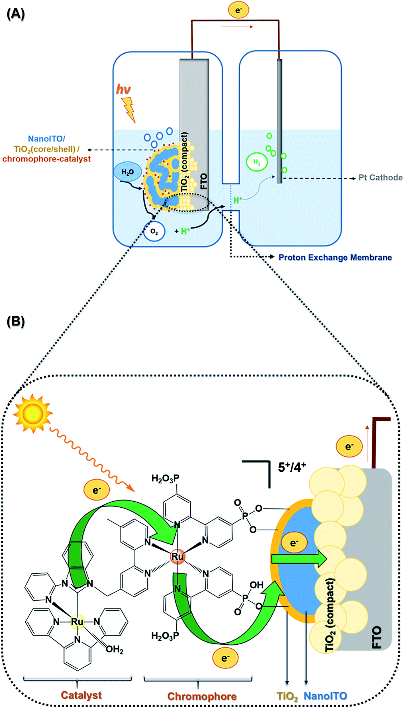 | ||
| Fig. 1 (A) Architecture of a DSPEC assembled with compact layers (Ag/AgCl reference electrode is not shown); (B) photon absorption, electron injection and transport, and catalyst oxidation in the FTO|compact layers|nanoITO/TiO2|chromophore-catalyst-1 electrode. | ||
Experimental
TiO2 preparation and deposition on FTO
TiO2 nanoparticles were synthesized by sol–gel methods22,23,25 by acidic and basic hydrolysis. Under acidic conditions, 24 mL of titanium(IV) isopropoxide (Sigma-Aldrich) was added dropwise in 140 mL of 0.10 mol L−1 HNO3 aqueous solution (Milli-Q purified water) under stirring in an ice bath. Under basic conditions, hydrolysis was carried out with the same titanium precursor, using 0.10 mol L−1 NH4OH aqueous solution. Both systems were stirred and heated at 80.0 °C for 8 h for the peptization process, resulting in suspensions of TiO2(acidic) and TiO2(basic). TiO2(acidic) sol (pH ∼2) concentration was checked by a thermogravimetric method and diluted to 25 mg mL−1 with 0.10 mol L−1 HNO3 aqueous solution. The TiO2(basic) suspension was filtered and the sol was used without any adjustment (3.0 mg mL−1, pH ∼9).TiO2(acidic) and TiO2(basic) sols were deposited by Layer-by-Layer (LbL) technique22 onto FTO (TEC-15, 15 Ω □−1, Hartford Glass Inc.) cleaned by sonication in ∼0.10 mol L−1 HCl in ethanol for 20 min and dried under air. The substrate was dip coated alternately for 5 min in each TiO2 sol, washed with Milli-Q water (2 min) and dried under air between acidic and basic deposition cycles to result in one bilayer (BL), Scheme 1; cycles were repeated to produce 1, 3 and 5 BL on FTO surfaces.
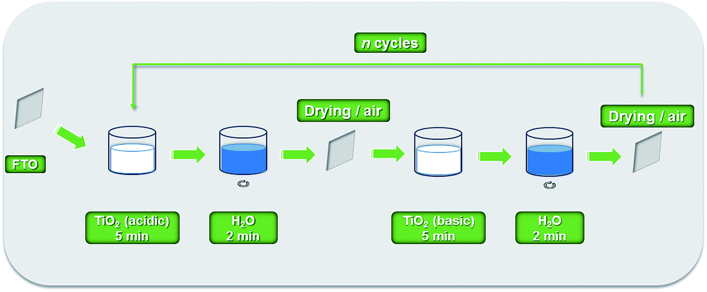 | ||
| Scheme 1 Compact TiO2 films assembly by the LbL technique. | ||
NanoITO electrode fabrication
1.3 g of hydroxypropyl cellulose (HPC, Sigma-Aldrich, average Mw = 80000, 20 mesh particle size) was added to 15 mL of ethanol (Decon Labs) followed by overnight stirring. 2 mL of 30 wt% nanoITO (tin-doped indium oxide) dispersion in ethanol (TC8 DE, Evonik Industries) was bath sonicated for 20 min. 2 mL of the 10 wt% HPC suspension was added to nanoITO suspension and stirred overnight. A tape (Kapton) was applied to one edge of FTO to define an area of 1.0 cm2. NanoITO paste (∼4 μm thickness) was applied by painting onto substrates with and without the compact TiO2 layers. The thin films were annealed in a furnace (Blue M, Thermo Scientific Lindberg) at 500 °C for 1 h.
TiO2 core/shell network
Atomic layer deposition (ALD) was performed in a Savannah S200 (Cambridge Nanotech) reactor on nanoITO electrodes. The precursor tetrakis(dimethylamido)titanium (TDMAT, 99.999%, Sigma-Aldrich) was heated in its reservoir at 75 °C for 1 h. ALD coating conditions were carried out with modification of previously reported procedure,13 under 150 °C and 14 torr of N2 carrier gas using a sequence of 0.5 s metal precursor dose, 20 s hold, 20 s N2 purge, 0.015 s H2O dose, 20 s hold, 20 s N2 purge. The 60 cycle-deposition resulted in a shell thickness of 3.4 nm, checked by ellipsometry in a V-Vase Ellipsometer (J.A. Woollam Co Inc).Photoanode
NanoITO|TiO2(core/shell) electrodes were derivatized by ∼16 h immersion into 0.10 mol L−1 HNO3 solutions containing ∼10−5 to 10−4 mol L−1 chromophore-catalyst: [((PO3H2)2bpy)2Ru(4-Mebpy-4′-bimpy)Ru(tpy)(OH2)]4+ (1), (PO3H2)2bpy = 4,4′-bisphosphonato-2,2′-bipyridine; 4-Mebpy-4′-bimpy = 4-(methylbipyridin-4′-yl)-N-benzimid-N′-pyridine; tpy = 2,2′:6′,2′′-terpyridine.LbL TiO2 film characterization
Morphological characterization of the films was performed by atomic force microscopy (AFM) using an MFP-3D microscope (Asylum Research) and the images were registered under non-contact mode. Surfaces were also investigated by scanning electron microscopy (SEM) using a S-4700 microscope (Hitachi) with acceleration voltage of 2 kV for imaging. Samples were coated with <2 nm AuPd. The components at the interface compact layer/FTO were identified by energy-dispersive X-ray spectroscopy (EDS) using a INCAPentaFETx3 microscope (Oxford) with acceleration voltage. Samples were coated with AuPd.Photoelectrochemical measurements
Experiments were carried out with DSPECs using a FTO|compact layers|nanoITO/TiO2(core/shell)|chromophore-catalyst-1 photoanode and compared with similar assemblies without compact layers. Photoelectrochemical experiments were performed with a CHI 760E potentiostat (CH Instruments) in 20 mmol L−1 acetate buffer at pH 4.6 with the ionic strength adjusted to 0.50 mol L−1 with LiClO4.12 Pt wire (or graphite) and Ag/AgCl were used as counter and reference electrodes, respectively, applying 200 mV bias. Irradiation at 445 nm (FWHM 20 nm) was provided by a solid state LED (Lumencor) or white light source (HPLS-30-04, Thor Labs) with a GG 400 long pass UV blocking filter (Newport).Absorption spectra
Absorption spectra were obtained in an 8453 diode array Hewlett-Packard Spectrophotometer.Results and discussion
Fig. 1(A) shows the DSPEC configuration, as well as the electrode, FTO|compact layers|nanoITO/TiO2(core/shell)|chromophore-catalyst-1, derivatized on a core/shell structure of nanoITO/TiO2. Fig. 1(B) focuses on the photoanode structure, depicting the LbL compact film deposited on FTO under mesoporous oxide, including dynamics of photon absorption, electron injection/transport, and catalyst oxidation.LbL TiO2 film characterization
The morphologies of the films were assessed by Atomic Force Microscopy (AFM) non-contact mode, Fig. 2(A), and Scanning Electron Microscopy (SEM), Fig. 2(B).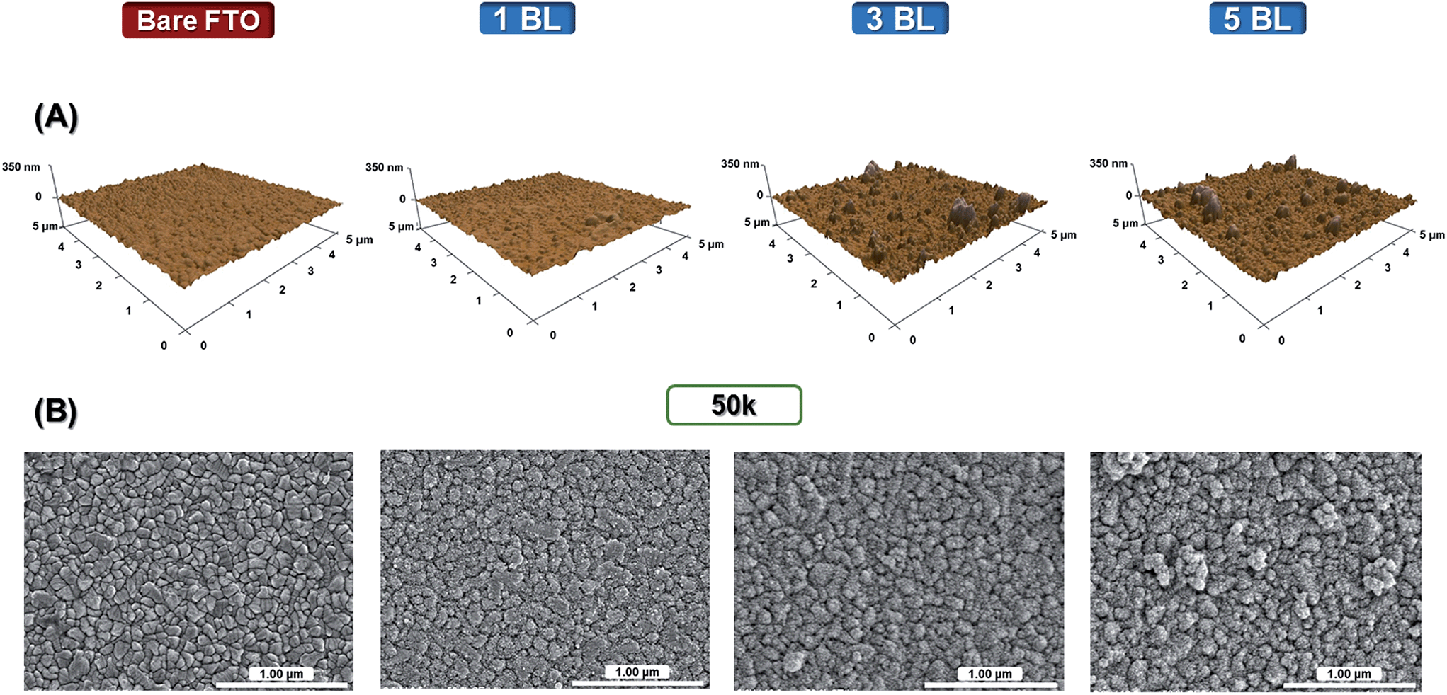 | ||
| Fig. 2 (A) AFM (scan size: 5 × 5 μm) and (B) SEM images (magnification: 50000×) for bare FTO and TiO2 bilayers (BL) deposited onto FTO prior to sintering. | ||
Morphological changes on the FTO surface were evidenced by the increase in the number of bilayers (BL), with films composed of densely packed nanoparticle layers and some aggregates. One can observe a reasonably compact structure even with a single bilayer of TiO2 in films that partially covers the sharp crystallite facets of FTO. The root-mean-square (rms) roughness data – measured by AFM software – and the FTO surface patterns are similar for both bare FTO and a single BL film, with exposure of the conductive nanoparticles of the same rms, 13 nm. With the thickness increased to 34 nm (3 BL), the surface is highly compact and fully covered by the LbL TiO2 films with the rms of 28 nm, maintained up to 5 BL.
The LbL technique consists of a sequential adsorption of positively and negatively charged nanoparticles with cyclic depositions, possible because of charge compensation between the nanoparticles, with electrostatic and van der Waals attractive forces occurring.27 During the synthesis of TiO2 nanoparticles, stepwise hydrolysis and condensation steps lead to three dimensional polymeric Ti–O–Ti chains.22 In these chains, oxygen sites are protonated in the acidic route, and negatively charged in the alkaline route.
The morphology of TiO2(acidic) and TiO2(basic) films is characterized by densely-packed layers of nanoparticles with interaction between nanoparticles that leads to aggregation as evidenced in the AFM images. This characteristic has also been reported previously in inorganic nanoparticles paired with high molar weight polyelectrolytes, examples being acidic TiO2 and sodium sulfonated polystyrene, sulfonated lignin and poly(acrylic acid).25
Energy-dispersive X-ray spectroscopy, Fig. S1,† depicts the composition of the compact TiO2 layer on FTO with Ti peaks appearing at 0.53, 4.52 and 4.93 keV, consistent with Ti standards.22 The remaining peaks can be assigned to other components in the FTO substrate or PdAu coating.
DSPEC performance
Fig. 3 shows short term J–t profiles for DSPECs based on (1) with different numbers of LbL compact layers beneath the nanoITO/TiO2 core/shell assembly with a comparison of photocurrents without the added compact layer. All of the curves were corrected for the fraction of light absorbed (absorptance) by the chromophore-catalyst assembly (1), by deducting the effect of the FTO|compact layers|nanoITO/TiO2 for each photoanode.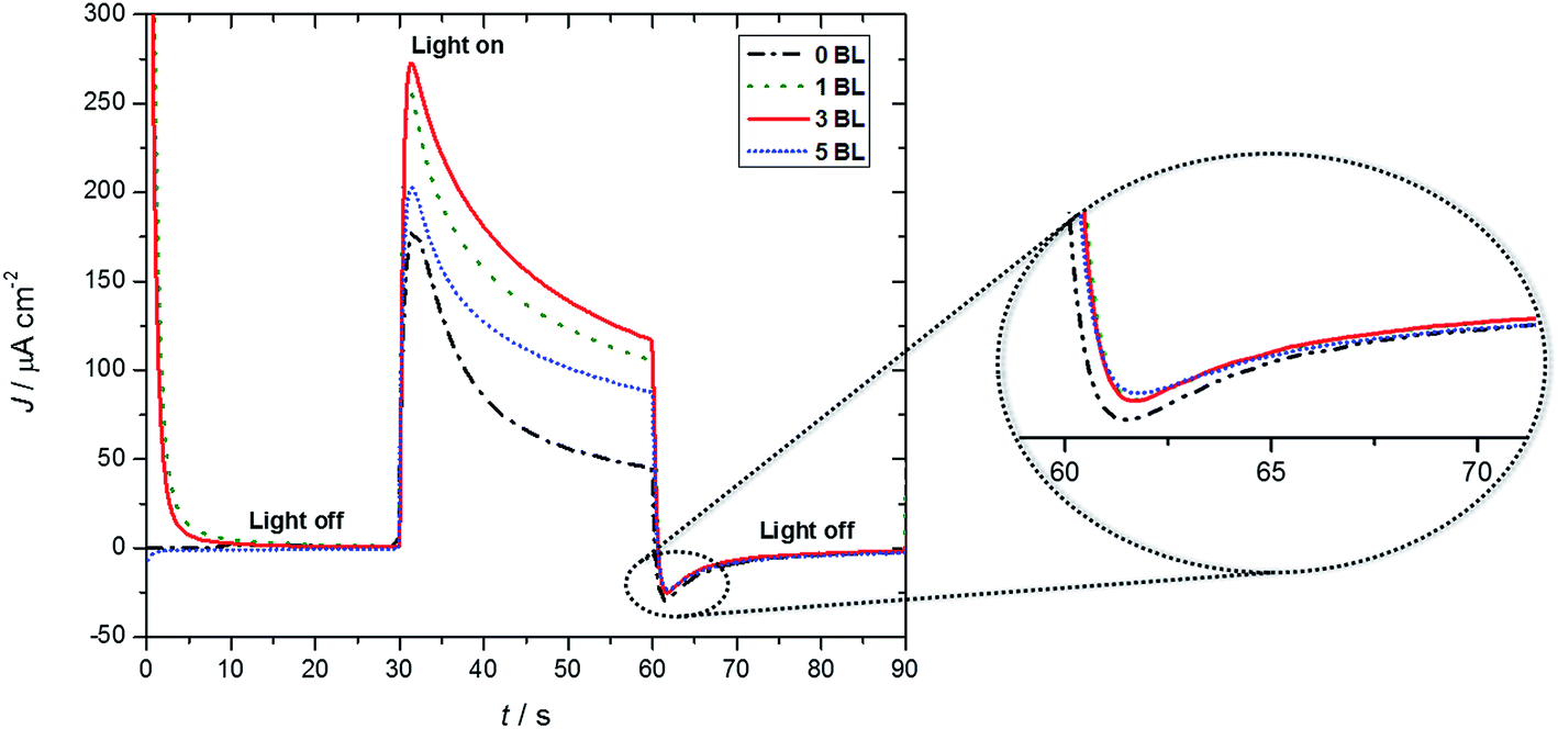 | ||
| Fig. 3 J–t curves for FTO|nanoITO/TiO2|-1 assemblies with and without compact layers deposited by LbL (20 mmol L−1 acetate buffer, pH 4.6, 0.50 mol L−1 LiClO4, λ = 445 nm, biased at 200 mV vs. Ag/AgCl). | ||
The initial photocurrent spikes in the curves arise from Ru dimer oxidation to its steady-state form, –[RuIIa–RuIVb![[double bond, length as m-dash]](https://www.rsc.org/images/entities/char_e001.gif) O]4+, and to capacitance effects.13,28 Additional 1 e− oxidation to –[RuIIIa–RuIVb(O)]4+ is followed by addition of water, which is rate limiting, give the transient intermediate –[RuIIa–RuIVb(OO)]4+. It undergoes further oxidation, loss of O2, and re-integration into the catalytic cycle.29 At the end of the initial 30 s photolysis period, a characteristic small cathodic current is observed arising from core/shell layer to partly oxidized chromophore-catalyst.
O]4+, and to capacitance effects.13,28 Additional 1 e− oxidation to –[RuIIIa–RuIVb(O)]4+ is followed by addition of water, which is rate limiting, give the transient intermediate –[RuIIa–RuIVb(OO)]4+. It undergoes further oxidation, loss of O2, and re-integration into the catalytic cycle.29 At the end of the initial 30 s photolysis period, a characteristic small cathodic current is observed arising from core/shell layer to partly oxidized chromophore-catalyst.
Photocurrent comparisons reported here were for 30 seconds of irradiation, biased at 200 mV. The currents stabilize and then slowly decrease over longer periods (minutes) due to slow decomposition of the catalyst.29 Based on the data in Fig. 3, the maximum initial photocurrent of 272 μA cm−2 for the DSPEC with 3 BL falls to 117 μA cm−2. For the photoanode without the compact TiO2 layer, under the same conditions, a peak current of 178 μA cm−2 was observed, which decreased to 45 μA cm−2. Analysis of the data showed that the 3 BL compact film was responsible for a 53% increase in photocurrent compared to samples without a compact layer (Table 1). This outstanding photocurrent improvement was also observed by Zanoni, Amaral and Murakami Iha22 in DSCs using compact TiO2 films with different thicknesses and were assigned to a blocking and contact effect in LbL TiO2 modified devices.
Additional observations point to stabilization enhancements by the compact TiO2 layers. After a 30 second, light on photolysis period, photocurrent decreases of ∼2.3× were observed for all photoanodes with compact TiO2 films (note results for a 200 s experiment in Fig. S2†). There was a decrease of ∼4× for the sample with no compact layer. There is also evidence that film thickness near tunneling/transport layer might play role for a compact layer of 5 BL with a 203 μA cm−2 photocurrent level.
Dark currents at the end of light-on/light-off cycles observed immediately after light is turned off (note the zoom in Fig. 3) for DSPECs modified with 1, 3 and 5 BL are different from the DSPEC without BL, suggesting a blocking effect, provided by the compact layers.
Incident photon-to-current efficiencies (IPCE), Fig. 4, confirm the role of 3 BL in the DSPEC response. Substantial differences between samples with and without compact layers are observed, specially in the absorption region of the chromophore-catalyst assembly (Fig. S3†).
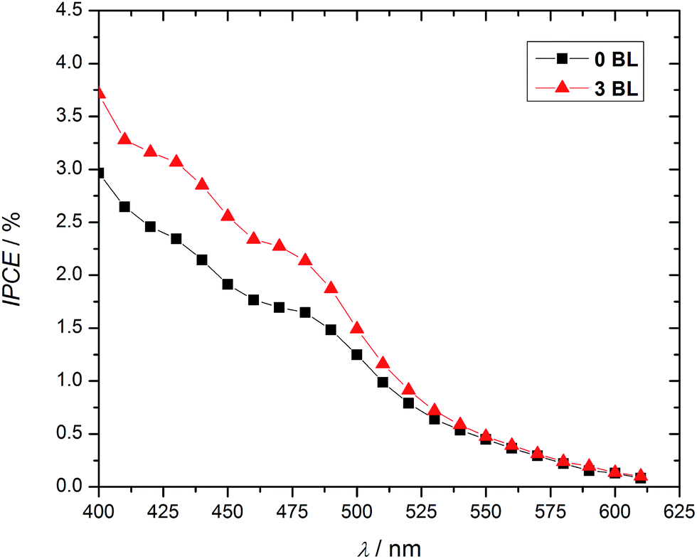 | ||
| Fig. 4 IPCE enhancements for DSPECs with 34 nm (3 BL) compact TiO2 layers (20 mmol L−1 acetate buffer, pH 4.6, 0.50 mol L−1 LiClO4, biased at 200 mV vs. Ag/AgCl). | ||
IPCE is related to light harvesting efficiency, LHE, charge collection efficiency, ηc, and charge injection efficiency across the solid–liquid interface, ηinterface, as shown in eqn (1).30–32 Assuming constant LHE and injection efficiencies at the photoanodes with and without 3 BL, the data demonstrate a significant impact on collection efficiency for 3 BL DSPEC.
| IPCE (%) = LHE × ηc × ηinterface | (1) |
The bias dependence for the half cell is shown in Fig. 5 and features cathodic currents for DSPEC with and without 3 BL. Under dark conditions, a difference of ∼50 mV is observed, with both samples reaching −25 μA cm−2, with the compact layers responsible for the shift to more negative potentials. Under irradiation, a similar trend is observed, although with a smaller effect. As the coverage of the TiO2 layer on FTO becomes effective, an insulating effect occurs at or near the conduction band edge preventing transfer of collected charges to oxidized species immobilized on the mesoporous oxide surface. This may lead to higher oxygen evolution efficiencies.
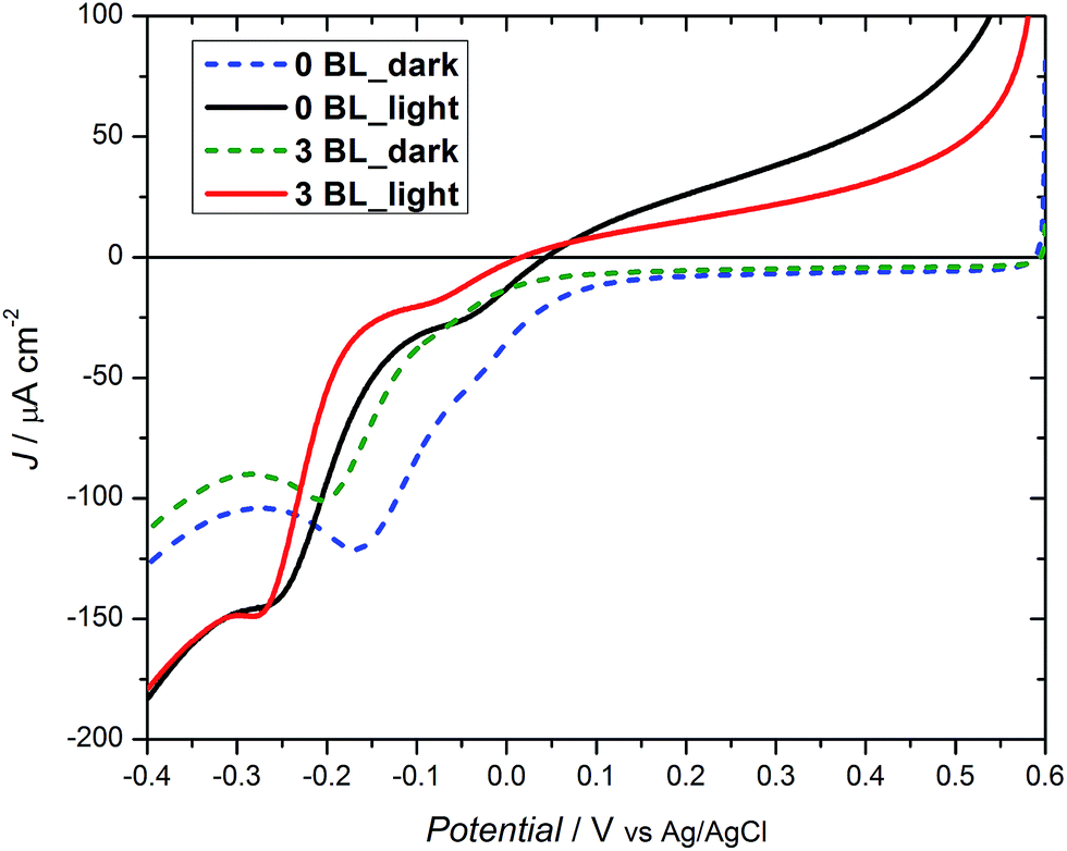 | ||
| Fig. 5 Linear sweep voltammograms for DSPECs with 0 BL and 3 BL (20 mmol L−1 acetate buffer, pH 4.6, 0.50 mol L−1 LiClO4vs. Ag/AgCl). | ||
Electron recombination measurements (VOC decay) have been extensively used to assess electron recombination in DSC devices14,20,22,33 and were extended here to the operating DSPEC. At the end of a photolysis period, the Fermi level (EF) at the anode reaches the redox potential of the solution. Fig. 6(A) illustrates the variation in EF decay with and without the compact layer. No substantial differences were observed in their shapes, which were different from those obtained with DSCs,14,22 where visible changes in the kinetics had been observed with added layers. The difference in response arises since the DSPEC device contain no redox mediators. After a photolysis period, the catalyst is returned to its steady state with a small amount of O2 released to the atmosphere.
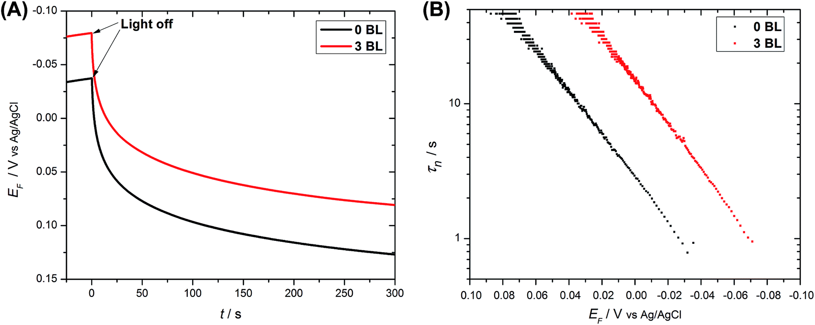 | ||
| Fig. 6 Open-circuit voltage decays for DSPECs with and without compact layers. (A) EF–time decay and (B) electron lifetime as a function of EF (20 mmol L−1 acetate buffer, pH 4.6, 0.50 mol L−1 LiClO4vs. Ag/AgCl). | ||
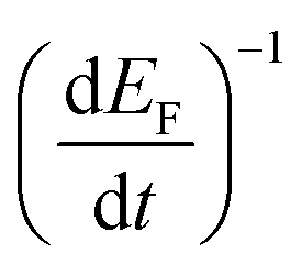
Electron lifetimes (τn) – a recovery time when the system is displaced from open circuit condition, dictated by eqn (2) – vary logarithmically with open circuit potential, for both cases, Fig. 6(B).
 | (2) |
 , accounting for thermal energy involved during Fermi level equilibration.33–35 A longer electron lifetime was observed for a 3 BL DSPEC, because of a higher electron density (n), eqn (3),22,33 since the recombination term (U(n)) is negligible for DSPECs
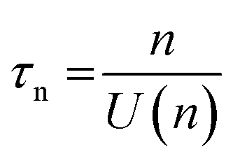 | (3) |
The role of a 3 BL compact TiO2 film is mostly due to the improved physical contact between the mesoporous network and FTO, that resulted in a 53% photocurrent enhancement for 3 BL DSPEC. The compact films are acting as contact layers22,23,25 providing efficient electron collection as corroborated by IPCE enhancements.
Conclusion
The use of compact TiO2 bilayers beneath a nanoITO/TiO2 core/shell assembly provides an enhanced physical contact with FTO and impressive photocurrent improvements of 53%. Complementary photoelectrochemical measurements also demonstrated enhanced electron lifetimes. There is also a shift to more negative potentials that may favor O2 evolution at the photoanode with an additional significant impact on DSPEC performance. Introduction of this innovative, low-cost approach into DSPEC designs may well open up new possibilities for water-splitting device improvements.Acknowledgements
R. L. C. and N. Y. M. I. are supported by Fundação de Amparo à Pesquisa do Estado de São Paulo (FAPESP) and Conselho Nacional de Desenvolvimento Científico e Tecnológico (CNPq). The authors also thank Chapel Hill Analytical and Nanofabrication Laboratory (CHANL) for ALD and ellipsometry facilities, Dr Amar S. Kumbhar, for microscopy images and EDS, and Dr Kassio P. S. Zanoni, Dr Christopher J. Dares, and Dr Matthew V. Sheridan, for general assistance.References
- L. Alibabaei, H. Luo, R. L. House, P. G. Hoertz, R. Lopez and T. J. Meyer, J. Mater. Chem. A, 2013, 1, 4133–4145 CAS.
- R. L. House, N. Y. Murakami Iha, R. L. Coppo, L. Alibabaei, B. D. Sherman, P. Kang, M. K. Brennaman, P. G. Hoertz and T. J. Meyer, J. Photochem. Photobiol., C, 2015, 25, 32–45 CrossRef CAS.
- B. O'Regan and M. Grätzel, Nature, 1991, 353, 737–740 CrossRef.
- M. K. Nazeeruddin, A. Kay, I. Rodicio, R. Humphry-Baker, E. Müller, P. Liska, N. Vlachopoulos and M. Gratzel, J. Am. Chem. Soc., 1993, 115, 6382–6390 CrossRef CAS.
- C. G. Garcia, J. F. de Lima and N. Y. Murakami Iha, Coord. Chem. Rev., 2000, 196, 219–247 CrossRef CAS.
- C. G. Garcia and N. Y. Murakami Iha, Int. J. Photoenergy, 2001, 3, 131–135 CrossRef CAS.
- A. S. Polo, M. K. Itokazu and N. Y. Murakami Iha, Coord. Chem. Rev., 2004, 248, 1343–1361 CrossRef CAS.
- M. Grätzel, Inorg. Chem., 2005, 44, 6841–6851 CrossRef PubMed.
- S. Mathew, A. Yella, P. Gao, R. Humphry-Baker, B. F. E. Curchod, N. Ashari-Astani, I. Tavernelli, U. Rothlisberger, M. K. Nazeeruddin and M. Grätzel, Nat. Chem., 2014, 6, 242–247 CrossRef CAS PubMed.
- J. J. Concepcion, J. W. Jurss, M. K. Brennaman, P. G. Hoertz, A. O. T. Patrocinio, N. Y. Murakami Iha, J. L. Templeton and T. J. Meyer, Acc. Chem. Res., 2009, 42, 1954–1965 CrossRef CAS PubMed.
- M. V. Sheridan, B. D. Sherman, R. L. Coppo, D. Wang, S. L. Marquard, K.-R. Wee, N. Y. Murakami Iha and T. J. Meyer, ACS Energy Lett., 2016, 1, 231–236 CrossRef CAS.
- L. Alibabaei, M. K. Brennaman, M. R. Norris, B. Kalanyan, W. Song, M. D. Losego, J. J. Concepcion, R. A. Binstead, G. N. Parsons and T. J. Meyer, Proc. Natl. Acad. Sci. U. S. A., 2013, 110, 20008–20013 CrossRef CAS PubMed.
- L. Alibabaei, B. D. Sherman, M. R. Norris, M. K. Brennaman and T. J. Meyer, Proc. Natl. Acad. Sci. U. S. A., 2015, 112, 5899–5902 CrossRef CAS PubMed.
- L. Alibabaei, B. H. Farnum, B. Kalanyan, M. K. Brennaman, M. D. Losego, G. N. Parsons and T. J. Meyer, Nano Lett., 2014, 14, 3255–3261 CrossRef CAS PubMed.
- B. Peng, G. Jungmann, C. Jäger, D. Haarer, H.-W. Schmidt and M. Thelakkat, Coord. Chem. Rev., 2004, 248, 1479–1489 CrossRef CAS.
- J. N. Hart, D. Menzies, Y.-B. Cheng, G. P. Simon and L. Spiccia, J. Sol-Gel Sci. Technol., 2006, 40, 45–54 CrossRef CAS.
- P. Lellig, M. A. Niedermeier, M. Rawolle, M. Meister, F. Laquai, P. Müller-Buschbaum and J. S. Gutmann, Phys. Chem. Chem. Phys., 2012, 14, 1607–1613 RSC.
- S. S. Huang and J. S. Chen, J. Mater. Sci.: Mater. Electron., 2002, 13, 77–81 CrossRef CAS.
- M. J. Alam and D. C. Cameron, J. Mater. Sci., 2001, 36, 5923–5926 CrossRef.
- D. H. Kim, M. Woodroof, K. Lee and G. N. Parsons, ChemSusChem, 2013, 6, 1014–1020 CrossRef CAS PubMed.
- R. S. Pessoa, M. A. Fraga, L. V. Santos, M. Massi and H. S. Maciel, Mater. Sci. Semicond. Process., 2015, 29, 56–68 CrossRef CAS.
- K. P. S. Zanoni, R. C. Amaral and N. Y. Murakami Iha, ACS Appl. Mater. Interfaces, 2014, 6, 10421–10428 CAS.
- A. O. T. Patrocinio, A. S. El-Bachá, E. B. Paniago, R. M. Paniago and N. Y. Murakami Iha, Int. J. Photoenergy, 2012, 2012, 1–7 CrossRef.
- A. O. T. Patrocínio, L. G. Paterno and N. Y. Murakami Iha, J. Photochem. Photobiol., A, 2009, 205, 23–27 CrossRef.
- A. O. T. Patrocinio, L. G. Paterno and N. Y. Murakami Iha, J. Phys. Chem. C, 2010, 114, 17954–17959 CAS.
- L. F. Paula, R. C. Amaral, N. Y. Murakami Iha, R. M. Paniago, A. E. H. Machado and A. O. T. Patrocinio, RSC Adv., 2014, 4, 10310–10316 RSC.
- J. W. Ostrander, A. A. Mamedov and N. A. Kotov, J. Am. Chem. Soc., 2001, 123, 1101–1110 CrossRef CAS PubMed.
- J. R. Swierk, N. S. McCool, T. P. Saunders, G. D. Barber and T. E. Mallouk, J. Am. Chem. Soc., 2014, 10974–10982 CrossRef CAS PubMed.
- M. R. Norris, J. J. Concepcion, Z. Fang, J. L. Templeton and T. J. Meyer, Angew. Chem., Int. Ed., 2013, 52, 13580–135803 CrossRef CAS PubMed.
- A. J. Frank, N. Kopidakis and J. van de Lagemaat, Coord. Chem. Rev., 2004, 248, 1165–1179 CrossRef CAS.
- Z. Chen, H. N. Dinh and E. Miller, Photoelectrochemical water splitting: standards, experimental methods, and protocols, Springer, London, UK, 1st edn, 2013 Search PubMed.
- H. Li, Z. Chen, C. K. Tsang, Z. Li, X. Ran, C. Lee, B. Nie, L. Zheng, T. Hung, J. Lu, B. Pan and Y. Y. Li, J. Mater. Chem. A, 2014, 2, 229–236 CAS.
- A. Zaban, M. Greenshtein and J. Bisquert, ChemPhysChem, 2003, 4, 859–864 CrossRef CAS PubMed.
- J. Bisquert, J. Phys. Chem. B, 2002, 106, 325–333 CrossRef CAS.
- T. Berger, D. Monllor-Satoca, M. Jankulovska, T. Lana-Villarreal and R. Gómez, ChemPhysChem, 2012, 13, 2824–2875 CrossRef CAS PubMed.
Footnote |
| † Electronic supplementary information (ESI) available: EDS spectrum for compact TiO2, J–t curves with three cycles of turn on/turn off irradiation for DSPECs, and UV-Vis spectrum of the photoanode with 3 BL. See DOI: 10.1039/c6se00022c |
| This journal is © The Royal Society of Chemistry 2017 |