 Open Access Article
Micrometre and nanometre scale patterning of binary polymer brushes, supported lipid bilayers and proteins†
Alexander
Johnson
a,
Jeppe
Madsen
 a,
Paul
Chapman
ab,
Abdullah
Alswieleh
a,
Omed
Al-Jaf
a,
Peng
Bao
c,
Claire R.
Hurley
a,
Michaël L.
Cartron
d,
Stephen D.
Evans
c,
Jamie K.
Hobbs
be,
C. Neil
Hunter
a,
Paul
Chapman
ab,
Abdullah
Alswieleh
a,
Omed
Al-Jaf
a,
Peng
Bao
c,
Claire R.
Hurley
a,
Michaël L.
Cartron
d,
Stephen D.
Evans
c,
Jamie K.
Hobbs
be,
C. Neil
Hunter
 d,
Steven P.
Armes
 a and
Graham J.
Leggett
 *ae
*ae
aDepartment of Chemistry, University of Sheffield, Brook Hill, Sheffield S3 7HF, UK. E-mail: graham.leggett@sheffield.ac.uk
bDepartment of Physics and Astronomy, University of Sheffield, Sheffield S3 7RH, UK
cMolecular and Nanoscale Physics Group, School of Physics and Astronomy, University of Leeds, Leeds LS2 9JT, UK
dDepartment of Molecular Biology and Biotechnology, University of Sheffield, Western Bank, Sheffield S10 2TN, UK
eKrebs Institute, University of Sheffield, Sheffield, South Yorkshire S10 2TN, UK
First published on 18th April 2017
Abstract
Binary polymer brush patterns were fabricated via photodeprotection of an aminosilane with a photo-cleavable nitrophenyl protecting group. UV exposure of the silane film through a mask yields micrometre-scale amine-terminated regions that can be derivatised to incorporate a bromine initiator to facilitate polymer brush growth via atom transfer radical polymerisation (ATRP). Atomic force microscopy (AFM) and imaging secondary ion mass spectrometry (SIMS) confirm that relatively thick brushes can be grown with high spatial confinement. Nanometre-scale patterns were formed by using a Lloyd's mirror interferometer to expose the nitrophenyl-protected aminosilane film. In exposed regions, protein-resistant poly(oligo(ethylene glycol)methyl ether methacrylate) (POEGMEMA) brushes were grown by ATRP and used to define channels as narrow as 141 nm into which proteins could be adsorbed. The contrast in the pattern can be inverted by (i) a simple blocking reaction after UV exposure, (ii) a second deprotection step to expose previously intact protecting groups, and (iii) subsequent brush growth via surface ATRP. Alternatively, two-component brush patterns can be formed. Exposure of a nitrophenyl-protected aminosilane layer either through a mask or to an interferogram, enables growth of an initial POEGMEMA brush. Subsequent UV exposure of the previously intact regions allows attachment of ATRP initiator sites and growth of a second poly(cysteine methacrylate) (PCysMA) brush within photolithographically-defined micrometre or nanometre scale regions. POEGMEMA brushes resist deposition of liposomes, but fluorescence recovery after photobleaching (FRAP) studies confirm that liposomes readily rupture on PCysMA “corrals” defined within POEGMEMA “walls”. This leads to the formation of highly mobile supported lipid bilayers that exhibit similar diffusion coefficients to lipid bilayers formed on surfaces such as glass.
Introduction
Polymer brushes1 have attracted widespread interest for the control of interfacial phenomena ranging from lubrication2–6 to biological fouling.7–9 Brush layers may be formed by grafting preformed polymer chains onto a surface, or by growing polymers from surfaces using surface-initiated polymerisation. Among the latter class of methods, atom transfer radical polymerisation (ATRP)10,11 has proved to be a powerful tool, offering the means to grow dense, relatively thick brushes with good control. There has been much interest in the use of polymer brushes to fabricate devices such as sensors.12 Brushes can be designed to be stimulus-responsive,13,14 and many brushes are known to be highly resistant to biological fouling.7–9,15–19 For example, poly(oligo(ethylene glycol)ether methacrylate) (POEGMEMA)9 and poly(2-(methacryloyloxy)ethyl phosphorylcholine) (PMPC)15–17 offer exceptional resistance to the adsorption of biological molecules. In this context, we have demonstrated that pH-responsive brushes comprising poly(cysteine methacrylate) (PCysMA) grown by ATRP confer exceptional biocompatibility and resistance to fouling to planar substrates.19 Although not commercially available, the CysMA monomer is readily synthesized on a forty-gram scale in water at ambient temperature using cheap precursors, while PCysMA brush growth is both rapid and well-controlled when conducted in aqueous solution.In many putative applications of brushes, the ability to form patterns is required. For example, spatially-controlled protein adsorption may be essential for a biological diagnostic device. One approach to the formation of a patterned polymer brush is to pattern an initiator and then use surface-initiated polymerisation to grow polymers from initiator-functionalised regions.20 A wide range of methods has been used to form patterns of initiator, including microcontact printing,20–22 photopatterning,23–27 nanoimprint lithography,28 scanning probe methods13,29–31 and electron beam lithography.32–36 Alternatively, an initiator-functionalised surface can be activated in a spatially selective fashion. For example, Prucker et al. grew patterned polymer brushes from a surface functionalised with a photo-initiator by using photolithography to expose selected areas of the surface.37 Gradient structures, consisting of brush layers with controlled spatial variation in density, can be prepared by controlling the exposure when using either electron-beam lithography38 or photolithography.26,27,39 Alternatively, the controlled immersion of a substrate into a solution of a polymer.40 Alternatively, a pre-formed polymer layer may be fabricated and then modified, for example by electron beam lithography.41
However, methods for the spatial organisation of two contrasting brushes at a planar surface – potentially vital in the design of many types of functional device – are less well developed, particularly for nanopatterned brushes. Perhaps the simplest approach is to exploit phase separation in copolymer blends formed from immiscible polymers,42 but for top-down control of architecture, lithographic processing is required.
One strategy for the fabrication of binary brushes is to adapt conventional photolithography, using an initial UV exposure and development protocol to pattern and grow one brush, and then removing residual photoresist to enable growth of a second brush.43 However, development of the photoresist places some constraints on this approach. Prucker et al. used photolithography to form features in polystyrene films, into which a brush could then be grown to yield a two-component pattern.37 Another approach is to form a continuous brush layer, which is then end-capped by reaction with an azide.44,45 Exposure to UV light enables functionalization of selected regions of the surface with initiator sites, facilitating growth of a second brush.44 Alternatively, the azide can be converted to an amine protected by a photocleavable group, allowing subsequent patterning.45 Huck and co-workers described an approach based on micro-contact printing, in which a thiol-functional initiator is patterned onto a planar surface.21 After brush growth, the initiator at the growing polymer chain-end is deactivated and a second patterning step is used to deposit initiator-terminated adsorbates in fresh regions of the surface to facilitate growth of a chemically distinct second brush layer.
For nano-scale patterned brushes, the technical problems are considerably more challenging. Hu et al. described an approach based on colloidal templating, in which an initial polymer forms a film on a substrate on which a close-packed array of colloidal particles has been formed.46 Subsequently, the colloidal particles are removed and the resulting vacancies are filled with a second polymer. A scanning probe approach has been described by Chen et al.,47 who formed a continuous planar brush layer and then used an array of cantilever probes to deposit initiator by pushing the probes through the brush layer until they contacted the substrate. A subsequent polymerisation step yielded nanoscale brush structures.
In this paper we describe a simple, new approach to the fabrication of binary brush structures that is applicable across multiple length scales, from microns to nanometres, and is compatible with inexpensive large-area processing. Aminosilane films are commonly used in ATRP; they may be brominated readily by amidation using 2-bromoisobutyryl bromide to facilitate subsequent brush growth. We reported recently that N-[2-(2-nitrophenyl)propan-1-oxycarbonyl] (NPPOC) groups can be used as photocleavable protecting groups for aminosilanes.48 Exposure of the protected film to near-UV light leads to selective removal of the NPPOC group (Scheme 1), enabling derivatisation of free amines.48,49 This enables spatial control of surface reactivity to be achieved at the micrometre scale using a mask, or at much shorter length scales using a near-field probe.48,49 In the present study, we apply this strategy to the fabrication of binary polymer brushes, using a mask-based process to fabricate micrometre-scale structures and interferometric exposure to achieve high-fidelity patterning across macroscopic areas with nanometre scale resolution.
In principle, patterned supported lipid bilayers (SLBs) enable investigation of dynamical processes such as membrane signalling50–52 and electrophoresis.53–57 Thus an important overarching objective of the present study was to develop robust methods for the 2D confinement of SLBs. Recently, PCysMA has emerged as a very promising candidate brush for such work.58 It is a non-fouling brush19 that enables the selective adsorption and rupture of liposomes to form SLBs that contain highly mobile lipids.58 The specific aim of the present study was to develop methods for the fabrication of PCysMA “corrals” within “walls” formed from a non-fouling brush, with the “corrals” enabling the construction of spatially-confined highly mobile SLBs. The data presented here demonstrate that judicious photopatterning combined with the use of nitrophenyl protecting groups and surface ATRP provides a convenient and effective means to produce well-defined binary brush structures.
Results and discussion
Film formation and characterisation
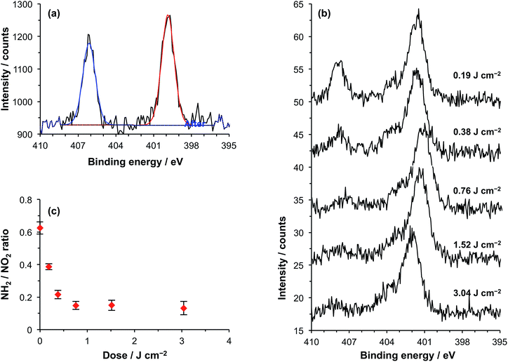
NPPOC-APTES is a nitrophenyl-protected aminopropyltriethoxysilane that forms smooth, covalently-anchored thin films on oxide surfaces.48 UV exposure causes elimination of the NPPOC group to yield the free primary amine (Scheme 1). NPPOC-APTES films were prepared on silicon oxide according to previously published methodology. The water contact angle of the virgin films was 68 ± 1°, which is similar to the value reported previously.48 A surface roughness (RMS) of 0.4 nm was determined by AFM, confirming the formation of smooth films.Fig. 1a shows the high-resolution N 1s spectrum of a virgin NPPOC-APTES film. Two bands are evident at 400.0 eV and 406.1 eV corresponding to the chemically distinct nitrogen atoms in the carbamate and nitro groups, respectively.
On UV irradiation of a NPPOC-APTES film at 244 nm, the intensity of the nitro component in the N 1s region was reduced significantly after a 1.5 J cm−2 dose (Fig. 1b). This indicates deprotection of the amine group, leading to loss of the nitrophenyl moiety from the surface. The binding energy of the carbamate nitrogen atom is very close to that of a nitrogen atom in an amine. In fact, these two environments are closer in energy than the spectrometer resolution and hence cannot be resolved.
Fig. 1c shows the variation in the ratio of the intensities of the components observed at 406.1 eV and 400.0 eV as a function of UV dose. As the dose increases, this ratio decreases. As photodeprotection increases, the component at 400.0 eV most likely results increasingly from photoemission from an amine (rather than a carbamate) nitrogen species.48 This ratio reaches a limiting value at an exposure of ∼0.75 J cm−2. As far as we are aware, photodeprotection of NPPOC-APTES has not been studied at 244 nm previously. Alang-Ahmad et al. studied the behaviour after exposure at 325 nm,48 and reported that the NO2![[thin space (1/6-em)]](https://www.rsc.org/images/entities/char_2009.gif) :
:![[thin space (1/6-em)]](https://www.rsc.org/images/entities/char_2009.gif) NH2 intensity ratio reached a limiting value after a dose of ∼3 J cm−2, so the data shown in Fig. 1c suggest that deprotection is around four times faster for the more energetic photons used here.
NH2 intensity ratio reached a limiting value after a dose of ∼3 J cm−2, so the data shown in Fig. 1c suggest that deprotection is around four times faster for the more energetic photons used here.
Fabrication of polymer brush patterns
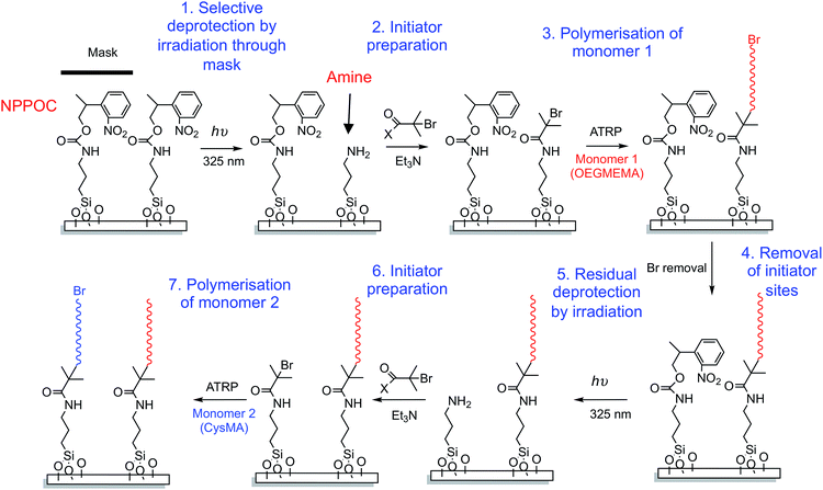
A reaction scheme for the fabrication of binary patterned polymer brushes is shown in Scheme 2. A mask is placed over a NPPOC-APTES functionalised wafer and subsequent UV irradiation (244 nm) leads to deprotection of amine groups in exposed regions. This surface-patterned wafer is then immersed in a BIBB solution, leading to installation of ATRP initiator sites in the exposed regions. Surface ATRP is conducted to produce the desired patterned polymer brush. The surface is then reacted with sodium azide to end-cap the first polymer brush, and exposed to near UV light (325 nm, not damaging to the first brush) to deprotect the remaining NPPOC-APTES adsorbates. These regions are functionalised with an initiator, enabling growth of the second brush by ATRP.It is important to note that if strictly anhydrous BIBB is used to derivatise the patterned regions with initiators, a side-reaction can occur between the BIBB and the carbamate group of NPPOC-APTES, leading to the introduction of Br in regions that were not exposed to UV light. A detailed analysis of this side-reaction is provided in the ESI.† To prevent this side-reaction, a sub-stoichiometric amount of water should be present in the BIBB solution. Under such conditions, which were only identified by serendipity, only the regions of the sample that have been exposed to UV light are derivatized by the BIBB reagent.
Single component brush patterns were fabricated first (steps 1–3 in Scheme 2), and characterised by secondary ion mass spectrometry (SIMS). SIMS imaging is a powerful tool for the characterisation of patterned surfaces: it provides high molecular specificity and can be used to determine the spatial distribution of chemical fragments with high sensitivity.59 Here, SIMS imaging was used to assess the extent of polymer growth from defects in masked regions (i.e.) sites where adventitious removal of the protecting group might have occurred.
Negative ion SIMS spectra of POEGMEMA are dominated by peaks assigned to small carbon–oxygen clusters, that are observed at low intensity in spectra of other materials. In order to eliminate any possibility for ambiguity, poly(2-(methacryloyloxy)ethyl phosphorylcholine) (PMPC) brushes were grown from patterned samples for SIMS analysis, rather than POEGMEMA brushes. PMPC yields unambiguous peaks corresponding to phosphorus-containing ions at m/z 62.97 (PO2−) and m/z 78.97 (PO3−) that are not expected to be observed in the SIMS spectra of any other materials used in this study. SIMS spectra of intact NPPOC-APTES films yielded peaks corresponding to CN− (m/z 26.02), CNO− (m/z 42.02) and NO2− (m/z 46.01).
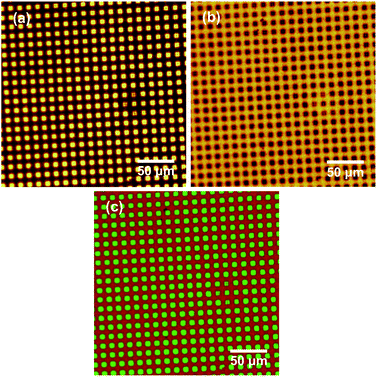
SIMS was used to image a micrometre-patterned PMPC brush. A complete spectrum was recorded for each pixel, enabling the distributions of anions of interest to be compared. Fig. 2a shows an image of the sum of the intensities corresponding to the PO2− and PO3− ions in the negative ion SIMS spectrum. Bright contrast is observed in regions exposed to UV radiation during photopatterning (squares). The photocleavable protecting group was removed in these regions, and PMPC brushes were subsequently grown from these locations via surface ATRP. However, dark contrast is observed for areas (bars) that were masked during UV exposure, indicating that the protecting group has remained intact, hence no brushes could be grown from these regions. It is perhaps worth emphasising here that ATRP is an unforgiving surface functionalization step: a single Br initiator defect leads to the introduction of a significant amount of undesired material because each polymer chain comprises up to hundreds of monomer repeat units. The substantial contrast difference observed between the masked and exposed areas shown in Fig. 2a thus indicates that adventitious deprotection of the masked surface regions is negligible.
Fig. 2b shows an image formed by summing the intensities of the CN−, CNO− and NO2− ions. As expected, bright contrast is observed for the masked regions (bars), while dark contrast is obtained in the exposed regions. Fig. 2c shows a false-colour image produced by superimposing a map of the NO2− intensity (red) on that of the PO2− and PO3− intensity (green) assigned to the PMPC chains. Clearly, spatial confinement of both photodeprotection and brush growth can be achieved with excellent precision.
Inverting the tone of the resist
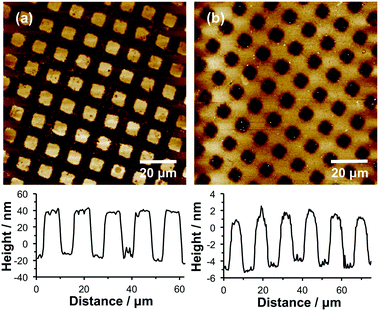
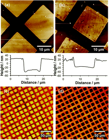
During fabrication of the pattern shown in Fig. 2, NPPOC-APTES acts as a positive tone resist (i.e. the protecting group was removed during UV exposure, enabling subsequent brush growth from such regions). Alternatively, inverted contrast can be achieved after initial photodeprotection by treating the substrate with trifluoroacetic anhydride (TFAA). This reagent reacts with amine groups to form amides that are unreactive towards BIBB, hence brushes cannot grow from the exposed regions. The remaining unexposed regions can then be deprotected by irradiating the whole wafer at 325 nm, enabling subsequent reaction with BIBB and growth of polymer brushes via surface ATRP. Thus this strategy enables NPPOC-APTES to be utilised as a negative tone resist.Fig. 3 shows tapping mode AFM topographical images obtained for two POEGMEMA patterns produced with and without this blocking step. In Fig. 3a, the POEGMEMA brushes were grown from UV-exposed regions (squares) while the masked regions (bars) should contain no polymer chains. Fig. 3b shows a patterned wafer formed by first blocking the initial UV-exposed square regions by reaction with TFAA. The second exposure at 325 nm deprotected the bars, which were masked during the first exposure, enabling their functionalisation with ATRP initiator to facilitate brush growth.
Interferometric lithography
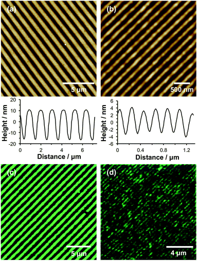
Nanostructured brushes were fabricated using interferometric lithography (IL). In this case, photodeprotection was achieved by exposing substrates to an interferogram formed using a Lloyd's mirror two-beam interferometer. At locations in which the sample was exposed to a maximum in the interferogram, the adsorbate was deprotected, enabling attachment of Br initiator molecules and the subsequent growth of polymer brushes by surface ATRP. As a result, linear brush nanostructures were formed. By controlling the angle between the sample and the mirror in the interferometer, the pitch of the nanostructures could be controlled. Fig. 4 shows tapping mode topographical AFM images of POEGMEMA nanopatterned brushes formed using an exposure of 2.70 J cm−1 and angles of 5° (a) and 35° (b). The pitches of these structures are 1.10 μm and 206 nm, respectively, while the full widths at half maximum (FWHM) of these features are 404 nm and 83 nm, respectively. The heights of the narrower features (Fig. 4b) are significantly less than the heights of the features formed with a larger pitch (Fig. 4a). This is attributed to the significantly greater lateral freedom of the grafted chains in nanostructured brushes.34,60It is well-documented that POEGMEMA brushes strongly resist the adsorption of biomolecules on surfaces.7,8 Thus the anti-biofouling performance of POEGMEMA nanostructured brushes was evaluated by immersing such wafers in an aqueous solution of green fluorescent protein (GFP) at 20 °C, followed by imaging using confocal fluorescence microscopy. Fig. 4c and d show images acquired for two samples for which the mean widths of the brush-free channels were 656 nm and 141 nm, respectively. Clearly, the fluorescence intensity is localised within well-defined lines, thus demonstrating the selective adsorption of GFP onto the NPPOC-APTES regions of the pattern. In Fig. 4d, the channel width is smaller than the diffraction limit; the observed feature sizes are most likely determined by the point-spread function of the optical system. Thus, although smaller structures were fabricated, it was not possible to resolve the features because of the intrinsic limitations of conventional optical microscopy. Nevertheless, there is no intrinsic reason why even finer protein patterns could not be formed using the nanopatterning strategy described herein. Such structures would require the utilisation of super-resolution microscopy techniques, e.g. STORM61 or PALM62 for characterisation studies.
Fabrication of binary brush structures
An initial single-brush pattern was first fabricated as described above (steps 1–3, Scheme 2). In principle, each grafted polymer chain should have a terminal Br atom. In practice, there is likely to be less than one Br atom per chain, because ATRP is only a pseudo-living radical polymerisation. All living chain-ends must be terminated with a non-living functional group if a second, chemically distinct polymer brush is to be grown from the surface. This was achieved by reacting the brush chain-ends with sodium azide, as described previously (step 4, Scheme 2).21,45 This leads to replacement of each Br atom with an azide. The entire surface is then exposed to UV radiation at 325 nm (step 5), leading to removal of the remaining NPPOC protecting groups to generate surface amine sites. These are then amidated using excess BIBB to yield Br initiator sites (step 6) from which a second polymer brush is grown via surface ATRP (step 7). Our goal was to form “corrals” that enclosed supported lipid bilayers for studies of membrane diffusion processes. Thus a zwitterionic polymer, poly(cysteine methacrylate), PCysMA, was selected as the second brush. PCysMA chains may be grown in a well-controlled fashion from planar surfaces to yield stimulus-responsive, protein-resistant biocompatible brush layers19 that enable the facile construction of supported lipid bilayers (SLBs).58 Because the goal was to fabricate enclosures (or “corrals”) for SLBs, the PCysMA brush thickness was selected to be less than that of the initial non-ionic POEGMEMA brush.Fig. 5a shows an AFM topographical image of a brush structure formed by exposing an NPPOC-APTES film to UV radiation through a 600 mesh copper grid. The deprotected amine groups were reacted with BIBB to produce a brominated surface from which POEGMEMA brushes were subsequently grown. From the line section, the height difference between the masked and exposed regions was found to be 54 nm after surface ATRP. The POEGMEMA brush chain-ends were then azide-capped and the wafer was irradiated at 325 nm to remove the remaining NPPOC groups, which enabled PCysMA brushes to be grown from these regions. The height difference between the square and the bar region of the pattern was reduced to 33 nm (Fig. 5b), indicating the formation of a PCysMA brush with a mean thickness of 21 nm. SIMS imaging provided further evidence for the presence of two chemically distinct, spatially-organised brushes within the pattern. For PCysMA, CN− (m/z 26), S− (m/z 32.07), HS− (m/z 33.07) C2HS− (m/z 57.09), C4HS− (m/z 81.12) and C3H5SO2− (m/z 105.12) were identified as characteristic anions in the negative ion SIMS spectra. For POEGMEMA, the characteristic anions were determined to be C2H3O− (m/z 43.04), C2H2O2− (m/z 58.04) and C4H5O2− (m/z 85.08). Fig. 6c shows a SIMS image formed by mapping the summed intensities of the ions that are characteristic of POEGMEMA, while Fig. 5d shows a SIMS image of the summed intensities of the PCysMA-specific ions. Comparison of these images confirms that each brush has been grown from precise surface regions on the patterned substrate: POEGMEMA chains have grown exclusively from the square regions exposed in the first stage of the patterning process, whereas PCysMA chains have grown from the remainder of the surface.
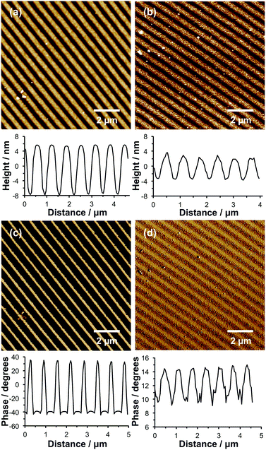
Using IL, the same methodology can also be used to fabricate nanostructured binary brushes. First, nanolines were formed by UV exposure of NPPOC-APTES films using a Lloyd's mirror interferometer, functionalization of the deprotected amines with Br and finally surface ATRP of OEGMEMA. Fig. 6a shows a tapping mode topographical AFM image of the resulting patterned brush. The structures have a FWHM of 247 nm, and a mean peak-to-trough height of 12.8 nm. As noted above, nanostructured brushes typically exhibit significantly lower heights compared to uniform (i.e. non-patterned) brushes formed under identical conditions.60 Moreover, height measurements were performed on dry brushes because the low moduli of solvent-swollen brushes make such studies technically challenging if reliable quantitative data are required.
The entire wafer was then exposed to UV radiation at 325 nm, leading to deprotection of all remaining APTES adsorbates, and the resulting surface amine groups were amidated to introduce Br initiator sites. PCysMA brushes were then grown from the channels between the nanostructured POEGMEMA brushes. A reduction in the apparent POEGMEMA brush height to 5.6 nm was observed (Fig. 6b), indicating the growth of a PCysMA brush layer with a mean thickness of 7.2 nm.
Unfortunately, imaging SIMS does not have sufficient resolution to confirm the formation of these binary brush nanostructures. Instead, AFM phase imaging was used to provide support for the formation of distinct surface regions occupied by the POEGMEMA and PCysMA brushes. In phase imaging, the phase lag between the driving oscillation applied to a cantilever in tapping mode and the cantilever response is measured; for viscous surfaces, there is a high rate of energy dissipation leading to a significant phase lag, but for elastic materials the phase lag is small. Thus, changes in the phase signal can be used to provide a qualitative map of chemically distinct surface regions.
Fig. 6c and d show AFM phase images recorded for POEGMEMA nanolines before and after PCysMA brush growth. In the absence of PCysMA, the phase difference between the POEGMEMA and NPPOC-APTES regions of the patterns was large (68.2°). This can be explained by the differing mechanical properties between the two regions of the pattern: the brush regions should have a small elastic modulus, and hence yield a high rate of energy dissipation, while the intervening regions, which are covered only with a thin film of NPPOC-APTES, are expected to yield a much lower rate of energy dissipation. The image shown in Fig. 6c was acquired simultaneously with that in Fig. 6a; comparison of the two suggests that the narrow bands of bright contrast in Fig. 6c correspond to the narrow regions evident in the line section through Fig. 7a where the POEGMEMA is entirely absent. Because IL yields a gradient of UV exposure, this creates a corresponding structural gradient from regions where the surface has been completely deprotected (maxima in the line section through Fig. 6a) and regions were there are no brushes (minima). Moreover, the comparatively high degree of freedom of nanostructured brushes means that there is some lateral “spread” in the surface-grafted POEGMEMA chains. However, after growth of the PCysMA brush, the phase contrast between the different regions is dramatically reduced to just 4.8°. This much lower phase contrast indicates that the entire surface is now covered with surface-grafted polymer chains, so that the rate of energy dissipation during tapping is relatively uniform.
Formation of supported lipid bilayers
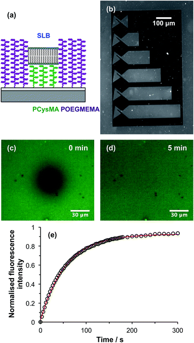
These binary brush structures were used to enclose SLBs. We have previously demonstrated that highly mobile SLBs can be formed on PCysMA brushes, but not on POEGMEMA brushes.58 In the present work, binary brush patterns were designed in which PCysMA brushes are enclosed within “walls” fabricated from POEGMEMA brushes (Fig. 7a). A low-magnification fluorescence microscopy image is shown in Fig. 7b of a structure consisting of six direct current (dc) traps of varying lengths fabricated from PCysMA brushes. These structures were designed for studies of electrophoresis in supported lipid bilayers after the work of Roth et al.57 In these traps, dye-labelled lipids accumulate in structures at the left-hand ends, giving rise to an increase in fluorescence. An SLB has been formed in the trap regions by rupture of vesicles containing a small concentration of a fluorescent dye. After initial UV exposure of an NPPOC-APTES film, during which the trap regions were masked, the walls (dark regions) were defined by surface ATRP of OEGMEMA. This patterned wafer was then exposed to UV radiation at 325 nm and a PCysMA brush was grown from the trap regions. The conditions used for this polymerisation of CysMA were controlled to ensure that the POEGMEMA “walls” were always higher than the PCysMA “trap” regions, as shown in Fig. 5b and 6b.Ternary lipid bilayers (DOPC![[thin space (1/6-em)]](https://www.rsc.org/images/entities/char_2009.gif) :
:![[thin space (1/6-em)]](https://www.rsc.org/images/entities/char_2009.gif) DOTAP
DOTAP![[thin space (1/6-em)]](https://www.rsc.org/images/entities/char_2009.gif) :
:![[thin space (1/6-em)]](https://www.rsc.org/images/entities/char_2009.gif) NBD–DHPE = 74
NBD–DHPE = 74![[thin space (1/6-em)]](https://www.rsc.org/images/entities/char_2009.gif) :
:![[thin space (1/6-em)]](https://www.rsc.org/images/entities/char_2009.gif) 25
25![[thin space (1/6-em)]](https://www.rsc.org/images/entities/char_2009.gif) :
:![[thin space (1/6-em)]](https://www.rsc.org/images/entities/char_2009.gif) 1) were formed on PCysMA brushes using the method described in the Experimental section. Because the bilayer contained 1 mol% NBD–DHPE (a green fluorescent dye), it was possible to evaluate the efficiency of containment of the bilayers by fluorescence microscopy (Fig. 7b). Clearly, fluorescence is observed only within the trap structures. Moreover, the surrounding POEGMEMA regions remain dark, indicating that liposome adsorption is negligible on these non-fouling brushes. Thus the POEGMEMA “walls” confine SLB formation to the PCysMA regions defined in the initial UV exposure.
1) were formed on PCysMA brushes using the method described in the Experimental section. Because the bilayer contained 1 mol% NBD–DHPE (a green fluorescent dye), it was possible to evaluate the efficiency of containment of the bilayers by fluorescence microscopy (Fig. 7b). Clearly, fluorescence is observed only within the trap structures. Moreover, the surrounding POEGMEMA regions remain dark, indicating that liposome adsorption is negligible on these non-fouling brushes. Thus the POEGMEMA “walls” confine SLB formation to the PCysMA regions defined in the initial UV exposure.
To determine whether the lipids within the SLB confined within the trap regions remained mobile, fluorescence recovery after photobleaching (FRAP) experiments were performed. Fig. 7c shows a fluorescence micrograph recorded for an SLB supported on PCysMA brushes within one of the trap structures shown in Fig. 7b immediately after photobleaching. Fig. 7d shows the same region 5 min after photobleaching: the dark spot has disappeared, and the fluorescence has become uniform again. This provides qualitative evidence that the lipids within the SLB are mobile. Fig. 7e shows this fluorescence recovery as a function of time. The data have been fitted (red curve in Fig. 7e). Analysis of the recovery curve using the Axelrod method63 yields a mobile fraction of 93% and a diffusion coefficient of 1.36 μm2 s−1, which are comparable to literature values determined for the same lipids on positive control surfaces such as glass.58 These data provide strong evidence that the PCysMA “corrals” formed within POEGMEMA “walls” enable the construction of spatially-confined, highly mobile SLBs.
Conclusions
Photopatterning of NPPOC-APTES films provides a facile and versatile route to the fabrication of well-defined two-component brush structures. Exposure of NPPOC-APTES through a mask enables the fabrication of micrometre-scale patterns of amines, which enables convenient attachment of initiator sites for brush growth via atom transfer radical polymerisation. Analysis by atomic force microscopy and imaging secondary ion mass spectrometry confirms that non-ionic POEGMEMA brushes are produced with high fidelity. Nanometre-scale initiator structures can be fabricated using a Lloyd's mirror interferometer in place of a mask during UV exposure. Surface ATRP of POEGMEMA produces nanopatterned brushes that enable formation of high-fidelity protein nanopatterns with negligible non-specific adsorption on brush regions. Alternatively, a second brush component can be introduced via UV irradiation of NPPOC-APTES groups that remained intact after the first UV exposure. Bromination of the resulting aminated regions facilitates growth of a second zwitterionic PCysMA brush by ATRP. Atomic force microscopy and imaging secondary ion mass spectrometry confirm that high spatial confinement of the two brushes can be achieved, producing PCysMA “corrals” enclosed within POEGMEMA “walls”. Liposomes do not interact with the anti-biofouling POEGMEMA brush layer. Instead, they adsorb selectively onto the PCysMA brush layer, undergoing in situ rupture to form well-defined highly mobile lipid bilayers as judged by FRAP measurements.Acknowledgements
The authors are grateful to EPSRC (Programme Grant EP/I012060/1) for financial Support. CNH gratefully acknowledges financial support from the Biotechnology and Biological Sciences Research Council (BBSRC UK), award number BB/M000265/1. CNH was also supported by Advanced Award 338895 from the European Research Council. This work was also supported as part of the Photosynthetic Antenna Research Center (PARC), an Energy Frontier Research Center funded by the U.S. Department of Energy, Office of Science, Office of Basic Energy Sciences under Award Number DE-SC 0001035. PARC's role was to provide partial support for CNH.Notes and references
- F. Brochard-Wyart, P. G. de Gennes, L. Leger, Y. Marciano and E. Raphael, J. Phys. Chem., 1994, 98, 9405–9410 CrossRef CAS.
- M. Chen, W. H. Briscoe, S. P. Armes and J. Klein, Science, 2009, 323, 1698–1701 CrossRef CAS PubMed.
- M. Müller, S. Lee, H. A. Spikes and N. D. Spencer, Tribol. Lett., 2003, 15, 395–405 CrossRef.
- M. T. Muller, X. Yan, S. Lee, S. S. Perry and N. D. Spencer, Macromolecules, 2005, 38, 5706–5713 CrossRef.
- N. Nordgren and M. W. Rutland, Nano Lett., 2009, 9, 2984–2990 CrossRef CAS PubMed.
- M. Espinosa-Marzal, R. M. Bielecki and N. D. Spencer, Soft Matter, 2013, 9, 10572–10585 RSC.
- H. Ma, D. Li, X. Sheng, B. Zhao and A. Chilkoti, Langmuir, 2006, 22, 3751–3756 CrossRef CAS PubMed.
- H. Ma, M. Wells, T. P. Beebe Jr and A. Chilkoti, Adv. Funct. Mater., 2006, 16, 640–648 CrossRef CAS.
- A. Hucknall, S. Rangarajan and A. Chilkoti, Adv. Mater., 2009, 21, 2441–2446 CrossRef CAS.
- T. E. Patten and K. Matyjaszewski, Adv. Mater., 1998, 10, 901–915 CrossRef CAS.
- K. Matyjaszewski and J. Xia, Chem. Rev., 2001, 101, 2921–2990 CrossRef CAS PubMed.
- A. Hucknall, D. H. Kim, S. Rangarajan, R. T. Hill, W. M. Reichert and A. Chilkoti, Adv. Mater., 2009, 21, 1968–1971 CrossRef CAS.
- M. Kaholek, W.-K. Lee, B. LaMattina, K. C. Caster and S. Zauscher, Nano Lett., 2004, 4, 373–376 CrossRef CAS.
- K. N. Plunkett, X. Zhu, J. S. Moore and D. E. Leckband, Langmuir, 2006, 22, 4259–4266 CrossRef CAS PubMed.
- A. L. Lewis, Colloids Surf., B, 2000, 18, 261–275 CrossRef CAS PubMed.
- A. L. Lewis, P. D. Hughes, L. C. Kirkwood, S. W. Leppard, R. P. Redman, L. A. Tolhurst and P. W. Stratford, Biomaterials, 2000, 21, 1847–1859 CrossRef CAS PubMed.
- T. Goda, R. Matsuno, T. Konno, M. Takai and K. Ishihara, J. Biomed. Mater. Res., Part B, 2009, 89, 184–190 CrossRef PubMed.
- H. Subramanian Sundaram, J.-R. Ella-Menye, N. D. Brault, Q. Shao and S. Jiang, Chem. Sci., 2014, 5, 200–205 RSC.
- A. M. Alswieleh, N. Cheng, I. Canton, B. Ustbas, X. Xue, V. Ladmiral, S. Xia, R. E. Ducker, O. El Zubir, M. L. Cartron, C. N. Hunter, G. J. Leggett and S. P. Armes, J. Am. Chem. Soc., 2014, 136, 9404–9413 CrossRef CAS PubMed.
- M. Husemann, D. Mecerreyes, C. J. Hawker, J. L. Hedrick, R. Shah and N. L. Abbott, Angew. Chem., Int. Ed., 1999, 38, 647–649 CrossRef CAS.
- F. Zhou, Z. Zheng, B. Yu, W. Liu and W. T. S. Huck, J. Am. Chem. Soc., 2006, 128, 16253–16258 CrossRef CAS PubMed.
- T. Chen, R. Jordan and S. Zauscher, Polymer, 2011, 52, 2461–2467 CrossRef CAS.
- M. Mathieu, A. Friebe, S. Franzka, M. Ulbricht and N. Hartmann, Langmuir, 2009, 25, 12393–12398 CrossRef CAS PubMed.
- A. Kopyshev, C. J. Galvin, J. Genzer, N. Lomadze and S. Santer, Langmuir, 2013, 29, 13967–13974 CrossRef CAS PubMed.
- S. A. Alang-Ahmad, A. Hucknall, A. Chilkoti and G. J. Leggett, Langmuir, 2010, 26, 9937–9942 CrossRef CAS PubMed.
- S. A. Alang Ahmad, G. J. Leggett, A. Hucknall and A. Chilkoti, Biointerphases, 2011, 6, 8–15 CrossRef PubMed.
- C. Schuh, S. Santer, O. Prucker and J. Ruhe, Adv. Mater., 2009, 21, 4706–4710 CrossRef CAS.
- E. M. Benetti, C. Acikgoz, X. Sui, B. Vratzov, M. A. Hempenius, J. Huskens and G. J. Vancso, Adv. Funct. Mater., 2011, 21, 2088–2095 CrossRef CAS.
- M. Kaholek, W.-K. Lee, S.-J. Ahn, H. Ma, K. C. Caster, B. LaMattina and S. Zauscher, Chem. Mater., 2004, 16, 3688–3696 CrossRef CAS.
- E. u. Haq, Z. Liu, Y. Zhang, S. A. A. Ahmad, L.-S. Wong, S. P. Armes, J. K. Hobbs, G. J. Leggett, J. Micklefield, C. J. Roberts and J. M. R. Weaver, Nano Lett., 2010, 10, 4375–4380 CrossRef PubMed.
- X. Zhou, X. Wang, Y. Shen, Z. Xie and Z. Zheng, Angew. Chem., Int. Ed., 2011, 50, 6506–6510 CrossRef CAS PubMed.
- I. S. Maeng and J. W. Park, Langmuir, 2003, 19, 4519–4522 CrossRef CAS.
- U. Schmelmer, R. Jordan, W. Geyer, W. Eck, A. Gölzhäuser, M. Grunze and A. Ulman, Angew. Chem., Int. Ed., 2003, 42, 559–563 CrossRef CAS PubMed.
- M. Kaholek, W.-K. Lee, J. Feng, B. LaMattina, D. J. Dyer and S. Zauscher, Chem. Mater., 2006, 18, 3660–3664 CrossRef CAS.
- W.-K. Lee, M. Patra, P. Linse and S. Zauscher, Small, 2007, 3, 63–66 CrossRef CAS PubMed.
- U. Schmelmer, A. Paul, A. Küller, M. Steenackers, A. Ulman, M. Grunze, A. Gölzhäuser and R. Jordan, Small, 2007, 3, 459–465 CrossRef CAS PubMed.
- O. Prucker, J. Habicht, I.-J. Park and J. Rühe, Mater. Sci. Eng., C, 1999, 8–9, 291–297 CrossRef.
- M. Steenackers, A. Küller, S. Stoycheva, M. Grunze and R. Jordan, Langmuir, 2009, 25, 2225–2231 CrossRef CAS PubMed.
- Z. J. Zhang, M. Moxey, A. Alswieleh, S. P. Armes, A. L. Lewis, M. Geoghegan and G. J. Leggett, Langmuir, 2017, 33, 706–713 CrossRef CAS PubMed.
- S. M. Morgenthaler, S. Lee and N. D. Spencer, Langmuir, 2006, 22, 2706–2711 CrossRef CAS PubMed.
- M. Y. Paik, Y. Xu, A. Rastogi, M. Tanaka, Y. Yi and C. K. Ober, Nano Lett., 2010, 10, 3873–3879 CrossRef CAS PubMed.
- E. Chu, T. Babar, M. F. Bruist and A. Sidorenko, ACS Appl. Mater. Interfaces, 2015, 7, 12505–12515 CAS.
- Carpick's Toolbox, http://nanoprobenetwork.org/welcome-to-the-carpick-labs-software-toolbox.
- F. Zhou, L. Jiang, W. Liu and Q. Xue, Macromol. Rapid Commun., 2004, 25, 1979–1983 CrossRef CAS.
- P. Chapman, R. E. Ducker, C. R. Hurley, J. K. Hobbs and G. J. Leggett, Langmuir, 2015, 31, 5935–5944 CrossRef CAS PubMed.
- C. Hu, Y. Lan, K. R. West and O. A. Scherman, Adv. Mater., 2015, 27, 7957–7962 CrossRef CAS PubMed.
- L. Chen, Z. Xie, T. Gan, Y. Wang, G. Zhang, C. A. Mirkin and Z. Zheng, Small, 2016, 12, 3400–3406 CrossRef CAS PubMed.
- S. A. Alang-Ahmad, L. S. Wong, E. u. Haq, J. K. Hobbs, G. J. Leggett and J. Micklefield, J. Am. Chem. Soc., 2009, 131, 1513–1522 CrossRef CAS PubMed.
- S. A. Alang Ahmad, L. S. Wong, E. u. Haq, J. K. Hobbs, G. J. Leggett and J. Micklefield, J. Am. Chem. Soc., 2011, 133, 2749–2759 CrossRef CAS PubMed.
- A. L. DeMond and J. T. Groves, Curr. Opin. Immunol., 2007, 19, 722–727 CrossRef PubMed.
- A. L. DeMond, K. D. Mossman, T. Starr, M. L. Dustin and J. T. Groves, Biophys. J., 2008, 94, 3286–3292 CrossRef CAS PubMed.
- N. C. Hartman, J. A. Nye and J. T. Groves, Proc. Natl. Acad. Sci. U. S. A., 2009, 106, 12729–12734 CrossRef PubMed.
- M. Stelzle, R. Miehlich and E. Sackmann, Biophys. J., 1992, 63, 1346–1354 CrossRef CAS PubMed.
- C. Yoshina-Ishii and S. G. Boxer, Langmuir, 2006, 22, 2384–2391 CrossRef CAS PubMed.
- M. R. Cheetham, J. P. Bramble, D. G. G. McMillan, L. Krzeminski, X. Han, B. R. G. Johnson, R. J. Bushby, P. D. Olmsted, L. J. C. Jeuken, S. J. Marritt, J. N. Butt and S. D. Evans, J. Am. Chem. Soc., 2011, 133, 6521–6524 CrossRef CAS PubMed.
- M. R. Cheetham, J. P. Bramble, D. G. G. McMillan, R. J. Bushby, P. D. Olmsted, L. J. C. Jeuken and S. D. Evans, Soft Matter, 2012, 8, 5459–5465 RSC.
- J. S. Roth, Y. Zhang, P. Bao, M. R. Cheetham, X. Han and S. D. Evans, Appl. Phys. Lett., 2015, 106, 183703 CrossRef.
- A. C. Blakeston, A. M. Alswieleh, G. R. Heath, J. S. Roth, P. Bao, N. Cheng, S. P. Armes, G. J. Leggett, R. J. Bushby and S. D. Evans, Langmuir, 2015, 31, 3668–3677 CrossRef CAS PubMed.
- Surface Analysis: The Principal Techniques, ed. J. C. Vickerman and I. Gilmore, Chichester, 2009 Search PubMed.
- A. M. Jonas, Z. Hu, K. Glinel and W. T. S. Huck, Nano Lett., 2008, 8, 3819–3824 CrossRef CAS PubMed.
- M. J. Rust, M. Bates and X. Zhuang, Nat. Methods, 2006, 3, 793–796 CrossRef CAS PubMed.
- E. Betzig, G. H. Patterson, R. Sougrat, O. W. Lindwasser, S. Olenych, J. S. Bonifacino, M. W. Davidson, J. Lippincott-Schwartz and H. F. Hess, Science, 2006, 313, 1642–1645 CrossRef CAS PubMed.
- D. Axelrod, D. E. Koppel, J. Schlessinger, E. Elson and W. W. Webb, Biophys. J., 1976, 16, 1055–1069 CrossRef CAS PubMed.
Footnote |
| † Electronic supplementary information (ESI) available: A detailed discussion of the optimisation of NPPOC-APTES patterning and functionalization chemistry, and full experimental details. See DOI: 10.1039/c7sc00289k |
| This journal is © The Royal Society of Chemistry 2017 |


