DOI:
10.1039/C7RA13108A
(Paper)
RSC Adv., 2018,
8, 15399-15404
Tunnel injection from WS2 quantum dots to InGaN/GaN quantum wells
Received
7th December 2017
, Accepted 20th March 2018
First published on 24th April 2018
Abstract
We propose a tunnel-injection structure, in which WS2 quantum dots (QDs) act as the injector and InGaN/GaN quantum wells (QWs) act as the light emitters. Such a structure with different barrier thicknesses has been characterized using steady-state and time-resolved photoluminescence (PL). A simultaneous enhancement of the PL intensity and PL decay time for the InGaN QW were observed after transfer of charge carriers from the WS2-QD injector to the InGaN-QW emitter. The tunneling time has been extracted from the time-resolved PL, which increases as the barrier thickness is increased. The dependence of the tunneling time on the barrier thickness is in good agreement with the prediction of the semiclassical Wentzel–Kramers–Brillouin model, confirming the mechanism of the tunnel injection between WS2 QDs and InGaN QWs.
1. Introduction
Development of semiconductor heterostructures for applications in devices such as light-emitting diodes (LEDs), phototransistors, and photovoltaics is of great interest in research today.1,2 One of the recent interests in semiconductor heterostructures is the incorporation of two-dimensional materials with conventional semiconductors.3,4 Carrier or energy transfer between two-dimensional materials and semiconductors was proven to be promising for the enhancement of electrical and optical properties of the semiconductor heterostructures. Among them, the graphene-semiconductor heterostructure is regarded as one of the most promising structures for developing high performance electronics and optoelectronics.5–7 For example, a photodetector that integrated graphene and PbS quantum dots (QDs) has been demonstrated to achieve high charge collection efficiency and ultra-high gain.5 Also, a GaN nanorod-graphene hybrid device structure exhibited enhancements of photocurrent, sensitivity, and photoresponsivity.6
In addition to graphene, other two-dimensional materials such as transition metal dichalcogenide (TMD) compounds have been discovered subsequently and have attracted a lot of attention. Unlike graphene, TMD compounds with strong in-plane bonding and weak out-of-plane interactions are non-centrosymmetric. Because of novel physical and electronic properties, TMD compounds have been used in a wide range of applications such as electronics, optoelectronics, sensing, lubrication, catalysis, energy storage, and bioimaging.8–13 Tungsten disulfide (WS2) is one of TMD materials, which is an anisotropic material with a trigonal prismatic structure. The band gap of WS2 can be tuned from indirect gap at multilayer thickness to direct gap at monolayer thickness.14 By minimizing the lateral size of WS2 nanosheets to less than 10 nm, WS2 QDs can be produced, which exhibit peculiar optical and electrical properties owing to high surface area and many active edge sites.
Recently, WS2 QDs was utilized in WS2 QDs-ZnO heterojunction for light emitting devices.15 The WS2 QDs-ZnO heterostructured device can emit broad white light for potential applications in optoelectronics. Here, we propose that the WS2 QDs can be an efficient injector in the tunnel-injection structure because two-dimensional materials have less dangling bonds on their surfaces or interfaces. This is advantageous for the tunnel injection structure since a high-quality interface produces an efficient carrier transfer between the injector and the light emitter. In this study, we investigated the tunnel injection from WS2 QDs to InGaN/GaN quantum wells (QWs) for developing the active region in the light emitting devices. The spatial separation between the injector (WS2 QDs) and the light emitter (InGaN QWs) was controlled by a potential barrier layer (GaN), where the barrier layer has different thicknesses ranging from 2 to 8 nm. The carriers generated from WS2 QDs were demonstrated to be injected into the InGaN QW through tunneling, enhancing the light emission from the InGaN QW. The steady-state and time-resolved photoluminescence (PL) of the InGaN QW as a function of the barrier thickness were investigated and analyzed by the Wentzel–Kramers–Brillouin (WKB) approximation.
2. Experimental section
The WS2 QDs (injectors) studied were synthesized using the pulsed laser ablation (PLA) method, which has been described elsewhere. Here, a 0.03 g of WS2 ultrafine powder, purchased from Graphene Supermarket, was dissolved in ethanol of 7 mL via a vortex shaker with an angular velocity of 6000 rpm. The mixture solution of 600 μL was deposited in a quartz bottle and irradiated by an optical parametric oscillator (OPO) laser (EKSPLA NT242A) with an excitation wavelength of 415 nm and a frequency of 10 Hz. The OPO laser was controlled under the fluence of ∼40 mJ for 30 min. Concurrent with pulsed laser ablation, continuous mixing of the solution was carried out by a rotator with an angular velocity of 80 rpm. Following PLA, the suspension was subjected to centrifuge at 6000 rpm for 60 min for separation of precipitate and supernatant, where the supernatant (WS2 QDs) was collected subsequently. The WS2 QDs were assumed to be n-type since the WS2 nanosheets are n-type semiconductors intrinsically.16
The InGaN/GaN QW (light emitter) was grown by metal–organic chemical vapor deposition on a sapphire (0001) substrate. A single 2 nm-thick QW was grown after the growth of a 2 μm-thick GaN buffer layer. To adjust the spatial separation between WS2 QDs and InGaN QWs, the GaN barrier layer (spacer layer, dsp) were grown with four different thicknesses (2, 4, 6, and, 8 nm). To examine the tunnel injection in the WS2 QD-InGaN QW structure, the synthesized WS2 QDs was deposited on top of the QW sample via dropcasting.
Transmission electron microscopy (TEM) (JEOL JEM-2100F) and X-ray photoelectron spectroscopy (XPS) (Thermo Scientific K-Alpha ESCA instrument) equipped with a monochromatized Al-Kα X-ray source at 1486.6 eV were used to analyze the morphology and chemical component of WS2 QDs, respectively. Jasco V-750 UV-Visible spectrophotometer and Horiba Jobin Yvon FluoroMax-4PL spectrometer were used to obtain the absorbance and room-temperature PL spectra of WS2 QDs, respectively. A pulsed laser with a wavelength of 260 nm, duration of 250 fs, and repetition frequency of 20 MHz was used as the excitation source for the steady-state and time-resolved PL measurements of the tunnel injection from WS2 QDs to InGaN/GaN QWs. The collected PL was imaged through a 0.75 m grating monochromator and detected with a high-speed photomultiplier tube (PMT). The technique of time-correlated single-photon counting (TCSPC) was used for detecting the time-resolved PL signal. TCSPC creates decay transients by detecting the PL from InGaN/GaN QWs under a fixed emission wavelength, producing a histogram on a basis of photon intensity. The instrument response of TCSPC system is around 200 ps.
3. Results and discussion
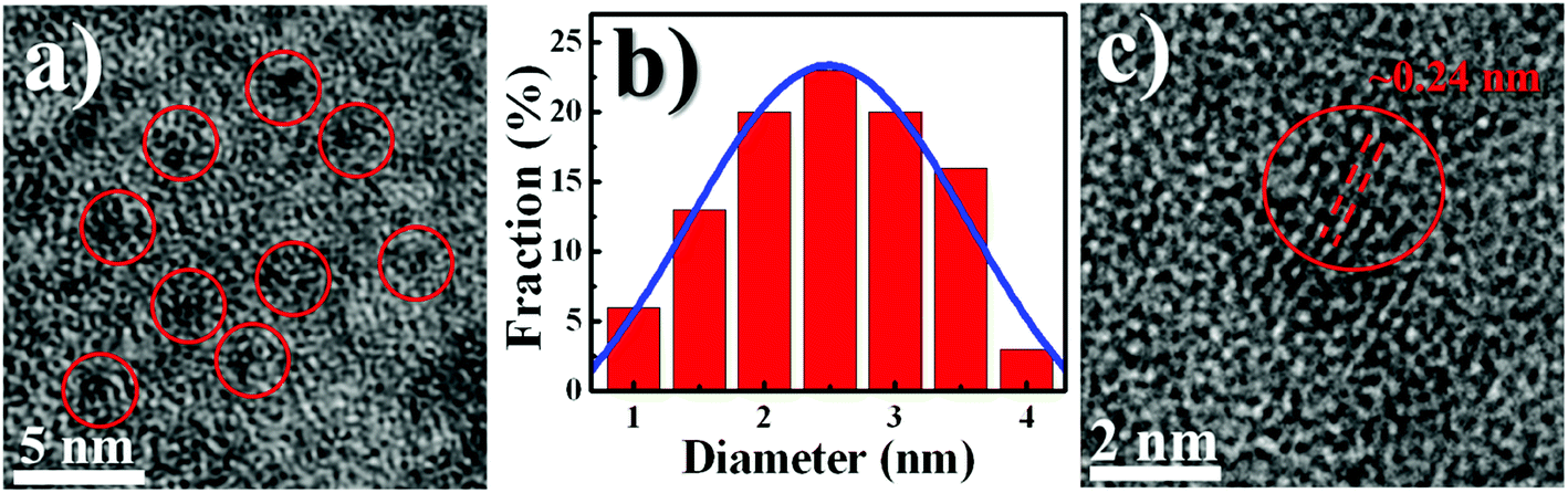
Fig. 1a shows the TEM image of WS2 QDs, demonstrating that WS2 QDs are dispersed with a size distribution ranging from 1 to 4 nm. An average diameter of WS2 QDs was found to be 2.5 ± 0.4 nm according to the Gaussian fit as depicted in Fig. 1b. This average size is comparable with the result of Ghorai et al., where the size of their WS2 QDs produced by prolonged sonication is around 3.5 nm.15 The high resolution TEM (HRTEM) image of WS2 QDs, shown in Fig. 1c, displays a lattice spacing of ∼0.24 nm, in agreement to the earlier work in Lin et al.17
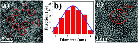 |
| | Fig. 1 (a) TEM image, (b) Gaussian distribution of average diameter, and (c) HRTEM images of WS2 QDs synthesized by pulsed laser ablation (PLA). | |
Fig. 2 displays the data of the absorption and PL spectra of synthesized WS2 QDs. The absorption spectrum demonstrates a peak at ∼230 nm and a shoulder at ∼290 nm. The cutoff of wavelength at 200 nm is due to instrument limit of detection in the spectrophotometer. The peak at ∼230 nm is attributed to the strong quantum confinement effect due to the small size of the WS2 QDs.18–20 While the shoulder peak at ∼275 nm is attributed to optical transitions between the density of states in the valence and conduction band.16 Previous studies have reported that WS2 QDs, synthesized through different methods, emit blue luminescence mostly. Likewise, WS2 QDs synthesized via PLA exhibit an emission peak at 360 nm under the excitation wavelength of 300 nm, as shown in Fig. 2.
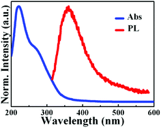 |
| | Fig. 2 Absorbance and photoluminescence (PL) spectra of WS2 QDs. | |
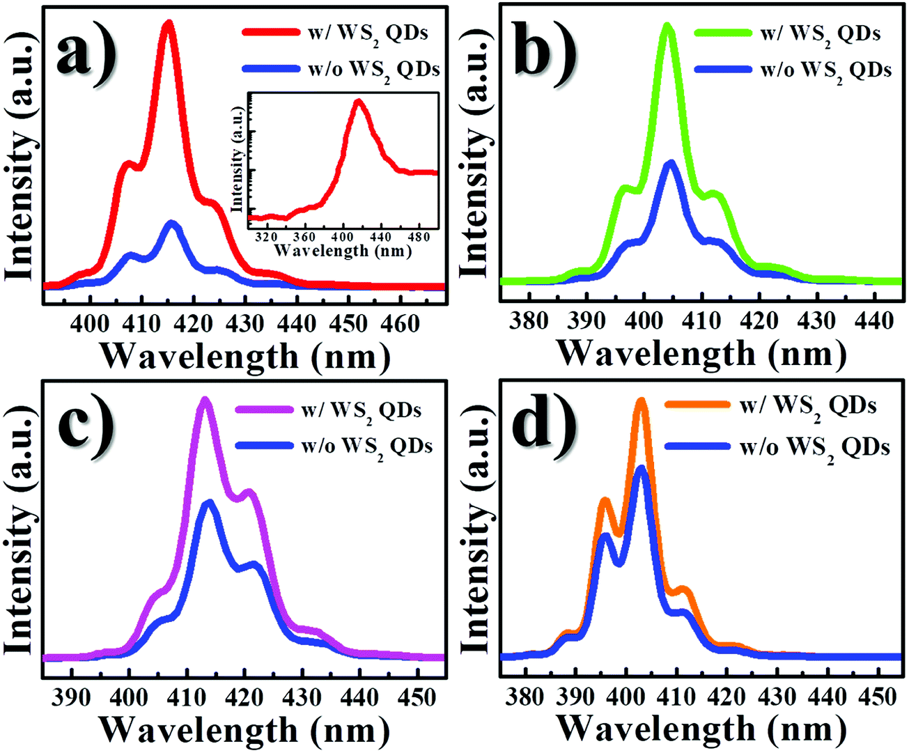
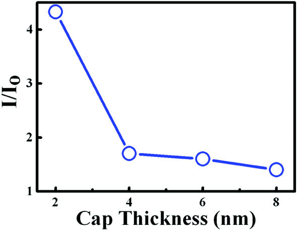
Fig. 3 displays the PL spectra of the bare InGaN QW and the InGaN QW with WS2 QDs, where the thickness of dsp ranges from 2 to 8 nm. After introduction of WS2 QDs, an increase of the PL intensity in the InGaN QW was observed. Fig. 4 shows the PL intensity ratio of the InGaN QW with WS2 QDs to that of without WS2 QDs as a function of dsp. The enhancement of PL intensity reveals a 4.3, 1.7, 1.6, and 1.4 fold for the InGaN-QW sample with dsp = 2, 4, 6, and 8 nm, respectively. The cap thickness (dsp) thus plays an important role for controlling the charge carriers in the InGaN QW since the PL intensity is associated with the charge carrier density. It is noted that the PL from WS2 QDs is unnoticeable for the InGaN QW with WS2 QDs, as shown in the inset of the Fig. 3(a). The PL in WS2 QDs is supposed to appear at 360 nm (from Fig. 2), but no obvious PL signal was observed at that wavelength. The PL emitted from WS2 QDs could be merged by the strong PL of the InGaN QW, which has high luminescence efficiency.
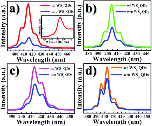 |
| | Fig. 3 PL spectra of bare InGaN/GaN QWs (blue line) and InGaN/GaN QWs with WS2 QDs. The cap layer thickness (barrier) of InGaN/GaN QW is (a) 2 nm; (b) 4 nm; (c) 6 nm; and (d) 8 nm, respectively. The inset in (a) shows the semilog plot of the PL spectrum in InGaN/GaN QWs with WS2 QDs ranging from 300 to 500 nm. | |
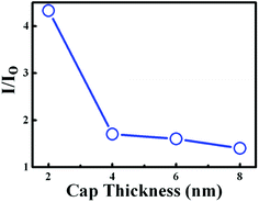 |
| | Fig. 4 PL intensity ratio of InGaN/GaN QWs with WS2 QDs to that of bare InGaN/GaN QWs as a function of cap thickness. The line is a guide for the eye. | |
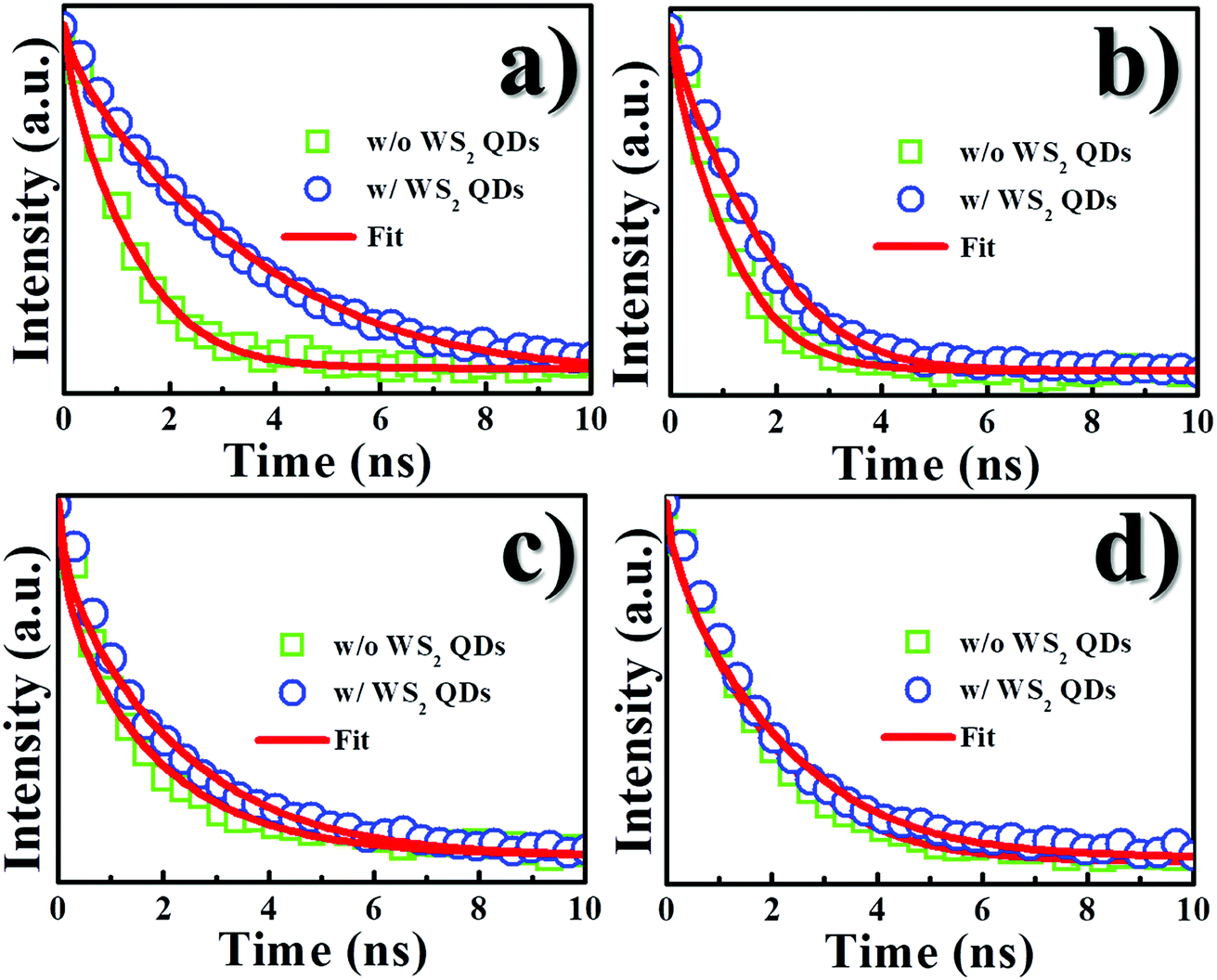
To further explore the carrier dynamics in InGaN QWs, time-resolved PL measurements were performed. Fig. 5(a)–(d) represents the PL transient of the InGaN QW with WS2 QDs having a spacer thickness of 2, 4, 6, and 8 nm, respectively, under a detection wavelength at the PL peak. The open squares represent bare InGaN QW while the open circles represent InGaN QW with the injection of WS2 QDs. It was found the PL transients of the InGaN QWs with WS2 QDs decay less as compared with that in bare InGaN QWs. The red lines in Fig. 5 represent the fits of PL decay curves using a stretch exponential function:21
| | |
n(t) = n(0)exp[−(kt)β]
| (1) |
where
n,
k and
β represent the carrier densities, the decay rate and the dispersive component, respectively. In a stretched exponential function, the average decay time
τPL can be obtained by:
22| |
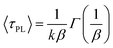 | (2) |
where
Γ is the Gamma function. The calculated
β,
k, and 〈
τPL〉 from the PL decays in
Fig. 5 are shown in
Table 1. It was found the difference of average decay time between the InGaN QW associated with WS
2 QDs and the bare InGaN QW is pronounced with decreasing
dsp. This gives an evidence that the increased carriers are injected into the InGaN QWs from WS
2 QDs, leading to an increase of the PL decay time. The amount of injected carriers enhances more pronouncedly as the barrier thickness decreases. Thus, the decay of PL reflects the competition between two processes: the recombination in the QW and the carrier transfer from WS
2 QDs.
 |
| | Fig. 5 PL transients of bare InGaN/GaN QWs (green squares) and InGaN/GaN QWs with WS2 QDs (blue circles) with the cap thickness of (a) 2 nm; (b) 4 nm; (c) 6 nm; and (d) 8 nm. Red lines represent fits of simulated data using eqn (1). | |
Table 1 The calculated dispersion component (β), decay rates (k), and average decay time (τPL)
| Barrier thickness (nm) |
Without WS2 QDs |
With WS2 QDs |
| β |
K (ns−1) |
τPL (ns) |
β |
K (ns−1) |
τPL (ns) |
| 2 |
0.65 |
4.545 |
0.301 |
0.67 |
1.667 |
0.793 |
| 4 |
0.67 |
4.76 |
0.278 |
0.64 |
2.123 |
0.471 |
| 6 |
0.48 |
7.69 |
0.281 |
0.535 |
4.347 |
0.401 |
| 8 |
0.68 |
5.26 |
0.247 |
0.59 |
5.26 |
0.292 |
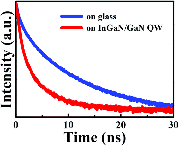
To find out whether the increased carriers in the InGaN QW stemmed from WS2 QDs, the PL dynamics of WS2 QDs was investigated. Fig. 6 shows the PL decay transients of WS2 QDs deposited on a glass and on the InGaN/GaN QW (barrier thickness = 2 nm) under the detection at the emission wavelength of 420 nm. The PL decay time of WS2 QDs on the InGaN/GaN QW was found to decrease drastically compared to that on the glass. This indicates the carriers in WS2 QDs on the InGaN/GaN QW have escaped out of QDs efficiently, producing a reduction of PL decay time. The decrease of the PL decay time in WS2 QDs concurrent to the increase of PL decay time in InGaN/GaN QW reveals that carrier transfer may take place from WS2 QDs to InGaN/GaN QW.
 |
| | Fig. 6 PL transients of WS2 QDs on a glass substrate and on the InGaN/GaN QW sample (cap thickness = 2 nm). | |
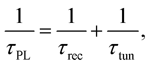
From the above data (Fig. 3, 5 and 6) we suggest that the enhanced PL intensity and PL decay time in the InGaN QW are attributed to the transfer of the photogenerated carriers from WS2 QDs via tunnel injection. Thus, the carrier tunneling time τtun can be estimated by considering the total decay rate, τPL−1, is the sum of recombination decay rate, τrec−1, and the rate of carrier tunneling, τtun−1, using the following equation:
| |
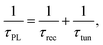 | (3) |
where
τPL is the measured PL decay time and
τrec is the recombination time. From
τPL of InGaN QWs without and with WS
2 QDs as well as
eqn (3),
τtun was determined and displayed in
Table 2.
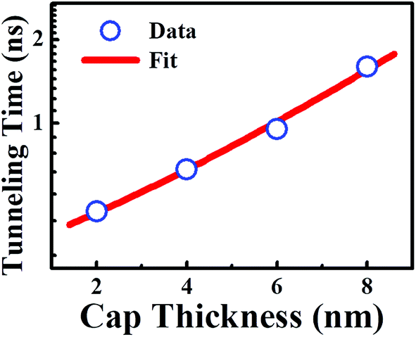
Fig. 7 displays the tunneling time as a function of barrier width, revealing an increase in the barrier thickness leads to an increase in the tunneling time.
Table 2 The calculated decay rates of InGaN/GaN QW, hybrids and tunneling time vs. cap (barrier) thickness
| Barrier thickness |
τPL |
τrec |
τtun |
| 2 |
0.301 |
0.793 |
0.48 |
| 4 |
0.278 |
0.471 |
0.69 |
| 6 |
0.281 |
0.409 |
0.95 |
| 8 |
0.247 |
0.292 |
1.6 |
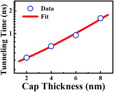 |
| | Fig. 7 Tunneling time calculated from the PL transient as a function of the cap thickness. Blue circles represent calculated data and red line represents the result of fits with WKB approximation (eqn (4)). | |
The dependence of the tunneling time on the barrier thickness may be comprehended with a semiclassical WKB model. In the WKB approximation, the tunneling time increases exponentially with the barrier thickness using the following relation:23,24
| |
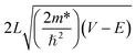 | (4) |
where
L is the barrier thickness,
m* is the effective mass in the barrier layer,
V is the band discontinuity of the conduction band (well depth), and
E is the lowest confinement energy level in the QW. This equation predicts a nearly linear relationship between
τT and
L. The dependence of the tunneling time
τtun on the barrier thickness was analyzed using the WKB approximation and shown as the solid line in
Fig. 7. A good fit to the experimental dependence of
τT on the
L is found. This confirms that mechanism of the carrier transfer from WS
2 QDs into InGaN QWs is governed by the tunneling. An increase in the barrier thickness leads to an increase of tunneling time, implying the tunneling coupling decreases as the barrier width increases. Similar results have been reported previously with regard to the carrier transfer
via tunneling.
24–26
To find out processes of the tunnel injection from WS2 QDs to InGaN/GaN QWs, the band diagram of InGaN/GaN QW was analyzed using APSYS simulation program,27 while the work functions of WS2 QDs as well as the GaN layer were measured using Kelvin probe. For the work function measurement, the contact potential difference (VCPD) between the sample and tip which is related to the difference in work function between the two is described by:26
| | |
eVCPD = Wtip − Wsample,
| (5) |
where
Wtip and
Wsample represents work functions of the tip and sample, respectively. The
Wsample can then be determined by calibration of
Wtip and
VCPD measurements. Using
eqn (5), the work function of WS
2 QDs was determined to be 4.77 ± 0.02 eV. While the work function of the GaN that serves as the barrier between WS
2 QDs and InGaN QWs is 4.38 ± 0.03 eV. Based on the work function results, we propose an energy diagram for the tunnel injection mechanism from WS
2 QDs to the InGaN QW, as displayed in
Fig. 8. Under photoexcitation with the photon energy greater than that of the bandgap in WS
2 QDs, electrons from QDs are generated. The WS
2 QDs can act as energy injectors, transferring their photogenerated electrons into the InGaN QW
via a tunneling process (the dashed arrow). Concurrently, the photogenerated holes in WS
2 QDs can move into the InGaN QW since the valence band in InGaN QW has a lower energy state compared to that in WS
2 QDs. When the transferred electrons and holes recombine in the InGaN QW, the PL intensity and PL decay time of the InGaN QW (the light emitter) are enhanced accordingly. The efficient tunneling injection from WS
2 QDs to InGaN QWs demonstrates that the tunnel-injection nanostructures including WS
2 QDs and InGaN QWs could be a candidate for realizing high-efficiency light emitting devices.
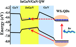 |
| | Fig. 8 Proposed diagram of carrier transfer via tunneling from WS2 QDs to InGaN/GaN QWs. | |
4. Conclusion
We have investigated a tunnel-injection structure including the injector of WS2 QDs, the barrier of GaN layers, and the light emitter of InGaN QWs. Steady state and time-resolved PL were used to characterize the tunnel injection process. A simultaneous increase in the PL intensity and PL decay time in InGaN QWs were observed in the presence of WS2 QDs. The tunneling time as a function of the barrier thickness has been determined, which agrees well with the WKB approximation. This study reveals that the tunnel-injection structure containing WS2 QDs and InGaN QWs is promising for their potential applications in the design of active layer in light emitting devices.
Conflicts of interest
There are no conflicts of interest to declare.
Acknowledgements
This project was supported in part by the Ministry of Science and Technology (Taiwan) under the grant number MOST 106-2112-M-033-009-MY3.
References
- X. Li, M. Rui, J. Song, Z. Shen and H. Zeng, Adv. Funct. Mater., 2015, 25, 4929–4947 CrossRef CAS
 .
. - S. Bley, M. Diez, F. Albrecht, S. Resch, S. R. Waldvogel, A. Menzel, M. Zacharias, J. Gutowski and T. Voss, J. Phys. Chem. C, 2015, 119, 15627–15635 CAS .
- J. S. Lee, M. V. Kovalenko, J. Huang, D. S. Chung and D. V. Talapin, Nat. Nanotechnol., 2011, 9, 348–352 CrossRef PubMed .
- W. Jieab and J. Hao, Nanoscale, 2014, 6, 6346–6362 RSC .
- I. Nikitskiy, S. Goossens, D. Kufer, T. Lasanta, G. Navickaite, F. H. L. Koppens and G. Konstantatos, Nat. Commun., 2016, 7, 11954 CrossRef CAS PubMed .
- S. Kang, A. Mandal, J. H. Chu, J. H. Park, S. Y. Kwon and C. R. Lee, Sci. Rep., 2015, 5, 10808 CrossRef CAS PubMed .
- Y. Lin, X. Li, D. Xie, T. Feng, Y. Chen, R. Song, H. Tian, T. Ren, M. Zhong, K. Wang and H. Zhu, Energy Environ. Sci., 2013, 6, 108–115 CAS .
- Z. Yin, H. Li, H. Li, H. Jiang, Y. Shi, Y. Sun, G. Lu, Q. Zhang, X. Chen and H. Zhang, ACS Nano, 2012, 6, 74–80 CrossRef CAS PubMed .
- S. Xu, D. Li and P. Wu, Adv. Funct. Mater., 2015, 25, 1127–1136 CrossRef .
- W. Gu, Y. Yan, C. Zhang, C. Ding and Y. Xian, ACS Appl. Mater. Interfaces, 2016, 8, 11272–11279 CAS .
- X. Wang, G. Sun, N. Lia and P. Chen, Chem. Soc. Rev., 2016, 45, 2239–2262 RSC .
- X. Bai, J. Wang, X. Mu, J. Yang, H. Liu, F. Xu, Y. Jing, L. Liu, X. Xue, H. Dai, Q. Liu, Y. M. Sun, C. Liu and X. D. Zhang, ACS Biomater. Sci. Eng., 2017, 3, 460–470 CrossRef CAS .
- X. Zhang, Z. Lai, Z. Liu, C. Tan, Y. Huang, B. Li, M. Zhao, L. Xie, W. Huang and H. Zhang, Angew. Chem., Int. Ed., 2015, 54, 5425–5428 CrossRef CAS PubMed .
- A. Ramasubramaniam, Phys. Rev. B: Condens. Matter Mater. Phys., 2012, 86, 115409 CrossRef .
- A. Ghorai, S. Bayan, N. Gogurla, A. Midya and S. K. Ray, ACS Appl. Mater. Interfaces, 2017, 9, 558–565 CAS .
- A. M. Rivera, A. P. S. Gaur, S. Sahoo and R. S. Katiyar, J. Appl. Phys., 2016, 120, 105102 CrossRef .
- L. Lin, Y. Xu, S. Zhang, I. M. Ross, A. C. M. Ong and D. A. Allwood, ACS Nano, 2013, 7, 8214–8223 CrossRef CAS PubMed .
- A. Bayat and E. Saievar-Iranizad, J. Lumin., 2017, 185, 236–240 CrossRef CAS .
- M. J. Kim, S. J. Jeon, T. W. Kang, J. M. Ju, D. Yim, H. I. Kim, J. H. Park and J. H. Kim, ACS Appl. Mater. Interfaces, 2017, 9, 12316–12323 CAS .
- J. P. Wilcoxon and G. A. Samara, Phys. Rev. B: Condens. Matter Mater. Phys., 1995, 51, 7299 CrossRef CAS .
- Y. N. Hao, H. L. Guo, L. Tian and X. Kang, RSC Adv., 2015, 5, 43750–43755 RSC .
- A. F. van Driel, I. S. Nikolaev, P. Vergeer, P. Lodahl, D. Vanmaekelbergh and W. L. Vos, Phys. Rev. B: Condens. Matter Mater. Phys., 2007, 75, 035329 CrossRef .
- Y. L. Mazur, Z. M. Wang, G. G. Tarasov, G. J. Salamo, J. W. Tomm and V. Talalaev, Phys. Rev. B: Condens. Matter Mater. Phys., 2005, 71, 235313 CrossRef .
- R. Naouari, W. Ouerghui, J. Martinez-Pastor, J. G. Brescó, M. A. Mareef, D. Gradanos and J. M. Garcia-Martinez, J. Mod. Phys., 2012, 3, 471–475 CrossRef CAS .
- V. G. Talalaev, J. W. Tomm, N. D. Zakharov, P. Werner, U. Gösele, B. V. Novikov, A. S. Sokolov, Y. B. Samsonenko, V. A. Egorov and G. E. Cirlin, Appl. Phys. Lett., 2008, 93, 031105 CrossRef .
- T. N. Lin, M. R. Inciong, S. R. M. S. Santiago, T. W. Yeh, W. Y. Yang, C. T. Yuan, J. L. Shen, H. C. Kuo and C. H. Chiu, Sci. Rep., 2016, 6, 23260 CrossRef CAS PubMed .
- C. H. Wang, C. C. Ke, Y. Lee, S. P. Chang, W. T. Chang, J. C. Li, Z. Y. Li, H. C. Yang, H. C. Kuo, T. C. Lu and S. C. Wang, Appl. Phys. Lett., 2010, 97, 261103 CrossRef .
|
| This journal is © The Royal Society of Chemistry 2018 |
Click here to see how this site uses Cookies. View our privacy policy here. 
 Open Access Article
 This Open Access Article is licensed under a
  *a,
Ching-Hsueh Chiub and
Hao-Chung Kuoc
*a,
Ching-Hsueh Chiub and
Hao-Chung Kuoc