
 Open Access Article
 This Open Access Article is licensed under a
 Creative Commons Attribution 3.0 Unported Licence
Formation of intrinsic and silicon defects in MoO3 under varied oxygen partial pressure and temperature conditions: an ab initio DFT investigation
D. S. Lambert *a,
S. T. Murphyb,
A. Lennona and
P. A. Burrc
*a,
S. T. Murphyb,
A. Lennona and
P. A. Burrc
aSchool of Photovoltaics and Renewable Energy Engineering, The University of New South Wales, Sydney, NSW 2052, Australia. E-mail: d.lambert@student.unsw.edu.au
bDepartment of Engineering, Lancaster University, Bailrigg, Lancaster, LA1 4YW, UK
cSchool of Electrical Engineering and Telecommunications, The University of New South Wales, Sydney, NSW 2052, Australia
First published on 23rd November 2017
Abstract
Molybdenum trioxide (MoO3) is a promising material for energy conversion applications, including recent uses as a hole selective contact in silicon photovoltaic devices. The electrical and chemical properties of MoO3 are known to be strongly sensitive to the presence of intrinsic and extrinsic defects, which in turn are dependent on the fabrication route and processing conditions used to form the device layers. Of particular interest to this study were intrinsic defects comprising oxygen vacancies and extrinsic defects involving possible contaminant silicon atoms. Density functional theory simulations were used to predict defect concentrations as a function of processing temperature and oxygen partial pressure. A rigorous method is outlined to calculate defect formation energies for all intrinsic defects in MoO3, resolving conflicting information arising from previous studies. Brouwer diagrams were constructed and used to show that the charge neutral oxygen vacancy is dominant under most of the temperature and oxygen partial pressure conditions investigated. It was also shown that at commonly-used processing temperatures and oxygen partial pressures, silicon interstitials in MoO3 can introduce a spin-polarised defect state 0.5 eV above the MoO3 valence band maximum. Their concentration in MoO3 may reach 1.3 ppm with processing conditions of 700 K and 10−6 atm oxygen partial pressure, and this concentration is predicted to increase dramatically with higher temperatures and/or lower oxygen partial pressures. Our findings highlight the possibility of silicon contamination in hole-selective contact layers for silicon photovoltaic devices, with a potential increase in the parasitic absorption due to silicon defects in the contact layers reducing energy conversion efficiency.
Introduction
The worldwide search for efficient and cost-effective energy conversion and storage systems has resulted in the investigation of new uses for lesser known materials. Molybdenum trioxide and its sub-stoichiometric form (MoO3−x; 0 < x < 1) is a material with proposed applications in batteries,1–3 electrochemical capacitors,4–8 sensors,9,10 catalysis,11–13 photo-catalysis,14,15 electrochromism and photochromism.16–18 It has also been found to be an effective hole transport layer in semiconductor devices19–21 and a range of photovoltaic cells.20–22Sub-stoichiometric molybdenum trioxide was first reported as a contact layer for organic,23–25 kesterite26 and perovskite27–30 solar cells, however recently it has also found application as a hole-selective contact for higher efficiency silicon heterojunction cells. It has a large workfunction of 5.7 eV and wide band gap of 3.3 eV, which allows an electrical contact to achieve high hole selectivity without inducing significant parasitic absorption.22 Battaglia et al.22 found that by replacing the p-type amorphous silicon hole contact layer with amorphous MoO3−x, the short circuit current density could be increased by 1.9 mA cm−2, although a reduction in fill factor degraded the overall efficiency. The low fill factor was subsequently addressed by Geissbühler et al.31 by limiting the processing temperature for devices to 130 °C. This enabled them to achieve an energy conversion efficiency of 22.5% for silicon heterojunction cells. However, this achievement still falls short of the record efficiency of 24.7%![[thin space (1/6-em)]](https://www.rsc.org/images/entities/char_2009.gif) 32 for a two-side contacted heterojunction cell, and the low processing temperature is incompatible with other manufacturing processes such as silver screen-printing. In order to overcome these problems, Cauduro et al.33 recently proposed that controllable crystallisation of reactive-sputtered films of MoO3−x can be used to form films with a high workfunction and a highly ordered nanocrystalline sublayer structure that may enhance carrier mobility and allow for higher processing temperatures. Sook et al.34 have also reported that crystalline MoO3−x has improved mobility and lower resistivity than amorphous MoO3−x, and has material properties that are highly dependent on preparation conditions. Consequently, in order to realise the full potential of MoO3−x as a low-cost hole transport layer for silicon solar cells, it is necessary to understand how preparation conditions affect the material's structural and electrical properties, as well as it’s compatibility with silicon substrates.
32 for a two-side contacted heterojunction cell, and the low processing temperature is incompatible with other manufacturing processes such as silver screen-printing. In order to overcome these problems, Cauduro et al.33 recently proposed that controllable crystallisation of reactive-sputtered films of MoO3−x can be used to form films with a high workfunction and a highly ordered nanocrystalline sublayer structure that may enhance carrier mobility and allow for higher processing temperatures. Sook et al.34 have also reported that crystalline MoO3−x has improved mobility and lower resistivity than amorphous MoO3−x, and has material properties that are highly dependent on preparation conditions. Consequently, in order to realise the full potential of MoO3−x as a low-cost hole transport layer for silicon solar cells, it is necessary to understand how preparation conditions affect the material's structural and electrical properties, as well as it’s compatibility with silicon substrates.
Sub-stoichiometric molybdenum trioxide can be prepared by a number of techniques such as thermal oxidation,35 spray pyrolysis,36 or reactive sputtering.34,37 The most common preparation method involves a two-step process, where MoO3 powder is first thermally-evaporated onto a substrate, and then the resulting film is annealed at high temperature.38,39 The conditions of preparation affects the defect chemistry, in particular by the formation of oxygen vacancies35 and, if enough vacancies form, then the material can amorphize.40 The stoichiometry of MoO3−x has been shown to influence many important properties of the material, such as work function,35 battery capacity,41 band gap,38,42,43 conductivity,44 and optical reflectance.45 Point defects are also believed to create a defect band within the band gap of MoO3−x, which is thought to be crucial for selective carrier extraction.22 A mechanistic understanding of the sensitivity of defect chemistry to deposition method and post-deposition processing is needed in order to tailor the properties of MoO3−x for device applications.
Crystalline α-MoO3 has a structure consisting of layers of distorted octahedral, joined along the b-axis by van der Waals forces, as shown in Fig. 1. Three distinct oxygen sites exist in MoO3, with different coordination. The O1 oxygen atom, sometimes referred to as the terminal oxygen, is connected to only one Mo atom and extends along the b-axis into the van der Waals planes. The O2 oxygen atom, also known as the asymmetric oxygen, has two bonds to molybdenum atoms, of different length. The O3 atom is triply coordinated and has been called the symmetric oxygen, as the in-plane bonds with molybdenum atoms are the same length. Oxygen vacancies may form at each of these sites.
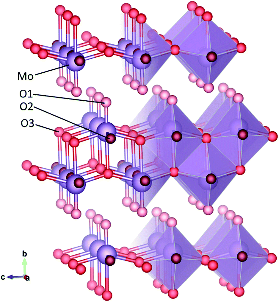 | ||
| Fig. 1 Structure of crystalline MoO3 in ball-and-stick and polyhedral representation. The molybdenum (Mo) atom is in purple and the three oxygen (O) sites are in three different shades of red. | ||
Density functional theory (DFT) calculations have been used to determine the oxygen vacancy formation energies at each site in previous studies,46–49 however these studies have used different methodologies and yielded results that are highly inconsistent with each other. The formation energy of molybdenum vacancies was considered in one study,48 but the formation energy of molybdenum and oxygen interstitials is still not known. In this study, a well-defined and consistent method is used to analyse the formation energy of all intrinsic defects, and then these are related to real-life defect concentrations at various experimental conditions of temperature and oxygen partial pressure through the construction of Brouwer diagrams.
Since many of the selective contact applications involve MoO3−x in contact with silicon surfaces,20,22 silicon defects within bulk MoO3 are also studied in this paper. A study by Anwar et al.50 on Si–MoO3 mixtures suggested that silicon atoms may penetrate MoO3 and that these atoms could reduce the electrical conductivity. Previously, extrinsic defects in MoO3 crystals such as Na,47 Li3,51 and H52,53 have been studied with DFT, but so far DFT studies of the interaction between MoO3 and silicon have only examined molybdenum oxides on silica surfaces.54–56 In this paper, the possibility of silicon diffusion in crystalline MoO3 is investigated and its effect on electronic properties is explored.
Methodology
Computational details
Density functional theory calculations were performed with the projector augmented wave approach using the Vienna ab-initio simulation package (VASP).57 Simulations in DFT require the choice of an exchange–correlation functional among other important parameters in order to balance accuracy with computational complexity. For this study, the PBE-GGA functional58 was used with the addition of an on-site Coulomb correction (+U) of 6.3 eV in order to improve the localisation of d-electrons in molybdenum using the simplified rotationally invariant formalism of Dudarev et al.59 in line with previous work on MoO3.52,60,61 In order to account for the significant effect of van der Waals forces in this material, the semi-empirical DFT-D3 energy correction by Grimme et al.62 was used. While a number of different parameters have been used in the modelling of MoO3 in the past, as is outlined in the Model verification subsection, the parameters chosen for this paper provide accurate results without excessively long simulation times.The Brillouin zone was sampled with a 3 × 1 × 2 k-point mesh for the supercell of choice, 2 × 2 × 3. The choice of supercell shape and size is justified in the subsection Charge correction. Simulations were performed with a plane wave basis set energy cut-off of 500 eV, and a Gaussian smearing of the partial occupancies was applied with a width of 0.1 eV to speed up the simulations. The density of states were obtained by performing an additional single point calculation after geometry optimisation using a denser k-point mesh of 6 × 2 × 4 k-points and interpolating with the tetrahedron method with Blöchl corrections. The static ion-clamped dielectric tensor and elastic constants were calculated with density functional perturbation theory. For elastic constant calculations, both lattice and atoms were displaced in steps of ±0.005 Å and ±0.01 Å.
Formation energies
Defect formation energies were calculated according to eqn (1)
 | (1) |
Chemical potentials
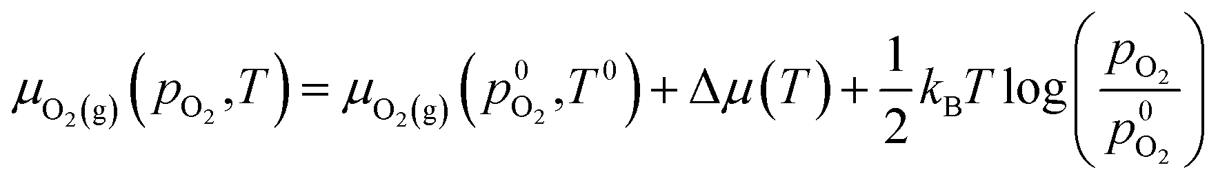
The chemical potentials used in eqn (1) have a large effect on defect formation energies, and must be determined carefully. The chemical potentials of molybdenum and oxygen atoms within the MoO3 crystal are derived from the chemical potentials of the same atoms in reservoirs of BCC-Mo(s) crystal and O2(g) respectively. To overcome the well-known limitation of GGA-DFT inaccurately modelling oxygen gas molecules,63 the method of Finnis et al.64 is used to derive the chemical potential of oxygen in O2 gas, μO2(g), from the equation for standard formation energy of MoO3:
 | (2) |
 is the experimental standard formation energy of MoO3 with a value of −668.079 kJ mol−1,65 and the chemical potentials μMoO3(s) and μMo(s) are the DFT total energies of MoO3 and BCC-Mo respectively, normalised per formula unit. The assumption is made that the chemical potentials of the MoO3 and BCC-Mo(s) crystals are not strongly dependent on partial pressure and temperature, but that the potential of the oxygen gas will change according to the rigid-dumbbell ideal gas law:
 | (3) |
 | (4) |
To test these assumptions, the expected free energy of formation at 700 K was calculated with eqn (2)–(4) to be −588 kJ mol−1, close to the experimental value of −567 kJ mol−1.65
The total chemical potential of a formula unit of MoO3 is the sum of the chemical potentials of its component parts inside the MoO3 crystal:
| μMoO3(s) = μMo(MoO3) + 3μO(MoO3) | (5) |
At equilibrium, the chemical potentials of atoms inside the crystal cannot be larger than that of the reservoirs outside. Within these bounding cases, the assumption is made that the chemical potential of oxygen in MoO3 is equal to that of oxygen gas, which better describes the case of O-rich condition. Thus, the chemical potentials of oxygen and molybdenum in MoO3 are:
| μO2(MoO3)(pO2,T) = μO2(g)(pO2,T) | (6) |
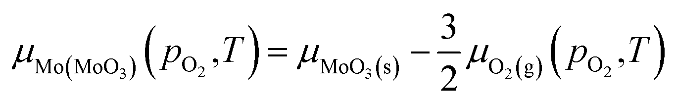 | (7) |
Where silicon impurities are considered, the chemical potential of silicon was calculated with the same procedure from DFT simulations of α-quartz SiO2, and assuming that it was in equilibrium with oxygen gas.
Charge correction
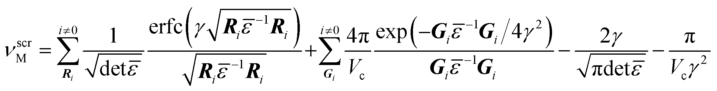
When charge is introduced into a supercell with periodic boundary conditions, an energy shift results from both the charge interaction between the repeating cells63 and from the background uniform charge jellium introduced to compensate for this.66 The magnitude of the required correction is a function of the screened Madelung potential, νscrM, calculated in an anisotropic medium with the following equation:67
 | (8) |
![[small epsilon, Greek, macron]](https://www.rsc.org/images/entities/i_char_e0c6.gif) is the dielectric tensor. Thus, in an anisotropic medium, the Madelung potential can be zero or negative for certain lattice vectors.66 To demonstrate the effect of Madelung potential, the +1 charged O1 oxygen vacancy (
is the dielectric tensor. Thus, in an anisotropic medium, the Madelung potential can be zero or negative for certain lattice vectors.66 To demonstrate the effect of Madelung potential, the +1 charged O1 oxygen vacancy ( using Kröger–Vink notation68) was simulated in different supercell sizes and shapes. The resulting formation energy is shown as a function of the Madelung potential in Fig. 2. The uncorrected formation energy when using a 3 × 1 × 3 supercell is 0.25 eV lower than that from a 2 × 2 × 3 supercell. The amount of correction required is proportional to the square of the amount of charge introduced,69 so for simulations involving high charges such as
  or
or  it is essential to have an accurate method of correcting for charged defects.
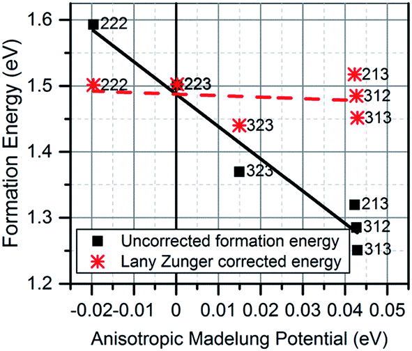 | ||
Fig. 2 Defect formation energy of  as a function of Madelung potential, before (black solid) and after (red dashed) applying the approximate Lany and Zunger charge correction.70 The labels indicate the dimensions of the supercell used (in terms of unit cell replicas). as a function of Madelung potential, before (black solid) and after (red dashed) applying the approximate Lany and Zunger charge correction.70 The labels indicate the dimensions of the supercell used (in terms of unit cell replicas). | ||
The 3 × 1 × 3 supercell has nearly equal simulation lengths in the a, b, and c directions, and has been used by most previous studies to model point defects.47,48 However, when considering the anisotropic character of the dielectric constant, it is apparent that the 2 × 2 × 3 supercell has near-zero Madelung potential, yielding a very small Coulomb self-interaction energy. For the very highly charged defect of  , a first order approximation to the charge correction yields a charge correction less than 0.5 eV, and it has been shown that this is an overcorrection that should be scaled down further to correct for local screening,70 indicating that the use of this supercell shape removes almost all of the uncertainties associated with the use of approximate charge correction schemes.
It is important to note that finite size effects may also arise from elastic self-interaction,71,72 which are dependent on the anisotropic elastic constant tensor. Since the elastic tensor is distinctly different from the dielectric tensor, a compromise must be struck between elastic and electrostatic self-interaction when choosing the optimal supercell shape. Nevertheless, the moderate permittivity and comparatively large stiffness of MoO3, shown in Tables 1 and 2, means that the magnitude of the charge self-interaction energy is considerably larger than that of elastic self-interaction. Therefore, the current work was carried out using the 2 × 2 × 3 supercell.
| Direction | ε∞11 | ε∞22 | ε∞33 | Average |
|---|---|---|---|---|
| This work | 5.8 | 4.2 | 6.1 | 5.4 |
| Previous DFT | 5.5 | 4.2 | 6.3 | 5.3 |
| Experimental | — | — | — | 5.7 |
| c11 | c22 | c33 | c12 | c13 | c23 | c44 | c55 | c66 | K | G | E |
|---|---|---|---|---|---|---|---|---|---|---|---|
| 263 | 96 | 340 | 41 | 72 | 51 | 98 | 64 | 57 | 98 | 74 | 176 (65) |
The VO2 defects, which were stable in the 3 × 1 × 3 supercell, were not stable in this supercell, collapsing onto the O1 site. Akande et al.48 report nearly identical formation energies for vacancies on the O2 and O1 sites, suggesting that this collapse was not a unique feature of our methodology. Nevertheless, the VO2 defect formation energy was calculated in a larger supercells (4 × 4 × 6, 3 × 1 × 3, 2 × 2 × 2, 3 × 2 × 2), and it was consistently found to either collapse into VO1 or be much less favourable than VO1 for all charge states and in all supercell sizes investigated, thus the omission of these defects does not have a significant effect on the predicted defect concentrations.
Brouwer diagram
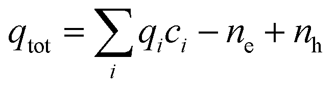
Brouwer diagrams provide a means for identifying the concentration of defects in a material to the environment's oxygen partial pressure and temperature. The defect formation energies calculated from the DFT simulation were used to construct Brouwer diagrams with the aid of a defect analysis package.76For each value of pO2 and T, there is only one Fermi level for which charge neutrality is conserved. Using an initial estimate for the Fermi level, the concentration of electrons and holes is calculated using the experimental bandgap according to Maxwell–Boltzmann statistics:
 | (9) |
 | (10) |
 | (11) |
 | (12) |
Results and discussion
Model verification
The calculated lattice parameters were 3.84 Å, 14.38 Å and 3.77 Å, for the a-axis, b-axis and c-axis respectively, which are all within 4% of the experimental values of 3.96 Å, 13.86 Å and 3.70 Å reported by Kihlborg et al.77 Fig. 3a and b compare the axis length and bond lengths calculated in the current work with previous computational reports as a percentage of the experimental values. The largest deviation for the axis lengths is observed in the b-axis, where the inter-planar distance is dominated by van der Waals interactions. To overcome this, previous studies have fixed the b-axis length to the experimental value47,61,78 resulting in larger bandgaps and lattice parameters which are in closer agreement with experimental values. However, a constrained structure necessarily has internal strains; in turn, these are known to affect the formation energy of the defects considerably, as noted by Huang et al.79 Therefore, all constraints were removed in this study when simulating the defect-free lattice.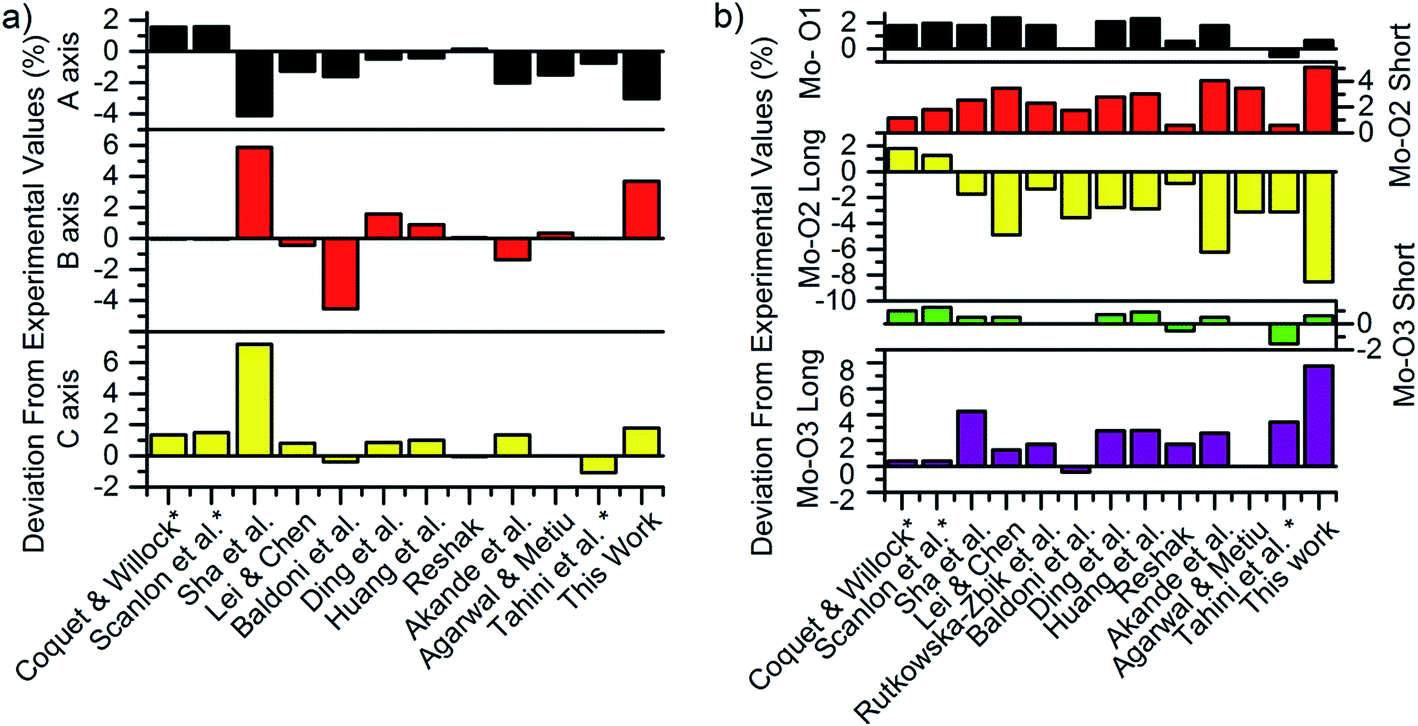 | ||
| Fig. 3 Deviation of calculated (a) axis lengths and (b) bond lengths compared to experiment for 12 previous studies and this work.47,48,51–53,60,61,79,82,83,87,88 Star symbols indicate studies that have constrained the b-axis to experimental value. | ||
The other major differences in axis lengths and bond-lengths that are evident in Fig. 3a and b are caused by differing choices of exchange–correlation functional, on-site Coulomb correction (+U) value, and van der Waals forces treatment. This work used the D3 treatment by Grimme,62 while earlier studies used the D2,47,80 the optB88-vdW46,81,82 or in the case of early studies,53,60,61 no treatment at all. The most common level of theory was GGA + U with a U parameter of 6.3 eV, however there were studies that used smaller U values,83 no U parameter53 or the HSE06 hybrid functional.48
The band gap of the simulated structure of this work was found to be 1.5 eV, which is lower than the experimental values that range from 3 to 3.3 eV.22,36,38,84 The underestimation of the bandgap is a well-known issue with DFT simulations employing local and semilocal exchange correlation functionals, and the band gap predicted here is close to other values using the same functional, such as the 1.6 eV reported by Huang et al.79 and the 1.7 eV reported by Peelaers et al.85 for the PBE functional. Studies that fixed the b-axis reported higher bandgaps of between 1.95 eV61 and 2.4 eV,47 in line with results showing that lattice distortion has a significant effect on bandgap.79 It has been shown that adding a +U correction only widens the computed gap by around 0.1 eV or so,51,52 while the use of the HSE06 hybrid functional produces bandgaps consistent with experimental value,47,48,85 at the cost of greatly increasing computational complexity.
With Bader analysis,86 the Bader charges on the oxygen atoms were found to be −0.68e, −0.99e and −1.10e, for the O1, O2 and O3 atoms respectively, with a Bader charge on the Mo of 2.77e. These results match within 8% the recent works of Agarwal et al.83 and Akande et al.,48 but have an up to 22% magnitude difference from older studies with no van der Waals treatment such as Coquet & Willock,60 Sha et al.,53 and Lei & Chen,52 indicating that van der Waals treatment has a noticeable effect on charge distributions in this material.
Fig. 4 shows the wide discrepancies in oxygen vacancy formation energies in the literature, such as the 2.1 eV difference between the formation energy reported on the  by Akande et al.48 and that reported in Kim et al.46 These variations are a considerably larger than what is acceptable for meaningful analysis of defect concentration, as there is an exponential dependence of concentration on formation energy. For example, using simple Boltzmann statistics at 300 K, a 1 eV drop in defect formation energy would multiply the predicted defect concentration by a factor of over 1017.
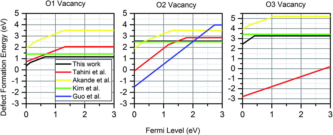 | ||
| Fig. 4 Comparison of oxygen vacancy formation energies for four previous studies46–49 and this work. Kim et al. only considered charge neutral vacancies. For the VO2, the stable charge neutral state shown is from a larger 4 × 4 × 6 supercell simulation. For studies with multiple charges, only the most dominant charge state at each Fermi level is shown. The values from this work are calculated at a temperature of 300 K and an oxygen partial pressure of 0.2 atm. | ||
These large defect formation differences are caused by variations of the parameters in eqn (1). The differences in the formation energy of charge neutral vacancies can only be explained by the differing methods of determining the oxygen chemical potential and the variations in computational method already discussed. The differences in the Fermi level at which the cross-over between two charge states occur, are not affected by the oxygen chemical potential, but may be explained by other factors. For example, the use of the 3 × 1 × 3 supercell size without charge correction would make the charged states appear more favourable than they are, as was shown in Fig. 2, making them dominant for larger Fermi levels than are found in this work. An underestimation of the electron potential at the valence band minimum would have the same effect.
Intrinsic defects
There are several types of intrinsic point defects that could occur in MoO3, consisting of vacancies and interstitials of molybdenum and oxygen atoms. There are three different types of VO2, corresponding to the three sites in α-MoO3 with different coordination numbers. Three stable sites for were found for Moi, shown in Fig. 5a, and three stable sites were found for Oi, shown in Fig. 5b. The Wyckoff positions for these interstitials are presented in Table 3.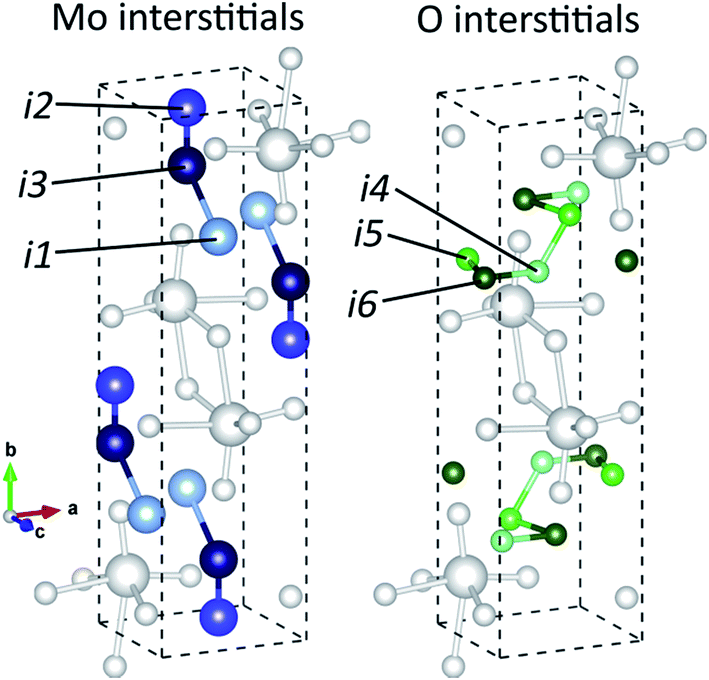 | ||
| Fig. 5 Interstitial sites found to be stable, with Mo/Si interstitial sites shown on the left in three shades of blue and O interstitial sites shown on the right in three shades of green. Mo and O atoms are shown in white. | ||
| Interstitial site | Location | Interstitial atoms stable at site |
|---|---|---|
| i1 | 4c (0.5, 0.25, 0.25) | Mo, Si |
| i2 | 4c (0.5, 0.0425, 0.25) | Mo, Si |
| i3 | 4c (0.5, 0.15, 0.75) | Mo, Si |
| i4 | 4c (0.625, 0.3, 0.25) | O |
| i5 | 4c (0.4, 0.2, 0.25) | O |
| i6 | 4c (0.5, 0.2, 0.75) | O |
Fig. 6 shows the defect formation energy at a temperature of 300 K and pO2 of 0.2 atm for the most favourable charge state of each intrinsic defect as a function of Fermi level. Oxygen vacancies are most easily accommodated on the O1 site, and may take all three charge states but the charge neutral state is predominant for the majority of electron energies in the bandgap. The i6 site was found to be the most favourable oxygen interstitial, although it is only slightly more favourable than Oi5. Oxygen interstitials are predicted to mostly exhibit the 0 and −2 charge state, with the Oi5 only exhibiting the charge neutral state. All oxygen interstitials exhibit highly unfavourable formation energies compared to the other defects. Molybdenum vacancies adopt all negative charge states except −4, and −6 while the dominant Moi3 adopts all positive charge states except +4 and +5.
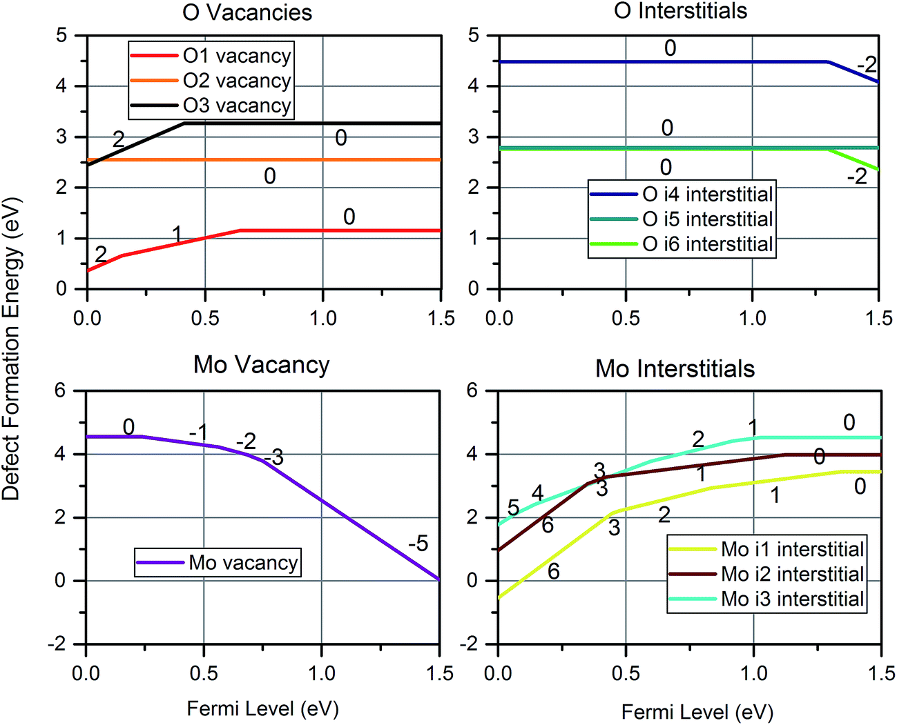 | ||
| Fig. 6 The formation energy of the dominantly charged defect at each Fermi level for each intrinsic defect at a temperature of 300 K and pO2 of 0.2 atm. The charges of the dominant charge states are labelled. | ||
The only other study that considered VMo was by Akande et al.,48 who predict formation energies in excess of 10 eV higher than the current work. Such large difference cannot be accounted for with the differences in DFT methodology, instead it is likely due to different treatment of the chemical potential. Comparison of formation energy differences between O-rich and O-poor conditions provides further insight: in our methodology, an increase of ΔE in μO(MoO3) yields a necessary decrease of 3ΔE in μMo(MoO3), as enforced through eqn (5). The same energy shift between O-rich and O-poor is not observed in the work of Akande et al., confirming the use of a different definition of chemical potential.
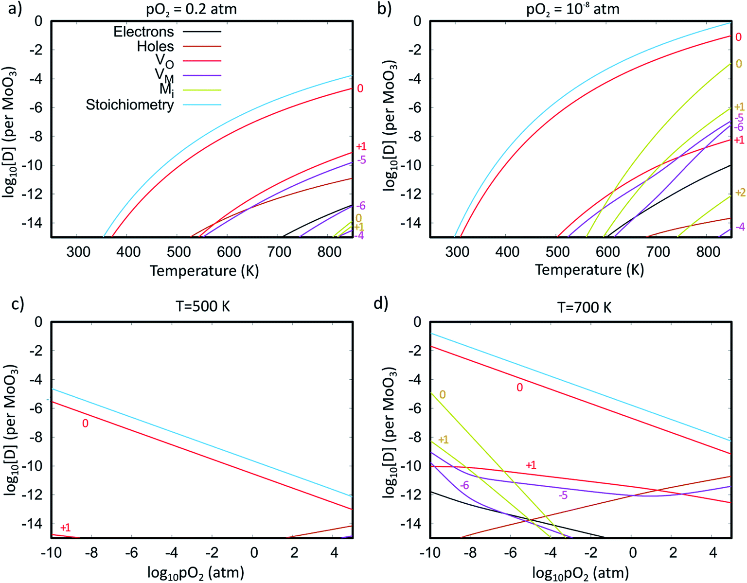
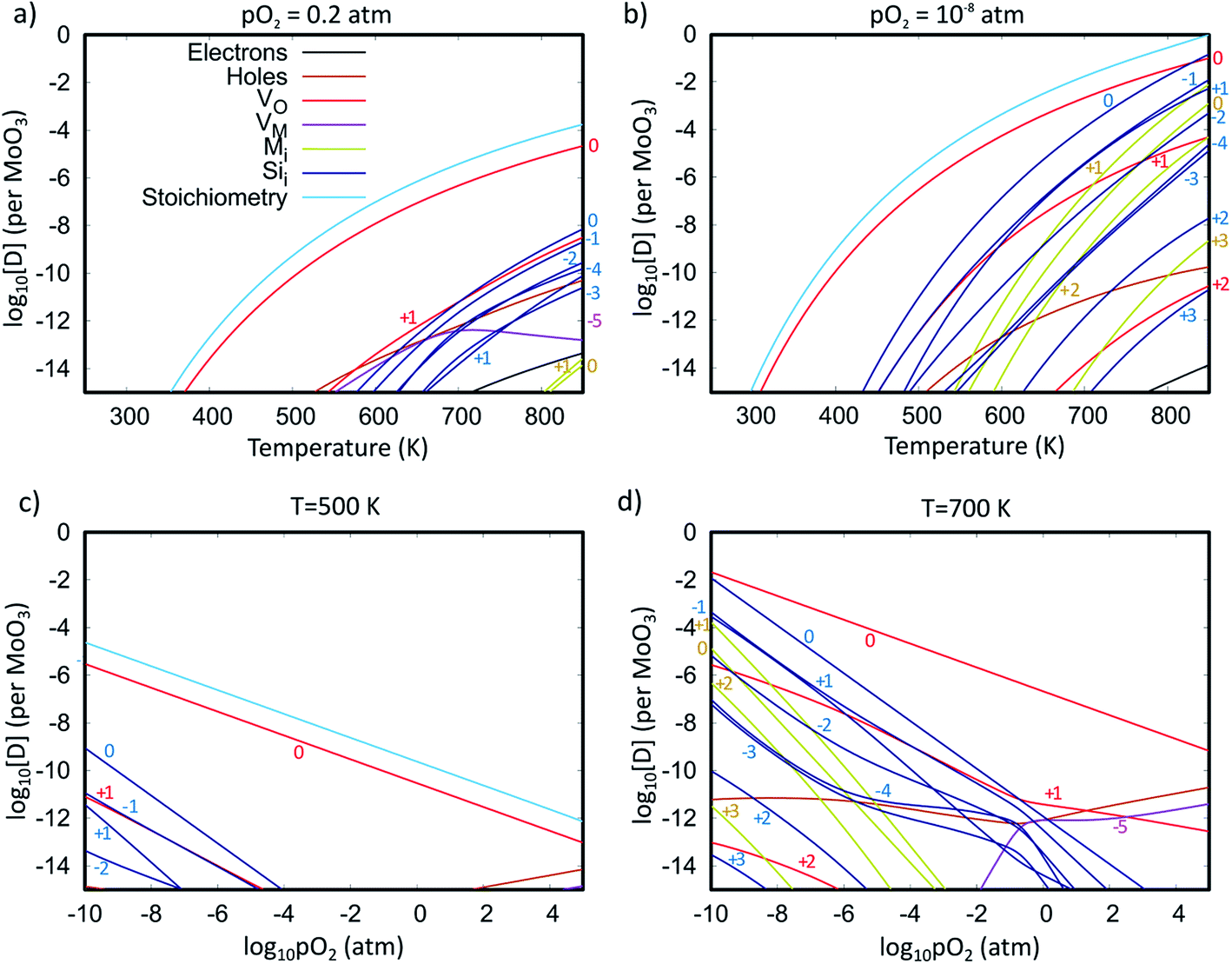
Fig. 7 shows the Brouwer diagrams of defect concentrations at different values of temperature and pO2. Fig. 7a shows that at atmospheric pressure, significant numbers of defects do not occur unless the temperature is elevated. The dominant defect by far is the charge neutral oxygen vacancy, with near-negligible amounts of  and
and  (two orders of magnitude less). These results match the experimental evidence that oxygen vacancies are the dominant defect in MoO3 films,89,90 and that the amount of oxygen vacancies is dependent on the pressure37 and temperature45 used in sample preparation. The current Brouwer diagrams provide a further clarification of this temperature and pressure dependence.
 | ||
| Fig. 7 Brouwer diagrams showing the defect concentrations per formula unit as a function of temperature at constant pressure of (a) 0.2 atm and (b) 10−8 atm, and as a function of partial pressure at constant temperatures of (c) 500 K and (d) 700 K. Graphs also include concentrations of electrons and holes and the degree of sub-stoichiometry (x in MoO3−x). The different charge states of each defect type are labelled. | ||
Fig. 7b shows that if a high temperature anneal is performed under low pressure or low oxygen conditions, a large number of  will form, along with some Moi. The number of oxygen vacancies predicted at the very highest temperatures in Fig. 7b, would make the crystalline structure completely unstable. This matches with the experimental observation that initial thermal evaporations at low pressures in the range of 10−9 atm always results in sub-stoichiometric amorphous materials.21,91,92 These results also are in agreement with the fact that annealing MoO3 at temperatures of above 550 K in argon atmosphere results in high levels of oxygen vacancies but similar anneals in oxygen atmospheres do not.36,40 It's worth noting that although the
  is dominant, the charged defects still play a crucial role in determining the Fermi energy that gives yields charge neutrality, which varies within the range of 1.1 eV to 1.9 eV for the pressures and temperatures considered.
Fig. 7c and d show how changing the oxygen partial pressure affects the concentration of defects significantly. The dominance of the  in the range examined gives us a simple formula for determining the effect of varying oxygen partial pressure: by combining eqn (1), (3) and (11), it can be determined that the concentration of vacancies is inversely proportional to the square root of oxygen partial pressure, eqn (13). This concentration will be the dominant factor affected the stoichiometry of the material.
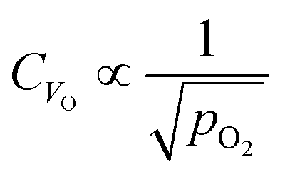 | (13) |
The accuracy of the estimated concentration of vacancies is hard to determine as there has been little quantification of defect concentrations in the experimental literature. Sian and Reddy91 found a degree of sub-stoichiometry x of 0.01 for material annealed in air at 623 K, four orders of magnitude higher than that predicted in Fig. 7. However, the discrepancy may be largely attributed to the reported incomplete crystallisation in the experiment. The Brouwer diagrams also indicate that trace levels of Moi defects may be observed at high temperature and low pO2, but no Oi defects will occur under any of the preparation conditions shown.
Silicon defects
Recent applications of MoO3, particularly for photovoltaics, have involved MoO3 junctions with crystalline or amorphous silicon, raising the possibility of silicon penetration into MoO3 layers. To investigate this, DFT simulations of silicon defects within the MoO3 crystalline structure were performed. Sii were found to be stable on the same interstitial sites that were found for Moi.Fig. 8 shows the formation energies for silicon defects. This shows that Sii exhibit amphoteric behaviour within the MoO3 crystal. For all interstitials, the charge state switches gradually from +4 to +1 as the Fermi energy increases, before shifting to negative charges such as −2 and −4 near the conduction band minimum. The SiMo was found to be less favourable than any of the Sii for most of the Fermi level range.
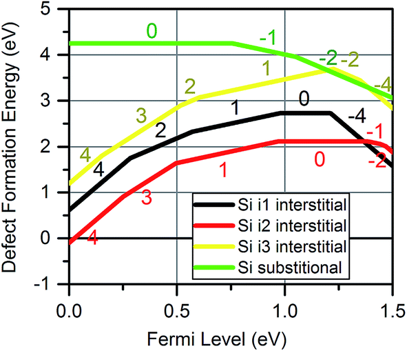 | ||
| Fig. 8 Defect formation energies for silicon defects inside MoO3 at the three sites at a temperature of 300 K and pO2 of 0.2 atm. The charges of the dominant charge states are labelled. | ||
To investigate the accommodation of Si in MoO3 under different processing conditions, Brouwer diagrams were constructed with silicon defects included, presented in Fig. 9. The Brouwer diagrams show that at high temperature and low pO2, silicon is highly soluble in MoO3, and that the preferential presence of Sii defects prevents the formation of VMo, which were observed in trace amounts in the intrinsic Brouwer diagrams. The SiMo defects do not appear under the conditions shown. At all temperatures and pressures, Sii are more abundant than Moi, in fact at all pressures below atmospheric conditions,  are the second most prevalent defects after
  , although the concentrations are not impactful until low pO2. Si interstitials are primarily charge neutral, with some +1 and −1 defects also occurring in roughly equal quantities at low pO2.
 | ||
| Fig. 9 Brouwer diagrams showing the defect concentrations per formula unit as a function of temperature at constant pressure of (a) 0.2 atm and (b) 10−8 atm, and as a function of partial pressure at constant temperatures of (c) 500 K and (d) 700 K. Graphs also include concentrations of electrons and holes and the degree of sub-stoichiometry (x in MoO3−x). The different charge states of each defect type are labelled. | ||
These results imply there might be some concern about silicon contamination. Fig. 10 shows the predicted silicon defect concentration as a function of both pO2 and T, indicating that high amounts of contamination may occur under low pO2 and high T conditions. The thermal evaporation process is often performed at pressures below 10−9 atm,21,92 and a crystallisation anneal performed with a temperature of 700 K in an N2 or Argon ambient with pO2 of 10−6 atm is predicted to produce a silicon defect concentration of 1.3 ppm (or 2.5 × 1017 cm−3). These conditions are similar to what is reported in the literature,20,34 with pO2 estimated on the assumption of 6N purity gasses, indicating that careful consideration of Si interfusion should be taken into account when preparing MoO3−x, either by limiting the temperature, avoiding low pressures, or by reducing the exposure time (provided the kinetics of Si diffusion are slower than that of MoO3 evaporation).
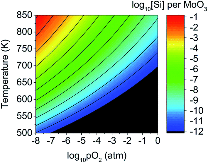 | ||
| Fig. 10 Predicted concentration of silicon interstitial defects as a function of oxygen partial pressure and temperature. Concentrations below 10−12 defects per MoO3 formula unit are in black. | ||
Fig. 11 shows a comparison of the DOS between a defect-free MoO3 supercell and one containing the dominant silicon  defect. The presence of silicon defects introduces a spin-polarised defect state 0.5 eV above the valence band maximum which consequently reduces the bandgap by 0.3 eV. This result suggests that a high amount of silicon penetration would have a significant impact on the electronic properties of the MoO3 layer and hence the performance of any MoO3−x based device. Of particular concern, is the increased parasitic absorption in the MoO3−x contact layers which can directly reduce the energy conversion efficiency of silicon photovoltaic devices.
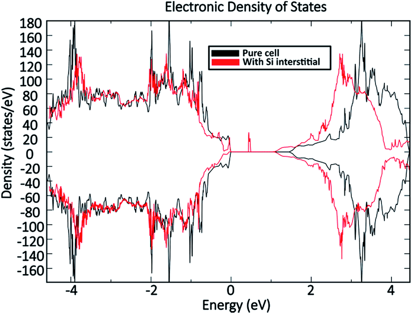 | ||
| Fig. 11 Computed density of states comparison between an MoO3 supercell without defects and an MoO3 supercell containing the dominant silicon interstitial defect. | ||
Conclusion
This study has explored the formation of both intrinsic (oxygen vacancies) and extrinsic (silicon interstitials) in crystalline α-MoO3 under different preparation conditions using ab initio DFT. The results of the simulations are compared with previous studies and it was shown that, despite the axis and bond length properties of all previous works agreeing to within 9% of each other, the estimation of the defect formation energies of oxygen vacancies are highly inconsistent with each other. In order to rationalise these differences, a rigorous method for calculating formation energies was established, using an unconventional 2 × 2 × 3 supercell to minimise the electrostatic self-interaction between charged defects. All intrinsic defects were simulated, including the molybdenum and oxygen interstitials which had not been considered previously, and their formation energies were calculated as a function of the Fermi level. The calculated formation energies were then used to produce Brouwer diagrams that showed how the concentration of intrinsic defects varied with changing oxygen partial pressure and temperature. It was predicted (from the Brouwer diagrams) that the charge neutral oxygen vacancy is the most dominant intrinsic defect under the range of conditions considered, but other defects such as molybdenum interstitials could also be present at low pO2 and high temperatures. Furthermore, it was shown that the stoichiometry of the MoO3−x varied as a simple function of pO2 and temperature. These findings can help explain previous experimental results in terms of the effect of preparation conditions on material properties.The methods used for intrinsic defects were then extended to silicon defects in MoO3. It was found that silicon is most readily incorporated as an interstitial species, where it introduces a spin-polarised defect state 0.5 eV above the MoO3 valence band maximum and consequently reduces the bandgap of the metal oxide by 0.3 eV. The silicon defect can reach a concentration of 1.3 ppm at commonly-used processing conditions of 700 K and 10−6 atm oxygen partial pressure, and significantly higher concentrations at lower pO2 and/or higher temperatures. This result suggests that silicon contamination of MoO3−x contact layers may represent a serious durability issue for silicon PV cells and modules and may impact device performance due to increased parasitic absorption.
The DFT method outlined in this paper could also be extended to other foreign defects such as hydrogen, which may be of particular interest for silicon solar cells as hydrogen can reduce interface state densities at a crystalline silicon surface. Further modelling could also determine the electronic effects of specific oxygen vacancy defect clusters in this material. The Brouwer diagrams developed through this study could be used to optimise fabrication processes to achieve a target stoichiometry and/or defect concentration. Since the defects have significant effects on material properties, this tuning could have a large effect on the viability of crystalline MoO3−x contacts and hence the development and advancement of efficient and cost-effective MoO3−x-based devices.
Conflicts of interest
There are no conflicts of interest to declare.Acknowledgements
The authors would like to thanks Dr Tahini for his help and insightful suggestions. This research was undertaken with the assistance of resources and services from the National Computational Infrastructure (NCI), which is supported by the Australian Government, and the Multi-modal Australian ScienceS Imaging and Visualisation Environment (MASSIVE) (http://www.massive.org.au). Access to computational resources was granted through the national merit allocation scheme (NCMAS) and UNSW's “HCP@NCI” trial scheme. Daniel Lambert acknowledges the support of the Australian Government through the award of a Research Training Program (RTP) scholarship. P. A. B. acknowledges the Tyree Foundation and the Australian Nuclear Science and Technology Organisation for financial support.Notes and references
- S. H. Lee, Y. H. Kim, R. Deshpande, P. A. Parilla, E. Whitney, D. T. Gillaspie, K. M. Jones, A. Mahan, S. Zhang and A. C. Dillon, Adv. Mater., 2008, 20, 3627–3632 CrossRef CAS.
- M. B. Sreedhara, A. L. Santhosha, A. J. Bhattacharyya and C. N. R. Rao, J. Mater. Chem. A, 2016, 4, 9466–9471 CAS.
- F. Li, C. R. Cabrera and Z. Chen, J. Mater. Chem. A, 2014, 2, 19180–19188 CAS.
- Q.-L. Lu, S.-X. Zhao, C.-K. Chen, X. Wang, Y.-F. Deng and C.-W. Nan, J. Mater. Chem. A, 2016, 4, 14560–14566 CAS.
- H. Peng, G. Ma, J. Mu, K. Sun and Z. Lei, J. Mater. Chem. A, 2014, 2, 10384–10388 CAS.
- T. Brezesinski, J. Wang, S. H. Tolbert and B. Dunn, Nat. Mater., 2010, 9, 146 CrossRef CAS PubMed.
- Z. Ouyang, S. N. Lou, D. Lau, J. Chen, S. Lim, P.-C. Hsiao, D.-W. Wang, R. Amal, Y. H. Ng and A. Lennon, Adv. Energy Mater., 2017, 7, 1602325 CrossRef.
- V. Augustyn, P. Simon and B. Dunn, Energy Environ. Sci., 2014, 7, 1597–1614 CAS.
- K. Galatsis, Y. Li, W. Wlodarski, E. Comini, G. Faglia and G. Sberveglieri, Sens. Actuators, B, 2001, 77, 472–477 CrossRef CAS.
- M. B. Rahmani, S.-H. Keshmiri, J. Yu, A. Sadek, L. Al-Mashat, A. Moafi, K. Latham, Y. Li, W. Wlodarski and K. Kalantar-Zadeh, Sens. Actuators, B, 2010, 145, 13–19 CrossRef CAS.
- P. L. Gai-Boyes, Catal. Rev.: Sci. Eng., 1992, 34, 1–54 CAS.
- J. Haber and E. Lalik, Catal. Today, 1997, 33, 119–137 CrossRef CAS.
- J. B. Wagner, S. B. Abd Hamid, D. Othman, O. Timpe, S. Knobl, D. Niemeyer, D. S. Su and R. Schlögl, J. Catal., 2004, 225, 78–85 CrossRef CAS.
- S. N. Lou, Y. H. Ng, C. Ng, J. Scott and R. Amal, ChemSusChem, 2014, 7, 1934–1941 CrossRef CAS PubMed.
- S. N. Lou, N. Yap, J. Scott, R. Amal and Y. H. Ng, Sci. Rep., 2014, 4, 7428 CrossRef CAS PubMed.
- A. Guerfi, R. Paynter and L. H. Dao, J. Electrochem. Soc., 1995, 142, 3457–3464 CrossRef CAS.
- T. C. Arnoldussen, J. Electrochem. Soc., 1976, 123, 527–531 CrossRef CAS.
- J. Yao, B. Loo and A. Fujishima, Ber. Bunsen-Ges., 1990, 94, 13–17 CrossRef CAS.
- S. Chen, X. Yu, M. Zhang, J. Cao, Y. Li, L. Ding and G. Shi, J. Mater. Chem. A, 2015, 3, 18380–18383 CAS.
- C. Battaglia, X. Yin, M. Zheng, I. D. Sharp, T. Chen, S. McDonnell, A. Azcatl, C. Carraro, B. Ma and R. Maboudian, Nano Lett., 2014, 14, 967–971 CrossRef CAS PubMed.
- J. Bullock, A. Cuevas, T. Allen and C. Battaglia, Appl. Phys. Lett., 2014, 105, 232109 CrossRef.
- C. Battaglia, S. M. De Nicolas, S. De Wolf, X. Yin, M. Zheng, C. Ballif and A. Javey, Appl. Phys. Lett., 2014, 104, 113902 CrossRef.
- X. Fan, M. Zhang, X. Wang, F. Yang and X. Meng, J. Mater. Chem. A, 2013, 1, 8694–8709 CAS.
- J. Meyer, S. Hamwi, M. Kröger, W. Kowalsky, T. Riedl and A. Kahn, Adv. Mater., 2012, 24, 5408–5427 CrossRef CAS PubMed.
- C. Girotto, E. Voroshazi, D. Cheyns, P. Heremans and B. P. Rand, ACS Appl. Mater. Interfaces, 2011, 3, 3244–3247 CAS.
- S. Ranjbar, G. Brammertz, B. Vermang, A. Hadipour, S. Cong, K. Suganuma, T. Schnabel, M. Meuris, A. da Cunha and J. Poortmans, Phys. Status Solidi A, 2017, 214, 1600534 CrossRef.
- K. Zilberberg and T. Riedl, J. Mater. Chem. A, 2016, 4, 14481–14508 CAS.
- M. Acik and S. B. Darling, J. Mater. Chem. A, 2016, 4, 6185–6235 CAS.
- C.-W. Chen, S.-Y. Hsiao, C.-Y. Chen, H.-W. Kang, Z.-Y. Huang and H.-W. Lin, J. Mater. Chem. A, 2015, 3, 9152–9159 CAS.
- Y. Zhao, A. M. Nardes and K. Zhu, Appl. Phys. Lett., 2014, 104, 213906 CrossRef.
- J. Geissbühler, J. Werner, S. M. de Nicolas, L. Barraud, A. Hessler-Wyser, M. Despeisse, S. Nicolay, A. Tomasi, B. Niesen and S. De Wolf, Appl. Phys. Lett., 2015, 107, 081601 CrossRef.
- M. Taguchi, A. Yano, S. Tohoda, K. Matsuyama, Y. Nakamura, T. Nishiwaki, K. Fujita and E. Maruyama, IEEE J. Photovolt., 2014, 4, 96–99 CrossRef.
- A. L. F. Cauduro, R. dos Reis, G. Chen, A. K. Schmid, C. Méthivier, H.-G. Rubahn, L. Bossard-Giannesini, H. Cruguel, N. Witkowski and M. Madsen, ACS Appl. Mater. Interfaces, 2017, 9, 7717–7724 Search PubMed.
- M. Sook Oh, B. Seob Yang, J. Ho Lee, S. Ha Oh, U. Soo Lee, Y. Jang Kim, H. Joon Kim and M. Soo Huh, J. Vac. Sci. Technol., A, 2012, 30, 031501 Search PubMed.
- M. T. Greiner, L. Chai, M. G. Helander, W. M. Tang and Z. H. Lu, Adv. Funct. Mater., 2012, 22, 4557–4568 CrossRef CAS.
- A. Bouzidi, N. Benramdane, H. Tabet-Derraz, C. Mathieu, B. Khelifa and R. Desfeux, Mater. Sci. Eng., B, 2003, 97, 5–8 CrossRef.
- A. L. F. Cauduro, Z. E. Fabrim, M. Ahmadpour, P. F. Fichtner, S. Hassing, H.-G. Rubahn and M. Madsen, Appl. Phys. Lett., 2015, 106, 202101 CrossRef.
- K. Kanai, K. Koizumi, S. Ouchi, Y. Tsukamoto, K. Sakanoue, Y. Ouchi and K. Seki, Org. Electron., 2010, 11, 188–194 CrossRef CAS.
- K. Eda, J. Solid State Chem., 1991, 95, 64–73 CrossRef CAS.
- S. Deb and J. Chopoorian, J. Appl. Phys., 1966, 37, 4818–4825 CrossRef CAS.
- Y. Li, D. Wang, Q. An, B. Ren, Y. Rong and Y. Yao, J. Mater. Chem. A, 2016, 4, 5402–5405 CAS.
- S. Balendhran, J. Deng, J. Z. Ou, S. Walia, J. Scott, J. Tang, K. L. Wang, M. R. Field, S. Russo and S. Zhuiykov, Adv. Mater., 2013, 25, 109–114 CrossRef CAS PubMed.
- S. Balendhran, S. Walia, H. Nili, J. Z. Ou, S. Zhuiykov, R. B. Kaner, S. Sriram, M. Bhaskaran and K. Kalantar-zadeh, Adv. Funct. Mater., 2013, 23, 3952–3970 CrossRef CAS.
- C. Julien, A. Khelfa, O. Hussain and G. Nazri, J. Cryst. Growth, 1995, 156, 235–244 CrossRef CAS.
- M. Dieterle, G. Weinberg and G. Mestl, Phys. Chem. Chem. Phys., 2002, 4, 812–821 RSC.
- H.-S. Kim, J. B. Cook, H. Lin, J. S. Ko, S. H. Tolbert, V. Ozolins and B. Dunn, Nat. Mater., 2016, 16, 454–460 CrossRef PubMed.
- H. A. Tahini, X. Tan, S. N. Lou, J. Scott, R. Amal, Y. H. Ng and S. C. Smith, ACS Appl. Mater. Interfaces, 2016, 8, 10911–10917 CAS.
- S. O. Akande, A. Chroneos, M. Vasilopoulou, S. Kennou and U. Schwingenschlögl, J. Mater. Chem. C, 2016, 9526–9521 RSC.
- Y. Guo and J. Robertson, Appl. Phys. Lett., 2014, 105, 222110 CrossRef.
- M. Anwar and C. Hogarth, J. Mater. Sci., 1990, 25, 4918–4928 CrossRef CAS.
- M. Baldoni, L. Craco, G. Seifert and S. Leoni, J. Mater. Chem. A, 2013, 1, 1778–1784 CAS.
- Y.-H. Lei and Z.-X. Chen, J. Phys. Chem. C, 2012, 116, 25757–25764 CAS.
- X. Sha, L. Chen, A. C. Cooper, G. P. Pez and H. Cheng, J. Phys. Chem. C, 2009, 113, 11399–11407 CAS.
- J. Handzlik and J. Ogonowski, J. Phys. Chem. C, 2012, 116, 5571–5584 CAS.
- R. Radhakrishnan, C. Reed, S. Oyama, M. Seman, J. Kondo, K. Domen, Y. Ohminami and K. Asakura, J. Phys. Chem. B, 2001, 105, 8519–8530 CrossRef CAS.
- S. Chempath, Y. Zhang and A. T. Bell, J. Phys. Chem. C, 2007, 111, 1291–1298 CAS.
- G. Kresse and J. Furthmüller, Phys. Rev. B: Condens. Matter Mater. Phys., 1996, 54, 11169 CrossRef CAS.
- J. P. Perdew, K. Burke and M. Ernzerhof, Phys. Rev. Lett., 1996, 77, 3865 CrossRef CAS PubMed.
- S. Dudarev, G. Botton, S. Savrasov, C. Humphreys and A. Sutton, Phys. Rev. B: Condens. Matter Mater. Phys., 1998, 57, 1505 CrossRef CAS.
- R. Coquet and D. J. Willock, Phys. Chem. Chem. Phys., 2005, 7, 3819–3828 RSC.
- D. O. Scanlon, G. W. Watson, D. Payne, G. Atkinson, R. Egdell and D. Law, J. Phys. Chem. C, 2010, 114, 4636–4645 CAS.
- S. Grimme, J. Antony, S. Ehrlich and H. Krieg, J. Chem. Phys., 2010, 132, 154104 CrossRef PubMed.
- N. D. M. Hine, K. Frensch, W. M. C. Foulkes and M. W. Finnis, Phys. Rev. B: Condens. Matter Mater. Phys., 2009, 79, 024112 CrossRef.
- M. Finnis, A. Lozovoi and A. Alavi, Annu. Rev. Mater. Res., 2005, 35, 167–207 CrossRef CAS.
- P. J. Linstrom and W. Mallard, in NIST Chemistry webbook; NIST standard reference database No. 69, 2001 Search PubMed.
- S. T. Murphy and N. D. Hine, Phys. Rev. B: Condens. Matter Mater. Phys., 2013, 87, 094111 CrossRef.
- R. Rurali and X. Cartoixà, Nano Lett., 2009, 9, 975–979 CrossRef CAS PubMed.
- F. Kröger and H. Vink, Solid State Phys., 1956, 3, 307–435 Search PubMed.
- S. Lany and A. Zunger, Phys. Rev. B: Condens. Matter Mater. Phys., 2008, 78, 235104 CrossRef.
- S. Lany and A. Zunger, Modell. Simul. Mater. Sci. Eng., 2009, 17, 084002 CrossRef.
- C. Varvenne, F. Bruneval, M.-C. Marinica and E. Clouet, Phys. Rev. B: Condens. Matter Mater. Phys., 2013, 88, 134102 CrossRef.
- P. A. Burr and M. W. D. Cooper, Phys. Rev. B, 2017, 96, 094107 CrossRef.
- L. Lajaunie, F. Boucher, R. Dessapt and P. Moreau, Phys. Rev. B: Condens. Matter Mater. Phys., 2013, 88, 115141 CrossRef.
- J. Du, V. Anye, E. Vodah, T. Tong, M. Zebaze Kana and W. Soboyejo, J. Appl. Phys., 2014, 115, 233703 CrossRef.
- R. Hill, Proc. Phys. Soc., London, Sect. A, 1952, 65, 349 CrossRef.
- S. T. Murphy and N. D. Hine, Chem. Mater., 2014, 26, 1629–1638 CrossRef CAS.
- L. Kihlborg, Ark. Kemi, 1963, 21, 357 CAS.
- R. Coquet and D. J. Willock, Phys. Chem. Chem. Phys., 2005, 7, 3819–3828 RSC.
- P.-R. Huang, Y. He, C. Cao and Z.-H. Lu, Sci. Rep., 2014, 4, 7131 CrossRef CAS PubMed.
- S. Grimme, J. Comput. Chem., 2006, 27, 1787–1799 CrossRef CAS PubMed.
- J. Klimeš, D. R. Bowler and A. Michaelides, Phys. Rev. B: Condens. Matter Mater. Phys., 2011, 83, 195131 CrossRef.
- H. Ding, K. G. Ray, V. Ozolins and M. Asta, Phys. Rev. B: Condens. Matter Mater. Phys., 2012, 85, 012104 CrossRef.
- V. Agarwal and H. Metiu, J. Phys. Chem. C, 2016, 120, 19252–19264 CAS.
- M. Kroger, S. Hamwi, J. Meyer, T. Riedl, W. Kowalsky and A. Kahn, Appl. Phys. Lett., 2009, 95, 123301 CrossRef.
- H. Peelaers and C. G. Van de Walle, J. Phys.: Condens. Matter, 2014, 26, 305502 CrossRef CAS PubMed.
- E. Sanville, S. D. Kenny, R. Smith and G. Henkelman, J. Comput. Chem., 2007, 28, 899–908 CrossRef CAS PubMed.
- D. Rutkowska-Zbik, R. Grybos and R. Tokarz-Sobieraj, Struct. Chem., 2012, 23, 1417–1424 CrossRef CAS.
- A. H. Reshak, RSC Adv., 2015, 5, 22044–22052 RSC.
- S. K. Deb, Proc. R. Soc. London, Ser. A, 1968, 304, 211–231 CrossRef.
- M. T. Greiner and Z.-H. Lu, NPG Asia Mater., 2013, 5, e55 CrossRef CAS.
- T. S. Sian and G. Reddy, Sol. Energy Mater. Sol. Cells, 2004, 82, 375–386 CrossRef CAS.
- S. Chuang, C. Battaglia, A. Azcatl, S. McDonnell, J. S. Kang, X. Yin, M. Tosun, R. Kapadia, H. Fang and R. M. Wallace, Nano Lett., 2014, 14, 1337–1342 CrossRef CAS PubMed.
| This journal is © The Royal Society of Chemistry 2017 |