
 Open Access Article
 This Open Access Article is licensed under a
 Creative Commons Attribution 3.0 Unported Licence
Role of nanoparticle surface defects in the conduction mechanism of polymer–nanoparticle electrical bistable devices
Jiaping Song,
Huizhen Han,
Bo Peng,
Yufeng Hu *,
Qiuhong Cui,
Zhidong Lou,
Yanbing Hou and
Feng Teng*
*,
Qiuhong Cui,
Zhidong Lou,
Yanbing Hou and
Feng Teng*
Key Laboratory of Luminescence and Optical Information, Ministry of Education, Beijing Jiaotong University, Beijing 100044, China. E-mail: yfhu@bjtu.edu.cn; fteng@bjtu.edu.cn; Tel: +86 10 5168 4860
First published on 24th November 2017
Abstract
Polymer/nanoparticle (NP) composite films have attracted great attention due to their potential applications in electrical bistable devices. The bistable mechanism is usually attributed to electron trapping and detrapping between the NP trap center and the polymer matrix. However, the exact conduction switching mechanism is still in controversy and even in the same polymer/NP system based devices the switch-on mechanism has been explained by two different models: either Fowler–Nordheim (FN) tunneling or trapped charge-limit-current (TCLC). Therefore, the study on the conduction switching mechanism for polymer/NP composite electrical bistable devices is critically necessary. In this work, ZnO NPs embedded in poly (ethylene oxide) (PEO) were first applied in electrical bistable devices using a solution process and the effect of the nanoparticle surface defects on the conduction switching mechanism is studied. The electrical bistability is observed from the device with the structure ITO/PEO![[thin space (1/6-em)]](https://www.rsc.org/images/entities/char_2009.gif) :ZnO-NPs/Al and the conduction switch-on process is dependent on the existence of ZnO surface defects. The effect of the nanoparticle surface defects was investigated by current–voltage, Scanning Electron Microscopy (SEM), and photoluminescence measurements. Besides effectively separating nanoparticles, the surface capping can passivate the surface defects and affect the electrical hysteresis. The switch-on mechanism for the devices based on the NPs with surface detects can be modeled by TCLC while the one based on the NPs with the complete surface defect passivation can be explained by FN tunneling. The results demonstrate that the FN tunneling induced conduction switch-on process is more desirable in electrical bistable devices due to the better device performances.
:ZnO-NPs/Al and the conduction switch-on process is dependent on the existence of ZnO surface defects. The effect of the nanoparticle surface defects was investigated by current–voltage, Scanning Electron Microscopy (SEM), and photoluminescence measurements. Besides effectively separating nanoparticles, the surface capping can passivate the surface defects and affect the electrical hysteresis. The switch-on mechanism for the devices based on the NPs with surface detects can be modeled by TCLC while the one based on the NPs with the complete surface defect passivation can be explained by FN tunneling. The results demonstrate that the FN tunneling induced conduction switch-on process is more desirable in electrical bistable devices due to the better device performances.
1. Introduction
Polymer–nanoparticle (NP) hybrid electrical bistable devices have been studied extensively during recent years1–4 because of their unique advantages, such as: low cost, simple-fabrication process, and high mechanical flexibility.5 The polymers are mainly divided into two categories. One is the semiconductor polymer, such as poly-[2-methoxy-5-(2′-ethyl-hexyloxy)-1,4-phenylenevinylene] (MEH-PPV),6 poly(N-vinylcarbazole) (PVK),1,7,8 and poly(3-hexylthiophene) (P3HT).9 The other is the dielectric polymer, for instance, poly(methyl methacrylate) (PMMA),10 poly(vinyl alcohol) (PVA),11,12 polyimide (PI),13 and polyvinylpyrrolidone (PVP).14,15 Compared with the semiconductor polymer, the dielectric polymer has several advantages:2 (1) the larger bandgap induced higher barrier is beneficial to the tunneling process which is preferred in the electrical bistable device. (2) The active layer has good chemical/thermal stability. (3) The material has a lower cost. To date, various nanoparticles (NPs) have been widely reported to form polymer–nanoparticle bistable devices such as Ag,2 Ag2S,16 or CdSe/ZnS.8 Herein, the nanoparticles act as charge trapping–detrapping centers, leading to a stable performance and good reproducibility of the devices. Among these inorganic nanoparticles, ZnO has attracted intense attention due to its chemical/optical stability and low toxicity. When using nanoparticles, capping with a traditional surfactant such as dodecanethiol,17 oleylamine,18 and oleic acid19 etc. has been necessarily used to prevent the aggregation of nanoparticles. Recently, the hybrid electrical bistable devices based on the nanocomposite of ZnO nanoparticles and the dielectric polymer (PMMA, PVP, and PI)13,15,20 have been demonstrated. The relevant conduction switch-on mechanisms are still unclear and mostly explained by the two models: Fowler–Nordheim (FN) tunneling and trapped charge-limit-current (TCLC), even in the same material system, such as ZnO/PMMA.21–23 Therefore, it is quite necessary to carefully analyze the underlying mechanism of the electrical bistable device based on the ZnO NPs and dielectric polymer composites.On the other hand, it has been widely studied that the nanoparticle surface defect passivation with surfactants is efficient to improve device performances of metal oxide nanoparticles based hybrid solar cells24,25 since the surface defect can easily trap the photo-excited electrons, which weakens the series resistance. In the electrical bistable devices, the nanoparticles act as charge trapping–detrapping centers, therefore, the surface defect would affect the conduction switch-on process. However, the nanoparticle surface defect has been barely investigated in polymer–nanoparticle bistable devices. Recently, a popular dielectric polymer, poly(ethylene oxide) (PEO),26 has been performed to cap ZnO nanoparticles by sharing the lone electron pair of oxygen24 since they can passivate the surface defects of nanoparticles and inhibit the nanoparticle aggregation. Therefore, PEO might be promising for electrical bistable devices since it can play both roles of the matrix material and passivation material at the same time. Therefore, a good morphology without a serious nanoparticle aggregation can be obtained in both films based on PEO:ZnO nanocomposite with and without traditional surfactant. This offers us an opportunity to understand the role of the nanoparticle surface defects on the electrical bistable devices. In this work, the PEO:ZnO-NP nanocomposite electrical bistable devices were fabricated through spin-coating on indium tin oxide (ITO) coated substrates to study the effect of ZnO nanoparticle surface defects on PEO:ZnO bistable devices. The micro-structures of the devices were studied by Scanning Electron Microscope (SEM) images and the device working mechanism is proposed with the help of the photoluminescence (PL) spectrum and current–voltage (I–V) measurements.
2. Experimental details
The ZnO nanoparticles without surfactant in this study were synthesized following the reported method.27 2.95 g zinc acetate dihydrate [Zn(AC)2] was dissolved in 125 mL methanol and 1.48 g KOH was dissolved in 65 mL methanol. Then, the KOH solution was mixed with the Zn(AC)2 solution at 60 °C under vigorous stirring for 3 hours, followed by a 5 hour precipitation process in which the ZnO nanoparticles precipitated. Afterwards, the ZnO nanoparticles were washed twice with methanol by centrifugation of the dispersion and thus were dissolved in chlorobenzene to form a 35 mg mL−1 ZnO solution. The X-ray diffraction pattern (XRD) shown in Fig. 1(a) indicates that the nanoparticle is hexagonal wurtzite-type ZnO. Finally, PEO with a molecular weight of 100000 was dissolved in chlorobenzene and then the PEO solution was mixed with ZnO nanoparticles in a chlorobenzene and methanol (1:1, volume ratio) hybrid solution at different mass ratios with a constant PEO concentration of 25 mg mL−1. The ZnO NP (with surfactant) ethanol dispersion was purchased from Sigma company and was mixed with the PEO chlorobenzene solution to achieve PEO/ZnO-NPs chlorobenzene and ethanol (1:1, volume ratio) hybrid solution at various PEO:ZnO mass ratios.
 | ||
| Fig. 1 (a) XRD pattern of ZnO nanoparticles with standard diffraction lines of monoclinic ZnO; (b) schematic diagram of the ITO/PEO:ZnO/Al bistable devices; (c) PL spectra of PEO capped ZnO nanoparticles on top of glass; (d) I–V curves of the organic bistable devices with the various PEO:ZnO ratios under 5 V sweep voltage. | ||
The indium tin oxide (ITO) conducting glass substrates with a sheet resistance of 10 Ω sq−1 were cleaned with detergent and sonicated with deionized water and ethanol for 30 minutes, and then were dried by nitrogen flow and treated in ultraviolet ozone before spin coating. Afterwards, the PEO/ZnO hybrid solution was spin-coated onto the pre-cleaned ITO substrates with 3000 rpm for 40 s and the fabricated films were baked on a hot-plate at 60 °C for 20 min to dry the solvent. Finally, the 100 nm Al electrode was thermally evaporated on top of the active film through a shadow mask under the vacuum of about 1 × 10⁶ torr. Therefore, the fabricated device has a structure of ITO/PEO:ZnO/Al as shown in the schematic diagram in Fig. 1(b).
3. Results and discussion
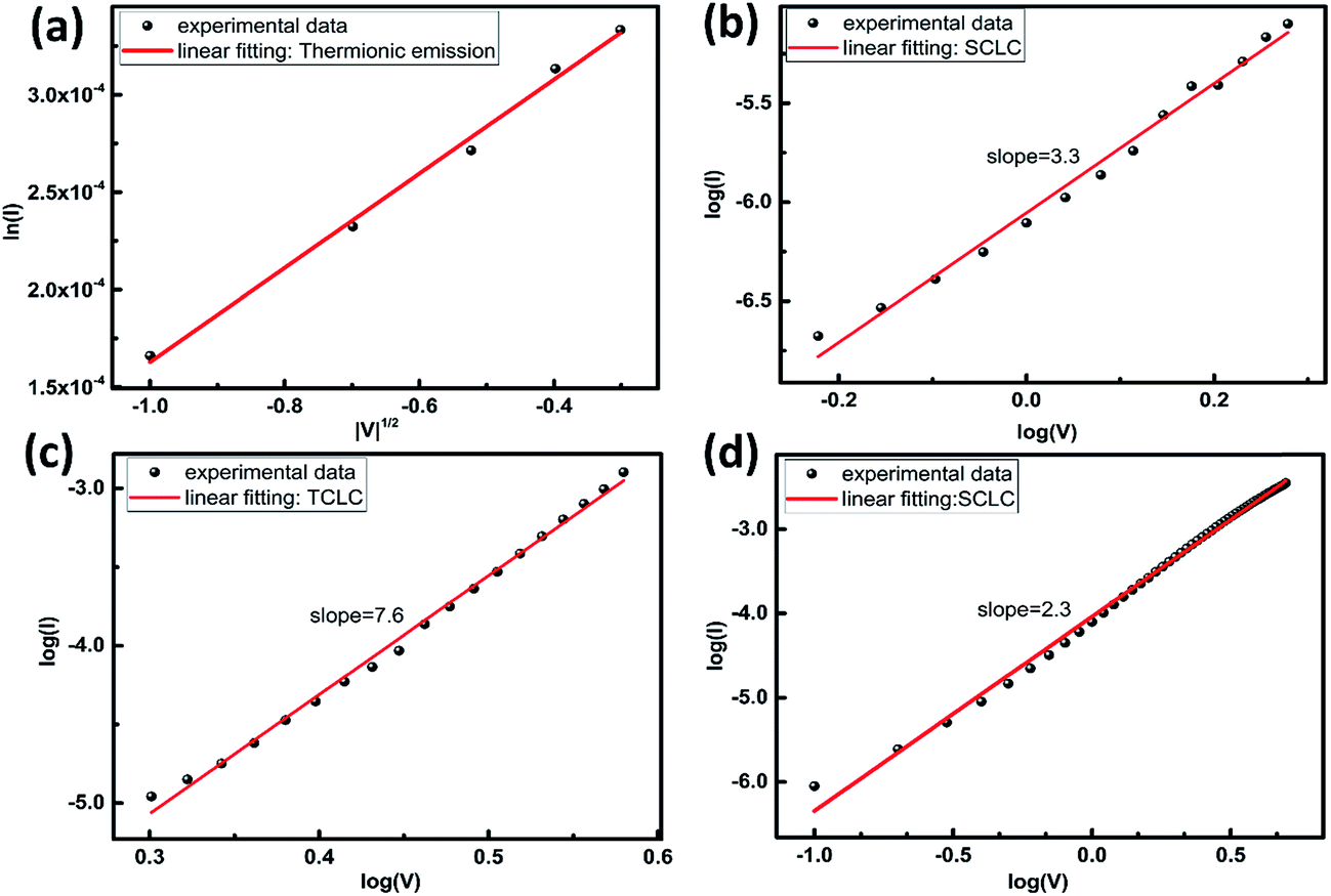
As demonstrated in the previous studies PEO can passivate the surface defects of ZnO nanoparticles by sharing the lone electron pair of oxygen.24 The PL spectra of the various devices based on different PEO:ZnO ratios (5:1, 10:1, 20:1, 30:1 and pure ZnO) were measured to study the capping effect of PEO on ZnO-NPs. As shown in Fig. 1(c), two emission peaks are observed with the 300 nm excitation wavelength. The weak peak at about 355 nm is attributed to the edge emission of ZnO (bulk emission), while the intense broad emission at around 520 nm is assigned to the deep emission, arising from the impurities or lattice imperfections of ZnO.28 Fig. 1(c) shows that the deep emission intensity of the PEO capped ZnO films decreased comparing with the one of the pristine ZnO film, indicating that PEO can passivate the surface defects of ZnO nanoparticles. It should be noted that even when the PEO:ZnO ratio is as high as 30:1 the surface defect induced deep emission is still much stronger than the bulk emission of ZnO-NPs. This implies that the surface defects cannot be eliminated in this case.
The I–V measurement was conducted with Keithley 2612 voltage source equipment controlled by a computer (Test Script Builder) at room temperature. The sweep voltage was applied between the top Al and the bottom ITO electrodes (Fig. 1(b)) and sequentially scanned from 0 V to −5 V, −5 V to 5 V and 5 V to 0 V. Thus, the different conduction switch characteristics (Fig. 1(d)) were obtained from the various devices: ITO/PEO:ZnO (5:1, 10:1, 20:1 and 30:1)/Al. Either the pure PEO device or the pure ZnO-NP device does not exhibit bistable behavior in the I–V measurement while the former has a lower electrical current and the latter has a higher electrical current due to their different conductivities (data not shown). When the PEO:ZnO ratio is as low as 5:1, the device shows a significantly high current during the whole sweep process without any hysteresis behavior which is almost same as the characteristic of the pure ZnO-NP device. This is reasonable since the active layer contains a large amount of ZnO NPs which form clusters connected with the neighboring ones. When the PEO:ZnO ratio increase to 10:1 and 20:1, both devices exhibit a larger ON/OFF ratio with a typical current hysteresis: a high-conducting state (ON state) and a low-conducting state (OFF state) under voltage scan. When the PEO:ZnO ratio is increased to 30:1, the device exhibits a much lower current during the whole sweep process with a quite poor hysteresis behavior most likely because the ZnO NPs are well separated from each other in the PEO matrix, which suggests that the high concentration of PEO in the active layer can impede the device electric behavior since PEO is insulating.
The above discussion is supported by the topographies of the PEO:ZnO films which are depicted by the SEM images in Fig. 2. The results reveal that the surface morphology of the pristine ZnO film exhibits a rough cluster structure (Fig. 2(a)) and appears different after adding various amounts of PEO. Fig. 2(b) implies that PEO can cap the grain boundary and smooth the surface of the ZnO nanoparticle film. With increasing the amount of PEO (Fig. 2(c and d)), a smoother surface can be observed and the grained surface of the ZnO film has been partially covered by the PEO surface.
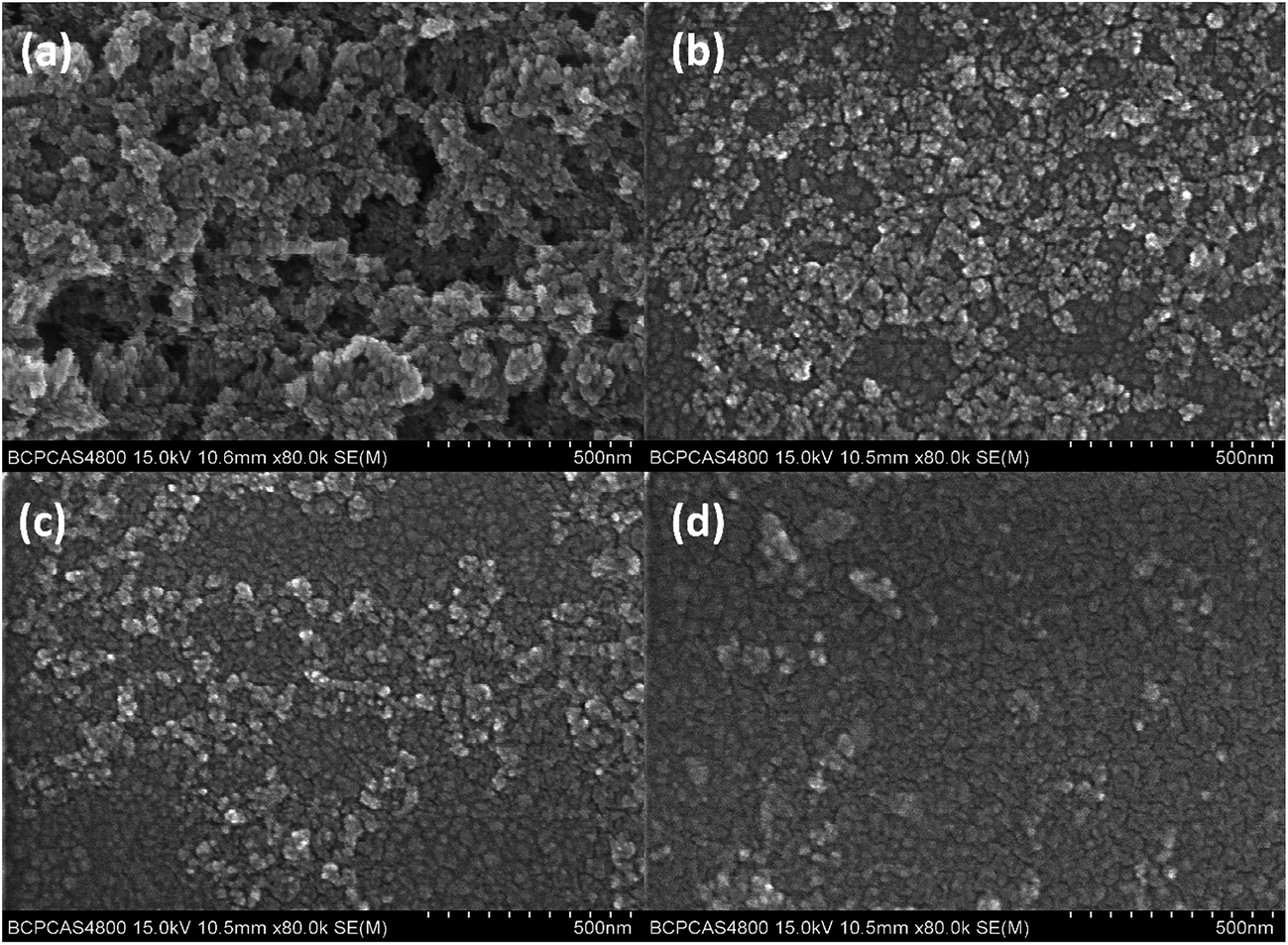 | ||
| Fig. 2 SEM images of PEO:ZnO film with different mass ratios: (a) ZnO only, (b) 5:1, (c) 10:1, (d) 20:1. | ||
The experimental I–V curves of the devices based on different PEO:ZnO mass ratios of 10:1 and 20:1 (shown in Fig. 1(d)) were fitted by several theoretical models to analyze the carrier transport mechanism. The theoretical I–V curve linear filling results of the two devices are consistent and the result of the device based on 10:1 is shown in Fig. 3. In the OFF state for the negative region below −0.5 V (Fig. 3(a)), the data can be well fitted with the thermionic emission using the following equation:15
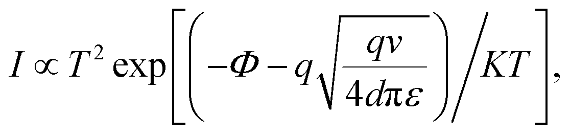 I–logV characteristic in the voltage from −0.6 V to −1.9 V shown in Fig. 3(b) exhibits a linear slope of 3.3, which conforms to a dominant SCLC model for the ideal case. The result suggests that the captured electrons by the interface traps can act as space charges, as has previously been reported.30,31 For the applied voltage from −2 V to −3.8 V, a larger linear slope of 7.6 is observed in Fig. 3(c) and the response follows a strong SCLC (α ≫ 2), which is specifically called as trapped-charge-limited-current (TCLC) model. This suggests that when the voltage surpasses a threshold voltage, the electrons will be captured by the nanoparticle surface defect induced traps distributed exponentially within the forbidden gap, therefore the electrical current increase rapidly and finally reach ON state. This explanation is reasoned since the previous work demonstrated the TCLC induced significant current enhancement is attributed to the presence of the oxygen vacancy in the ZnO nanorods embedded in PMMA.23 When the applied voltage sweeps from −5 V to −0.1 V, the I–V data can be well fitted with SCLC model with the slope of 2.3 as depicted in Fig. 3(d). This seems that all the traps are fully occupied and the electrons can transport through the device without being trapped, leading to a trap-free SCLC after TCLC.32
 | ||
| Fig. 3 Theoretical linear fitting (solid line) of I–V characteristics in positive voltage region: (a) thermionic emission model plot from −0.1 V to −0.5 V in OFF state, (b) space-charge-limited-current (SCLC) theory plot from −0.6 V to −1.9 V in OFF state, (c) TCLC theory plot from −2 V to −3.8 V in OFF state, (d) SCLC model plot from −5 V to −0.1 V in ON state. | ||
As the above discussed, the presence of the surface defects of the ZnO-NPs plays a key role on the conduction switch-on for the electrical bistable devices based on surfactant-free PEO:ZnO-NPs. Then an interesting question arises: what will occur on the device if the surface defect induced traps are eliminated? One ideal way to answer this question would be to fabricate the device with increasing PEO amount until the surface defect is completely passivated. Unfortunately, the electrical bistability then cannot be observed due to the high resistivity of PEO. Therefore, the ZnO-NPs with traditional surfactant embedded in PEO were introduced into the following experiments. Fig. 4(a) shows the PL spectrum of the surfactant-capped ZnO-NP film with only one emission peak at about 380 nm. It indicates that the surface defects of ZnO nanoparticles are eliminated efficiently.28
 | ||
| Fig. 4 (a) PL spectra of the film of the intrinsic ZnO nanoparticles with surfactant on top of the glass; (b) I–V curves of the organic bistable devices with the various PEO:ZnO ratios under 3 V sweep voltage; (c) thermionic emission model plot from −0.1 V to −0.7 V in OFF state; (d) direct tunneling theory plot from −1 V to −1.9 V in OFF state; (e) Fowler–Nordheim (FN) tunneling theory plot from −2 V to −2.9 V in OFF state; (f) space-charge-limited-current (SCLC) model plot from −3 V to −0.1 V in ON state. | ||
Fig. 4(b) shows the I–V characteristics of the ITO/PEO:ZnO (with surfactant)/Al devices with different mass ratios (1:1, 2:1, 10:1, 20:1). The voltage scan was swept by applying a voltage bias in a cyclical manner from 0 V to −3 V, −3 V to 3 V and 3 V to 0 V. All devices exhibit the similar conduction switch-on behavior, which is quite different comparing with the one shown in Fig. 1(d). There is an electrical hysteresis with different currents of a low-resistance state (ON state) and a high-resistance state (OFF state) at the same applied voltage.33 During the first scan from 0 V to −3 V, the electrical current shows a significant enhancement at about −2 V, indicating the bistable switch of the device from OFF state to ON state. Afterwards, the current maintains the ON state during the opposite bias voltage scan from −3 V to 0 V. It is noted that the relatively less PEO was used, the higher on-state current and the more significant hysteresis were obtained in the devices until the PEO:ZnO ratio of 1:1 reached. Among these devices, the one with the PEO:ZnO ratio of 2:1 shows the best bistability and the ON/OFF current ratio starts to drop when the PEO:ZnO mass ratio decreases to 1:1. This trend is reasoned since PEO is insulating while ZnO is much more conductive.
Fig. 4(c–f) show the experimental data and the theoretical curve fitting in different voltage regions. Compared with the result shown in Fig. 3, the different models are used to explain the conduction switch-on in terms of eqn (1) and (2).15,21,34–36
Direct tunneling
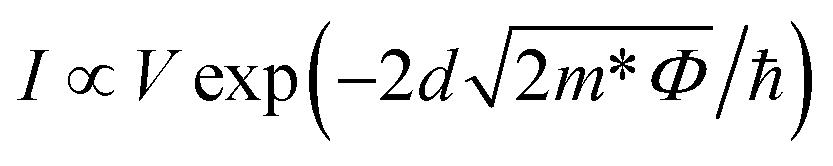 | (1) |
Fowler–Nordheim (FN) tunneling
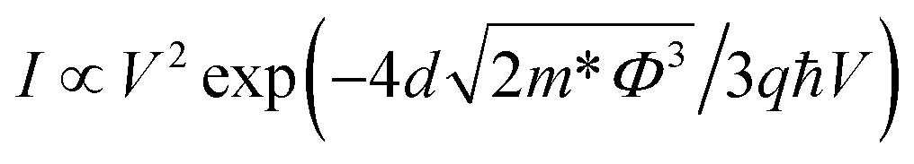 | (2) |
Fig. 4(c) illustrates that the experimental I–V curve is well fitted with thermionic emission model [ln(I) ∝ |V|1/2] from −0.1 V to −0.7 V in the OFF state, indicating that the injected electrons under low voltage are dominated by thermal energy.29 When the applied bias was increased from −1.0 V to −3 V, two distinct current regions are observed and two different models are applied to fit the relevant curves, respectively. Fig. 4(d) shows the direct tunneling model (ln|I/V2| ∝ ln|1/V|) in the low bias region (−1 V to −1.9 V) of the device.35 For the high voltage region (−2 V to −2.9 V), the electron transport can be interpreted as FN tunneling15 as shown in Fig. 4(e). At a low negative bias voltage, electrons are injected into the conduction band of ZnO NPs from ITO electrode due to the defect-free NP surface and some of them can tunnel through PEO matrix through the Al electrode, leading to a direct tunneling.36 With increasing the voltage, the local electrical field induced band bending gradually changes from square to triangular, resulting in a much larger FN tunneling current. The resulting current increases sharply and the electrical state of the device rapidly changes from the OFF state to the ON state. Therefore, in this case, the conduction switch-on is due to FN tunneling with the help of ZnO NP bulks rather than TCLC in the devices shown in Fig. 1(d), in which the NP surface defects play a key role. In the ON state from −3 V to −0.1 V shown in Fig. 4(f), the fitting plot yields a slope of 2.0, which is consistent with SCLC model (I ∝ Vα, α ≈ 2), this indicates that the current injection of the ON state is dominated by the trap-free SCLC model.29
Fig. 5 shows the SEM images of the films with different PEO:ZnO mass ratios. As can be seen, when PEO:ZnO ratio is relatively low (1:1), the homogeneous grain distribution on the film surface attributes to the continuous ZnO NP networks.37 The ZnO NP networks in the film are beneficial to an effective transport of the charge carriers between two electrodes,15 leading to a higher current. However, the ON/OFF ratio is low since the FN tunneling is impeded due to the PEO insulating networks are not formed. With increasing PEO:ZnO ratio, the continuous ZnO NPs could be broken by PEO matrix and the island-like nanoparticles can act as bulk trap centers. Thus, the resulting film morphology can reduce the current of OFF state due to the less conductive of the film and increase the ON/OFF ratio with help of the enhanced FN tunneling. When the ratio of PEO to ZnO NP ratio is larger than 10:1, there are insufficient bulk traps of ZnO NPs in the PEO matrix and the I–V curves for the devices exhibit the smaller ON/OFF current ratios.
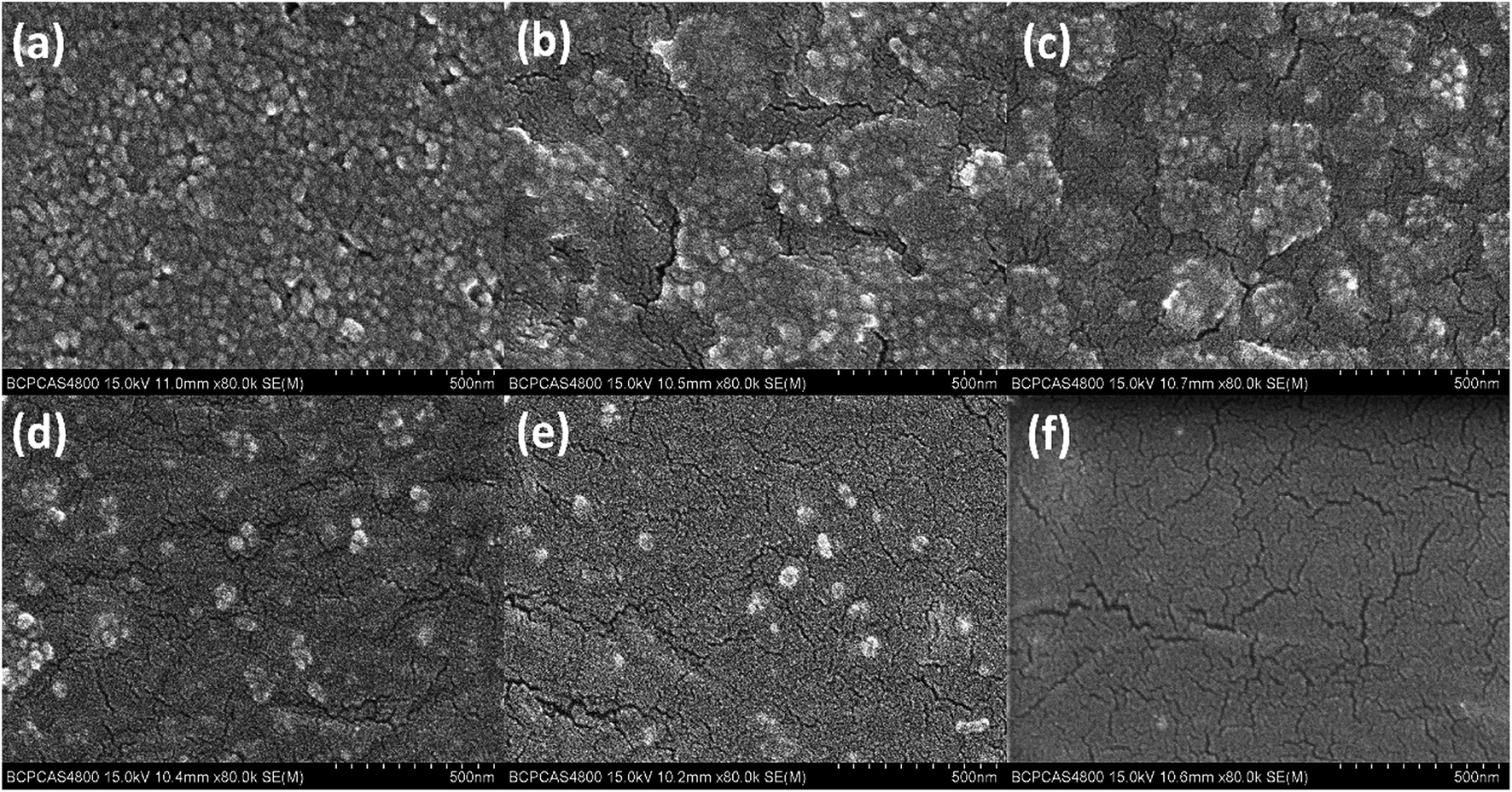 | ||
| Fig. 5 SEM images of PEO:ZnO film with different mass ratio, (a) ZnO only, (b) 1:1, (c) 2:1, (d) 10:1, (e) 20:1, (f) PEO only. | ||
As discussed above, both TCLC and FN tunneling models can be used to explain the conduction switch-on mechanism of the dielectric polymer: ZnO nanocomposite electrical bistable devices. This conclusion is consistent with the previous reports,22 and more importantly, our results demonstrate that the conduction switch-on mechanism strongly depends on the surface defects of the ZnO NPs. The OFF/ON transition of the devices based on ZnO NPs with surface defects can be attributed to the TCLC while the one based on ZnO NPs without surface defects is due to the FN tunneling. In addition, the larger hysteresis behavior and lower operation voltage are obtained in the devices based on the surface defect-free ZnO nanoparticle, indicating that FN tunneling is more desirable for the electrical bistable devices due to the better device performances.
4. Conclusion
The organic bistable device based on PEO/ZnO NP composite was first demonstrated and the physical roles of the nanoparticle surface defects in the device were investigated. All devices show the electrical bistable characteristic and the I–V curves were fitted by different theoretical models in various voltage regions to study the conduction switch-on mechanism. The devices based on ZnO nanoparticles with surface defects exhibit a typical TCLC switch-on while the one without surface defects shows a classic FN tunneling current switch-on. The results demonstrate that the presence of the ZnO NP surface defects can significantly affect the electrical bistable device conduction switch-on process and the device based on the ZnO NPs without surface defects exhibit the better device performances due to the FN tunneling.Conflicts of interest
There are no conflicts to declare.Acknowledgements
This work was supported by National Natural Science Foundation of China (No. 61377028, 61675018, 51603010, 61674012, 61475014, 61475017).References
- R. Kaur, J. Singh and S. K. Tripathi, Incorporation of inorganic nanoparticles into an organic polymer matrix for data storage application, Curr. Appl. Phys., 2017, 17(5), 756–762 CrossRef.
- G. Liu, Z. Jin, Z.-g. Zhang and J. Wang, Realization of nonvolatile organic memory device without using semiconductor, Appl. Phys. Lett., 2014, 104(2), 023303 CrossRef.
- Y. Yang, J. Ouyang, L. Ma, R. J. H. Tseng and C. W. Chu, Electrical Switching and Bistability in Organic/Polymeric Thin Films and Memory Devices, Adv. Funct. Mater., 2006, 16(8), 1001–1014 CrossRef CAS.
- D. Y. Yun, N. S. Arul, D. U. Lee, N. H. Lee and T. W. Kim, Memory stabilities and mechanisms of organic bistable devices with giant memory margins based on Cu2ZnSnS4 nanoparticles/PMMA nanocomposites, Org. Electron., 2015, 320–324 CrossRef CAS.
- D. I. Son, J. H. Kim, D. H. Park, W. K. Choi, F. Li and J. H. Ham, et al., Nonvolatile flexible organic bistable devices fabricated utilizing CdSe/ZnS nanoparticles embedded in a conducting poly N-vinylcarbazole polymer layer, Nanotechnology, 2008, 19, 055204 CrossRef PubMed.
- C. V. V. Ramana, M. K. Moodley, V. Kannan and A. Maity, Solution based-spin cast processed organic bistable memory device, Solid-State Electron., 2013, 81, 45–50 CrossRef CAS.
- E. Zhao, D. Liu, L. Liu, X. Yang, W. Kan and Y. Sun, Unipolar nonvolatile memory devices based on the composites of poly(9-vinylcarbazole) and zinc oxide nanoparticles, J. Mater. Sci.: Mater. Electron., 2017, 28(16), 11749–11754 CrossRef CAS.
- F. Li, D.-I. Son, S.-M. Seo, H.-M. Cha, H.-J. Kim and B.-J. Kim, et al., Organic bistable devices based on core/shell CdSe/ZnS nanoparticles embedded in a conducting poly(N-vinylcarbazole) polymer layer, Appl. Phys. Lett., 2007, 91(12), 122111 CrossRef.
- A. Prakash, J. Ouyang, J.-L. Lin and Y. Yang, Polymer memory device based on conjugated polymer and gold nanoparticles, J. Appl. Phys., 2006, 100(5), 054309 CrossRef.
- T. T. Dao, T. V. Tran, K. Higashimine, H. Okada, D. Mott and S. Maenosono, et al., High-performance nonvolatile write-once-read-many-times memory devices with ZnO nanoparticles embedded in polymethylmethacrylate, Appl. Phys. Lett., 2011, 99, 233303 CrossRef.
- J.-Y. Hong, S. O. Jeon, J. Jang, K. Song and S. H. Kim, A facile route for the preparation of organic bistable memory devices based on size-controlled conducting polypyrrole nanoparticles, Org. Electron., 2013, 14(3), 979–983 CrossRef CAS.
- S. Bhattacharjee, P. K. Sarkar and A. Roy, Polyvinyl-alcohol based devices with highly conductive, optically active boron-doped ZnO nanoparticles for efficient resistive-switching at ultralow operating voltage, Superlattices Microstruct., 2016, 100, 1057–1063 CrossRef CAS.
- J. H. Jung, J. Y. Jin, I. Lee, T. W. Kim, H. G. Roh and Y. H. Kim, Memory effect of ZnO nanocrystals embedded in an insulating polyimide layer, Appl. Phys. Lett., 2006, 88(11), 112107 CrossRef.
- Y. Cheng, C. Han, L. Chen, L. Qian, Z. Yang and T. Zhang, et al., Electrical Bistability and Conduction Mechanisms of Zinc Oxide/Polyvinylpyrrolidone Nanocomposites Bistable Devices, Sci. Adv. Mater., 2016, 8(4), 783–787 CrossRef CAS.
- K. Onlaor, T. Thiwawong and B. Tunhoo, Electrical switching and conduction mechanisms of nonvolatile write-once-read-many-times memory devices with ZnO nanoparticles embedded in polyvinylpyrrolidone, Org. Electron., 2014, 15, 1254–1262 CrossRef CAS.
- J. Li, A. Tang, X. Li, Y. Cao, M. Wang and Y. Ning, et al., Negative differential resistance and carrier transport of electrically bistable devices based on poly(N-vinylcarbazole)-silver sulfide composites, Nanoscale Res. Lett., 2014, 9, 128 CrossRef PubMed.
- J. R. Heath, C. M. Knobler and V. L. Daniel, Pressure/Temperature Phase Diagrams and Superlattices of Organically Functionalized Metal Nanocrystal Monolayers: The Influence of Particle Size, Size Distribution, and Surface Passivant, J. Phys. Chem. B, 1997, 101, 189–197 CrossRef CAS.
- X. Liu, M. Atwater, J. Wang, Q. Dai, J. Zou and J. P. Brennan, et al., A Study on Gold Nanoparticle Synthesis Using Oleylamine as Both Reducing Agent and Protecting Ligand, J. Nanosci. Nanotechnol., 2007, 7(9), 3126–3133 CrossRef CAS PubMed.
- D. Zherebetskyy, M. Scheele, Y. Zhang, B. Noah, T. Christopher and D. Britt, et al., Hydroxylation of the surface of PbS nanocrystals passivated with oleic acid, Science, 2014, 344, 1380–1384 CrossRef CAS PubMed.
- Z. L. Tseng, P. C. Kao, M. F. Shih, H.-H. Huang, J. Y. Wang and S. Y. Chu, Electrical bistability in hybrid ZnO nanorod/polymethylmethacrylate heterostructures, Appl. Phys. Lett., 2010, 97, 212103 CrossRef.
- D. I. Son, D. H. Park, W. K. Choi, S. H. Cho, W. T. Kim and T. W. Kim, Carrier transport in flexible organic bistable devices of ZnO nanoparticles embedded in an insulating poly(methyl methacrylate) polymer layer, Nanotechnology, 2009, 20(19), 195203 CrossRef PubMed.
- D. I. Son, C. H. You, J. H. Jung and T. W. Kim, Carrier transport mechanisms of organic bistable devices fabricated utilizing colloidal ZnO quantum dot-polymethylmethacrylate polymer nanocomposites, Appl. Phys. Lett., 2010, 97, 013304 CrossRef.
- S. Bhattacharjee, P. K. Sarkar, N. Roy and A. Roy, Improvement of reliability of polymer nanocomposite based transparent memory device by oxygen vacancy rich ZnO nanorods, Microelectron. Eng., 2016, 164, 53–58 CrossRef CAS.
- S. Shao, K. Zheng, T. Pullerits and F. Zhang, Enhanced performance of inverted polymer solar cells by using poly(ethylene oxide)-modified ZnO as an electron transport layer, ACS Appl. Mater. Interfaces, 2013, 5(2), 380–385 CAS.
- S. Shao, K. Zheng, K. Zidek, P. Chabera, T. Pullerits and F. Zhang, Optimizing ZnO nanoparticle surface for bulk heterojunction hybrid solar cells, Sol. Energy Mater. Sol. Cells, 2013, 118, 43–47 CrossRef CAS.
- S. Tachikawa, A. Noguchi, T. Tsuge, M. Hara, O. Odawara and H. Wada, Optical Properties of ZnO Nanoparticles Capped with Polymers, Materials, 2011, 4(12), 1132–1143 CrossRef CAS PubMed.
- W. J. E. Beek, M. M. Wienk, M. Kemerink, Y. Xiaoniu and R. A. J. Janssen, Hybrid Zinc Oxide Conjugated Polymer Bulk Heterojunction Solar Cells, J. Phys. Chem. B, 2005, 109, 9505–9516 CrossRef CAS PubMed.
- D. M. Roundhill and J. P. Fackler, Optoelectronic Properties of Inorganic Compounds, Springer Science & Business Media, 1999 Search PubMed.
- C. V. V. Ramana, M. K. Moodley, A. B. V. K. Kumar and V. Kannan, Charge Carrier Transport Mechanism Based on Stable Low Voltage Organic Bistable Memory Device, J. Nanosci. Nanotechnol., 2015, 15(5), 3934–3938 CrossRef CAS PubMed.
- J. Chen, L. Xu, J. Lin, Y. Geng, L. Wang and D. Ma, Negative differential resistance effect in organic devices based on an anthracene derivative, Appl. Phys. Lett., 2006, 89(8), 083514 CrossRef.
- P. K. Sarkar, S. Bhattacharjee, M. Prajapat and A. Roy, Incorporation of SnO2 nanoparticles in PMMA for performance enhancement of a transparent organic resistive memory device, RSC Adv., 2015, 5(128), 105661–105667 RSC.
- H. Yamamoto, H. Kasajima, W. Yokoyama, H. Sasabe and C. Adachi, Extremely-high-density carrier injection and transport over 12000A/cm2 into organic thin films, Appl. Phys. Lett., 2005, 86(8), 083502 CrossRef.
- A. Tang, F. Teng, L. Qian, Y. Hou and Y. Wang, Electrical bistability of copper (I) sulfide nanocrystals blending with a semiconducting polymer, Appl. Phys. Lett., 2009, 95(14), 143115 CrossRef.
- Q.-D. Ling, D.-J. Liaw, C. Zhu, D. S.-H. Chan, E.-T. Kang and K.-G. Neoh, Polymer electronic memories: materials, devices and mechanisms, Prog. Polym. Sci., 2008, 33(10), 917–978 CrossRef CAS.
- J. M. Beebe, B. Kim, J. W. Gadzuk, C. D. Frisbie and J. G. Kushmerick, Transition from direct tunneling to field emission in metal-molecule-metal junctions, Phys. Rev. Lett., 2006, 97(2), 026801 CrossRef PubMed.
- B. K. Sarker and S. I. Khondaker, Thermionic Emission and Tunneling at Carbon Nanotube-Organic Semiconductor Interface, ACS Nano, 2012, 6, 4993–4999 CrossRef CAS PubMed.
- S. Choudhary and R. J. Sengwa, Morphological, structure, dielectric and electrical properties of PEO-ZnO nanodielectric films, J. Polym. Res., 2017, 24, 54 CrossRef.
| This journal is © The Royal Society of Chemistry 2017 |