
 Open Access Article
 This Open Access Article is licensed under a
 Creative Commons Attribution 3.0 Unported Licence
Transparent conducting oxide- and Pt-free flexible photo-rechargeable electric energy storage systems†
Fayin Zhangab,
Weifeng Lia,
Zijie Xua,
Meidan Ye a,
Wenxi Guo*a,
Hongyao Xub and
Xiangyang Liu*c
a,
Wenxi Guo*a,
Hongyao Xub and
Xiangyang Liu*c
aResearch Institute for Soft Matter and Biomimetics, Fujian Provincial Key Laboratory for Soft Functional Materials Research, Department of Physics, Xiamen University, Xiamen 361005, China. E-mail: wxguo@xmu.edu.cn
bThe State Key Laboratory for Modification of Chemical Fibers and Polymer Materials, College of Materials Science and Engineering, Donghua University, Shanghai 201620, China
cDepartment of Physics, Faculty of Science, National University of Singapore, Singapore, 117542, Singapore. E-mail: phyliuxy@nus.edu.sg
First published on 15th November 2017
Abstract
A highly flexible, transparent conducting oxide- and Pt-free photo-rechargeable electric energy storage system is demonstrated by integrating a dye-sensitized solar cell and a supercapacitor face-to-face on double-sided uniformly aligned TiO2 nanotube arrays. The energy harvesting part consists of TiO2 nanotubes as the photoanode and CuS networks as the counter electrode, yielding a PCE of 7.73%. Herein, CuS networks exhibited remarkable mechanical flexibility, superior transparency and excellent electronic conductivity, which not only served as conducting films but also as catalysts for dye-sensitized solar cells. The flexible all-solid-state supercapacitors are composed of polyaniline polymerized on TiO2 nanotubes and carbon cloth, which act as the negative and positive electrodes, respectively. The self-powered photo-rechargeable device can be charged to 0.64 V in ∼30 s under standard AM 1.5 (100 mW cm−2) illumination conditions. In particular, the photo-charge and discharge performance remained almost stable under bending tests, which is crucial for applications in wearable and portable electronics.
Introduction
Recently, the rapid development of modern electronics has given rise to higher demands on flexible and wearable energy resources.1–4 Thus, there is an urgent need to develop energy devices that are lightweight, thin and flexible. Sunlight is an ancient, powerful, renewable and eco-friendly source of energy, which can be harvested and converted to electricity by different types of solar cells, then transported and utilized as electricity. Although solar energy is abundant on earth, only a small portion is used effectively. Most of the energy is wasted due to the lack of effective transformation and storage technology.5 In addition, solar cells have been experiencing rapid development and some of them have achieved different levels of success in commercial applications. However, their solar output is not stable because electricity generation is directly dependant to the availability of the sunlight (e.g., weather, day and night). This dependence of solar energy does not comply with actual energy demands and requires combination with an energy storage system.6–8 Stored energy is not only convenient for transport but is immune to any external factors when it is being used. In this regard, some attempts have been made to develop integrated energy devices to simultaneously realize energy conversion and storage to some extent that meets the requirement of being self-powered in the future.9–23 For example, Wang et al.11 reported a power pack with a planar configuration that incorporates a series-wound dye-sensitized solar cell (DSSC) and a lithium ion battery (LIB) on the same Ti foil with double-sided TiO2 nanotube arrays (TNARs). Although solar energy could be directly converted into chemical energy on the same device, the device was rigid and not suitable for transportation, installation, and portable application. Apart from the planar configuration, wire-shaped photo-rechargeable electric energy storage systems have been developed by twisting solar cells and SC together.24,25 Such integrated power packs could serve as a power source for mobile electronics. Nevertheless, it is still difficult to make them flexible on a large scale due to the following reasons. First, the widely used indium tin oxide (ITO) film in flexible solar cells is brittle and its conductivity is sensitive to mechanical deformation, preventing its extensive application in flexible electronics.26 Second, highly conducting transparent CEs for solar cells with high electro-chemical catalytic activity are not easily achieved. Although Pt and most carbon-based CEs27–29 exhibit excellent catalytic activity towards the reduction of triiodide, their optical transparency is not ideal according to the benchmark parameters for ideal CE function (carbon black ∼14.47 mm, carbon nanotubes ∼5 mm and graphite ∼9 mm).30–33 Third, the cost of the Pt and transparent conductive oxide (TCO) glass, commonly used in DSSCs, is more than 40% of the total device cost, which makes them unsuitable for large scale applications. Finally, traditionally, power packs are based on a silicon solar panel and a solid-state lithium battery as two independent parts, which are large, heavy, and inflexible.Therefore, we report a new flexible power pack combining TCO- and Pt-free DSSC with a supercapacitor face-to-face on double-sided TNARs to harvest and store energy simultaneously.
Herein, highly flexible, transparent and conducting CuS grids (28 Ω sq−1 at 90% transmittance) with superior electrochemical catalytic activity not only served as conducting films for collecting electrons from the external circuit but also as superior catalysts for reducing triiodide (I3−) electrolytes. In addition, double-sided symmetrical TNARs not only provide excellent electron transport channels for DSSCs but also provide a larger specific area for dye adsorption in DSSCs and ion intercalation/deintercalation for SC. The ultrathin self-powered energy device can be charged to 0.64 V in ∼30 s under standard AM 1.5 (100 mW cm−2) illumination conditions. In particular, its photo-charge and discharge performance remained almost stable under bending tests, which is crucial for its application in wearable and portable electronics.
Results and discussion
The schematic diagram and working mechanism of the integrated power-pack are based on a light-electrochemical process, which is implemented by two separate processes as depicted in Fig. 1. When the DSSC was exposed to sunlight, the generated electrons are transferred to the conduction band of the TNARs from the dye molecules and transported to the anode of the SC, while the positive charges generated by the holes reacting with the I3− are transferred to the cathode of the SC (carbon cloth) through an external circuit. In this case, the SC part is under charging conditions. This integrated energy device is based on Ti foil with TNARs grown on both sides through an anodic oxidation method.34,35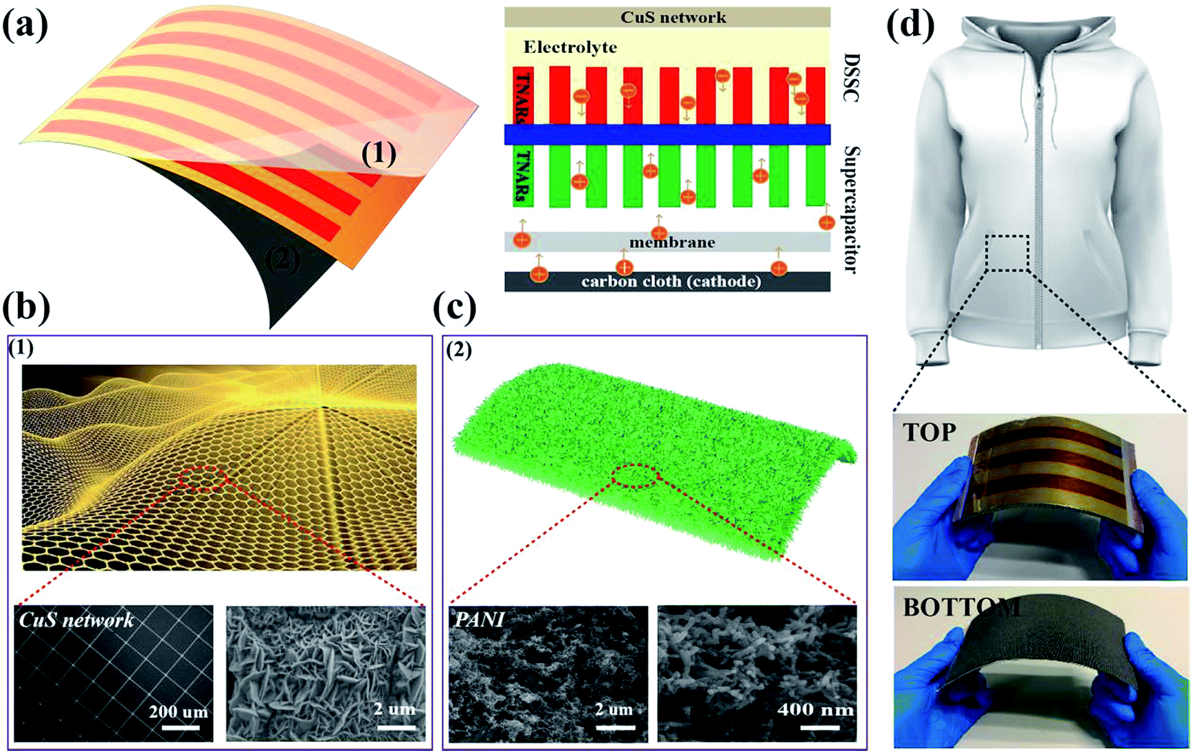 | ||
| Fig. 1 Design and principle of the integrated energy device system. (a) Schematic diagram of the integrated energy device. (b) SEM images of the CuS grid hybrid film obtained from the Cu grid film reaction with saturated sulfur powder solution for the CE of the DSSC. (c) SEM images of the CC–PANI composite electrode, which was prepared by electrochemical deposition and serves as the positive electrode of the SC. (d) Photographs of the top and bottom views of the integrated device. | ||
As shown in Fig. 1a, the upper part is the DSSC, which consists of TNARs as the photo-anode and CuS networks as the CE. The polyaniline films were electrochemically deposited and in situ polymerized36–39 on the Ti slip and carbon cloth to form an asymmetric SC, where a cellulose acetate membrane was used as the separator and PVA/H3PO3 gel as the electrolyte. Fig. 1h presents photographs of the top and bottom views of the integrated device, which demonstrate its flexibility and suitability to stick on the cloth for portable electronics.
Fig. 2 presents the schematic illustration and SEM images of the CuS networks on the ultrathin PET. It is evident that the grids of the networks have a square configuration, where the length of their side (L) is 300 μm and the width of the grid infarction (W) is 10 μm for the Cu networks (Fig. 2a). When flexible Cu mesh was placed in a saturated sulfur solution at 70 °C for 12 h, flower-like CuS was orderly deposited on the mesh on a large scale. The corresponding magnified SEM morphology image is shown in Fig. 2c, which displays that the CuS networks are composed of nanosheets with a thickness of ∼50 nm. Herein, the CuS networks not only serve as conducting films for electron collection from the external circuit but also as superior catalysts for reducing triiodide (I3−) electrolytes. In particular, this commercial film with excellent optoelectronic performances shows good compatibility for fabrication with large-area roll-to-roll property. With the development of encapsulation technology, the use of larger area DSSCs becomes possible beyond that currently used, which depends on the cost of CEs.
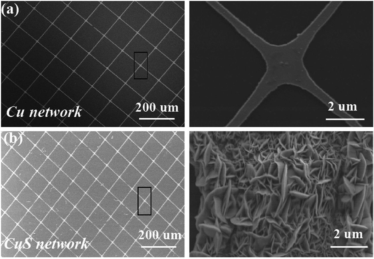 | ||
| Fig. 2 (a) SEM image of the Cu networks and magnified meshes. (b) SEM images of the flower-like CuS generated on the Cu meshes. | ||
Considering practical applications, particularly wearable applications in the future, heat radiation represents a critical index due to the use of liquid electrolytes, which is of importance for comfort and safety during use. Thus, the temperature variation of this CuS network-based CE was traced at different voltage working conditions (Fig. 3a and b). As expected, the transformed CuS network demonstrated a slightly higher temperature compared with that of the pure Cu network film. When the voltage was changed from 1 V to 5 V, the temperature change from 22.8 °C to 24.6 °C was detected for the pure Cu network film by infrared thermal imaging (Fig. 3a). Astoundingly, the slightly higher temperature change from 24.5 °C to 30.6 °C was detected for the CuS network film (Fig. 3b). The average temperatures of 23.5 °C and 26.3 °C were produced for the Cu and CuS network films during long time working at a voltage of 2 V, respectively, demonstrating their suitability for application in a variety of wearable electronic products. As a CE for flexible photo-rechargeable electric energy storage systems, the CuS grids have several outstanding features. First, compared with that of traditional sputtered CuS films, the CuS networks exhibit excellent optoelectronic performances. The average transmittance of CuS networks (∼28 Ω sq−1) is about 90% (Fig. 3b), which is comparable to that of commercial flexible ITO film. Second, the CuS network-based CE exhibits remarkable mechanical flexibility, which was investigated by monitoring the variations in resistance through periodic bending of both the CuS network electrodes and commercial ITO on PETs (as a comparison). To examine its mechanical durability, the electrode was bent to a radius of 0.5 cm, and then released to the initial position 3000 times. As shown in Fig. 3f, negligible changes in the resistance were observed for the CuS grids, indicating the remarkable mechanical flexibility of this network-based TCE. However, the resistance of ITO film exhibits a prominent change after bending, showing significantly undesirable disadvantages with brittleness. Third, the CuS network CE exhibits superior electrochemical catalytic activity, which was evaluated by cyclic voltammetry (CV) in triiodide electrolyte. In the CV curve (Fig. 3e), a slight current density change in the positive and negative potentials after 50 cycles is observed, which indicates that CuS has a better electrochemical stability performance.
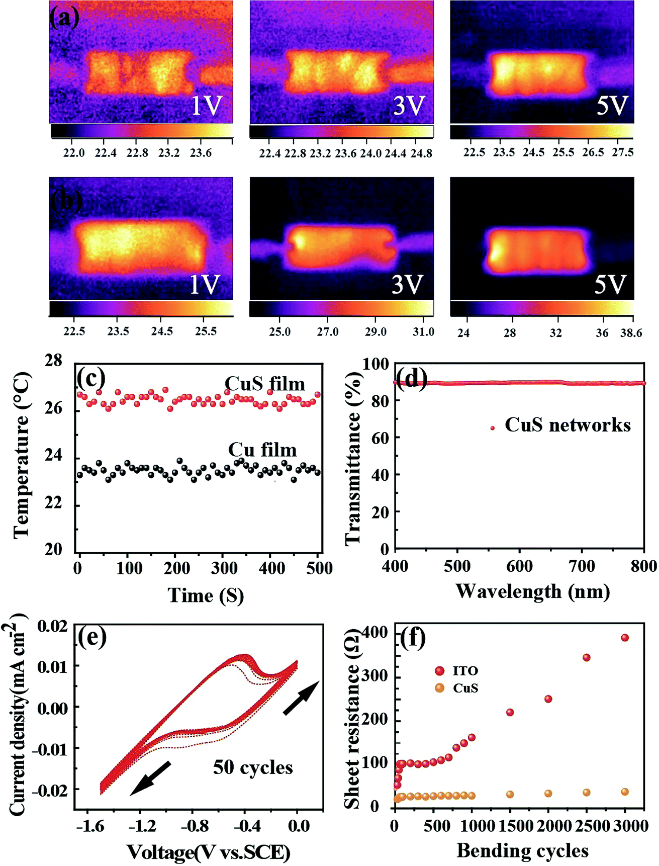 | ||
| Fig. 3 (a) and (b) Infrared camera images of the Cu network film and CuS network film at the potentials of 1 V, 3 V and 5 V, respectively. (c) Temperature variations of the Cu network film and CuS network film at the potential of 2 V. (d) Transmittance spectrum of the as-prepared CuS networks in the wavelength range of 400 nm to 800 nm. (e) Electrochemical catalytic activity of the CuS network film studied by cyclic voltammetry. (f) Mechanical performance test through in different bending cycles of the CuS film and ITO film. | ||
To demonstrate its potential application in flexible electronics, the as-fabricated ultrathin and light DSSCs were used to power a commercial LED in various bending conditions (Fig. 4a). It was found that the tandem DSSCs can not only be rolled as easily as paper but it also can be rolled in different directions. Fig. 4b shows the typical current density–voltage (J–V) characteristics of the photoelectric-conversion part based on the CuS networks and Pt as the CE. The parameters of the DSSC based on the CuS CE have an overwhelming advantage over those of Pt CE. Predictably, the low-cost CuS networks-based CE has a very broad application prospect. In addition to the photovoltaic performance, the bending resistance is another important factor to consider for flexible solar cells. The DSSC was bended with a bending radius of 0.5 cm by mechanical force in different cycles (Fig. 4c). The specific photovoltaic parameters are listed in Table 1. After 100 bending cycles, the open voltage only displays a minute change from 0.76 V to 0.70 V and the photocurrent is reduced from 16.59 mA cm−2 to 15.91 mA cm−2. The fill factor is the most affected, which decreased from 61.05% to 56.32%. These results indicate that the DSSC performance was not affected significantly by mechanical bending. The incident photon to current conversion efficiency (IPCE) spectrum of the device was measured to further investigate its photovoltaic performance; the results are shown in Fig. 4d. The absorption peak located at 400 nm and 550 nm correspond to the dye absorption peak, and the trend of IPCE intensities is consistent with that of the measured photocurrent from the I–V test. Although the single DSSC displays a good performance, its low voltage could not power most small electronic products. Thus, a device with three and five DSSCs in tandem configuration was fabricated, in which the voltage reached 2.6 V and 3.5 V, respectively (Fig. 4e). Furthermore, it was used to drive a commercial red LED successfully (Fig. 4a).
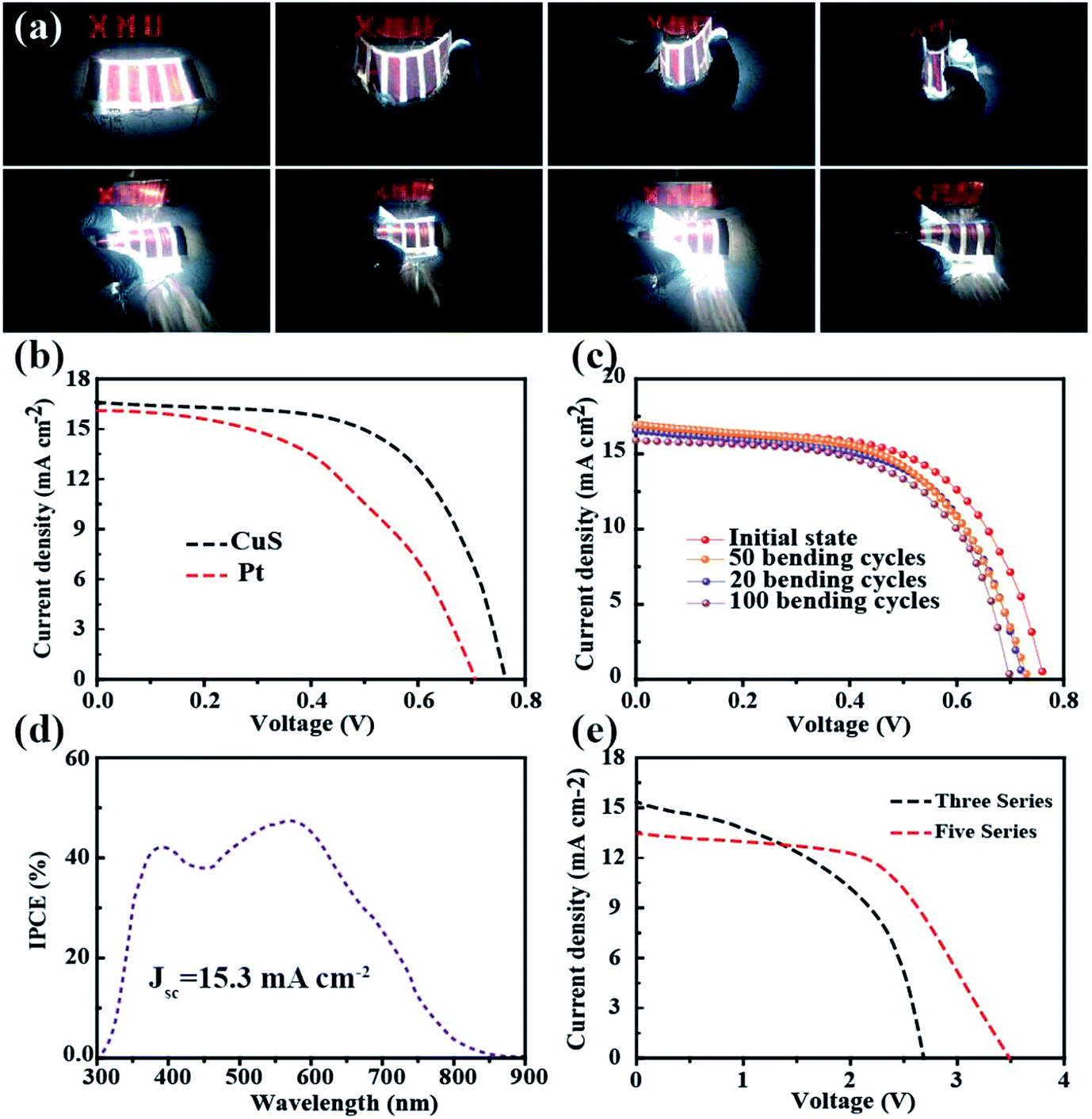 | ||
| Fig. 4 (a) Photographs showing the mechanical flexibility of the ultrathin and light tandem DSSC. (b) J–V curves of the two different DSSCs based on CuS and Pt CEs. (c) J–V curves of the flexible single DSSC with different bending cycles. (d) Incident photo-to-current conversion efficiency (IPCE) curve of the DSSC. (e) J–V curves of several DSSCs in a tandem configuration. | ||
| Jsc [mA cm−2] | Voc [V] | FF [%] | PCE [%] | |
|---|---|---|---|---|
| 0 | 16.59 | 0.76 | 61.05 | 7.73 |
| 20 | 17.89 | 0.73 | 57.65 | 7.55 |
| 50 | 16.99 | 0.72 | 57.23 | 7.01 |
| 100 | 15.91 | 0.70 | 56.32 | 6.21 |
Cyclic voltammetry (CV) and the galvanostatic discharging method were used to characterize the electrochemical properties of the SC as shown in Fig. 5. Fig. 5a shows the CV curves of the asymmetrical SC in the potential window range of 0 V to 0.8 V. The quasi-rectangular shaped curves scanned at 10, 20, 50 and 100 mV S−1 indicate the good electrochemical capacitance of the SC. In order to testify the flexibility of the as fabricated SC, CV tests at normal and bending states were conducted as presented in Fig. 5b. There was only a slight change observed between the two states. The galvanostaic charge–discharge curves were measured at different current densities ranging from 3 mA cm−2 to 10 mA cm−2. As shown in Fig. 5c, the curves exhibit typical asymmetric features with a slightly sloped triangular shape, indicating a good capacitive performance. The as-fabricated device presented an area of capacitance of 375.3 mF cm−2 at a low discharge current density of 3 mA cm−2, which only decreased to 251.4 mF cm−2 when the discharge current density increased to 10 mA cm−2, thus retaining 67% of its initial specific capacitance (Fig. 5d).
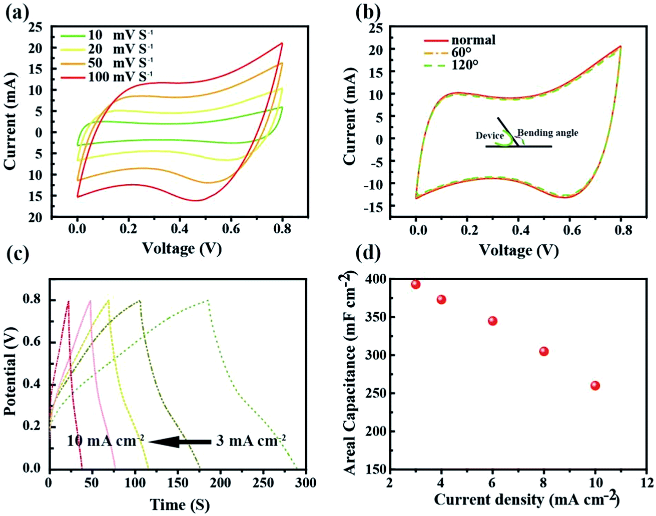 | ||
| Fig. 5 Electrochemical performance of the SC device: (a) CV curves of the SC device at different scan rates. (b) CV curves of the SC device at different bending conditions. (c) GCD curves of the super-capacitor device at different current densities. (d) Area-specific capacitance under different discharge current densities. | ||
To assess the performance parameters of the self-charging energy unit, the DSSC and SC were integrated together (Fig. 1a). When the device was working, the CE of the DSSC and carbon cloth composite electrode of the SC were connected and the voltage of the energy storage part increased to about 0.65 V after 30 s of exposure under AM 1.5G illumination (Fig. 6a). However, the photo-current decreased quickly within a few minutes under light soaking, which could be because the operating voltage was achieved at the Voc, while in fact, the energy output of the DSSC attenuated to a certain degree.40–42 Fig. 6b presents the self-discharge curve of the energy unit after being fully photocharged. The voltage was 80.1% of the initial voltage after self-discharging for 1000 s, which indicates high electrochemical stability. Fig. 6c shows the photo-charging and discharging performance. When the voltage reached 0.64 V, the device was subsequently galvanostatically discharged at a current density of 8 mA cm−2, which could supply electrical energy for 39 s at this current density (Fig. 6c). Next, the photo-rechargeable behavior of the integrated energy unit was tested under bending. As shown in Fig. 6d, the photo-charging and discharging curves remain almost unchanged on bending, which is of great significance for the application of integrated energy devices in portable and wearable electronics. In order to obtain a high photo-charging voltage, the DSSC and SC were connected in series, and ultimately a voltage of 1.9 V was achieved, and the stored energy was utilized.
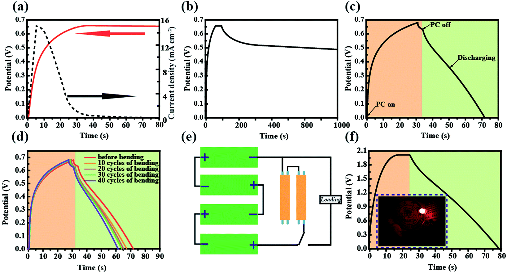 | ||
| Fig. 6 Performance of the integrated device. (a) Voltage–time (red line) and the corresponding photocurrent–time profiles for photo-charging of an integrated system charged to 0.63 V using the DSSC. (b) Self-discharge curve of the SC after being fully photo-charged. (c) Photo-charge galvanostatic discharge curves of the integrated energy device. (c) Voltage–time (V–t) curves of the DSSC-SC integrated device of the photo-charging–discharging process with different bending cycles. (d) Photo-charge/galvanostatic discharge curves of the tandem integrated energy device. (e) Schematic illustration of the tandem integrated energy system for the photo-charge process and discharge process. (f) Photo-charge/galvanostatic discharge curves of the tandem integrated energy device. | ||
The total efficiency of energy conversion and storage (ηtotal) of the energy device can be calculated using the equation: ηtotal = Eoutput/Einput = 0.5Cs × V2 × S0/(Pin × S1 × t), where Eoutput, Cs, V and S0 are the energy output, capacitance, voltage of the energy-storage component and surface area of the SC, respectively. Einput, Pin, S1 and t are the total incident light energy, incident light-energy density, effective area of the energy-conversion component and photocharging time, respectively. According to the curve presented in Fig. 6c, the total efficiency of the integrated device was about 6.5%.
Conclusions
In summary, a flexible, lightweight, integrated energy device has been developed based on a DSSC and supercapacitor. The upper part of the device is composed of DSSC based on TNARs as photo-anode and transparent CuS with high conductivity as CE. The lower region of the integrated device is an SC based on TNARs composited with PANI as the negative electrode and CC–PANI composite materials as the positive electrode, which was used to store electrochemical energy. When the self-powered energy device was irradiated using a standard AM 1.5 (100 mW cm−2) illumination light, the voltage increased to 0.64 V in 30 s, and the discharge time was about 39 s with a current density of 8 mA cm−2. This energy device exhibits a total efficiency of conversion and storage of 6.9%, which is maintained under bending. The present results suggest that the integrated energy device could be woven into wearable, self-powering clothing, which is highly promising in future electronics.Conflicts of interest
There are no conflicts to declare.Acknowledgements
This work was supported by the National Natural Science Foundation of China (No. 515022553, No. U1405226), Beijing Natural Science Foundation (2164076), the Fundamental Research Funds for the Central Universities of China (No. 20720150030), the “111” Project (B16029), Fujian Provincial Bureau of Science & Technology (2014H6022), the 1000 Talents Program from Xiamen University.Notes and references
- R. Liu, L. Ma, S. Huang, J. Mei, E. Li and G. Yuan, J. Phys. Chem. C, 2016, 120, 28480–28488 CAS.
- J. Zhong, Y. Zhang, Q. Zhong, Q. Hu, B. Hu, Z. L. Wang and J. Zhou, ACS Nano, 2014, 8, 6273–6284 CrossRef CAS PubMed.
- K. Cherenack, C. Zysset, T. Kinkeldei, N. Munzenrieder and G. Troster, Adv. Mater., 2010, 22, 5178–5182 CrossRef CAS PubMed.
- Y. Meng, Y. Zhao, C. Hu, H. Cheng, Y. Hu, Z. Zhang, G. Shi and L. Qu, Adv. Mater., 2013, 25, 2326–2331 CrossRef CAS PubMed.
- B. Zhang, H. L. Yu, H. Ni and S. Hu, Nano Energy, 2017, 38, 553–560 CrossRef CAS.
- D. Schmidt, M. D. Hager and U. S. Schubert, Adv. Energy Mater., 2016, 6, 1500369 CrossRef.
- F. T. Li, J. Ran, M. Jaroniec and S. Z. Qiao, Nanoscale, 2015, 7, 17590–17610 RSC.
- J. Zhang, F. Zhao, Z. Zhang, N. Chen and L. Qu, Nanoscale, 2013, 5, 3112–3126 RSC.
- Z. Chai, N. Zhang, P. Sun, Y. Huang, C. Zhao, H. J. Fan, X. Fan and W. Mai, ACS Nano, 2016, 10, 9201–9207 CrossRef CAS PubMed.
- S. Pan, J. Ren, X. Fang and H. Peng, Adv. Energy Mater., 2016, 6, 1501867 CrossRef.
- W. Guo, X. Xue, S. Wang, C. Lin and Z. L. Wang, Nano Lett., 2012, 12, 2520–2523 CrossRef CAS PubMed.
- Z. Zhang, X. Chen, P. Chen, G. Guan, L. Qiu, H. Lin, Z. Yang, W. Bai, Y. Luo and H. Peng, Adv. Mater., 2014, 26, 466–470 CrossRef CAS PubMed.
- Z. Yang, J. Deng, H. Sun, J. Ren, S. Pan and H. Peng, Adv. Mater., 2014, 26, 7038–7042 CrossRef CAS PubMed.
- X. Pu, W. Song, M. Liu, C. Sun, C. Du, C. Jiang, X. Huang, D. Zou, W. Hu and Z. L. Wang, Adv. Energy Mater., 2016, 6, 1601048 CrossRef.
- Z. Wen, M. H. Yeh, H. Guo, J. Wang, Y. Zi, W. Xu, J. Deng, L. Zhu, X. Wang and C. Hu, Sci. Adv., 2016, 2, 1600097 Search PubMed.
- C. Pan, W. Guo, L. Dong, G. Zhu and Z. L. Wang, Adv. Mater., 2012, 24, 3356–3361 CrossRef CAS PubMed.
- H. Zhong, K. Fujii, Y. Nakano and F. Jin, J. Phys. Chem. C, 2015, 119, 55–61 CAS.
- Y.-K. Fuh, P.-C. Chen, Z.-M. Huang and H.-C. Ho, Nano Energy, 2015, 11, 671–677 CrossRef CAS.
- N. Zhang, J. Chen, Y. Huang, W. Guo, J. Yang, J. Du, X. Fan and C. Tao, Adv. Mater., 2016, 28, 263–269 CrossRef CAS PubMed.
- Y. Fang, J. Tong, Q. Zhong, Q. Chen, J. Zhou, Q. Luo, Y. Zhou, Z. Wang and B. Hu, Nano Energy, 2015, 16, 301–309 CrossRef CAS.
- A. Takshi, H. Yaghoubi, T. Tevi and S. Bakhshi, J. Power Sources, 2015, 275, 621–626 CrossRef CAS.
- K. Hagedorn, C. Forgacs, S. Collins and S. Maldonado, J. Phys. Chem. C, 2010, 114, 12010–12017 CAS.
- J. Chen, Y. Huang, N. Zhang, H. Zou, R. Liu, C. Tao, X. Fan and Z. L. Wang, Nat. Energy, 2016, 1, 16138 CrossRef CAS.
- J. Xu, H. Wu, L. Lu, S.-F. Leung, D. Chen, X. Chen, Z. Fan, G. Shen and D. Li, Adv. Funct. Mater., 2014, 24, 1840–1846 CrossRef CAS.
- N. Zhang, J. Chen, Y. Huang, W. Guo, J. Yang, J. Du, X. Fan and C. Tao, Adv. Mater., 2016, 28, 263–269 CrossRef CAS PubMed.
- W. Guo, Z. Xu, F. Zhang, S. Xie, H. Xu and X. Y. Liu, Adv. Funct. Mater., 2016, 26, 8855–8884 CrossRef CAS.
- B. Fang, M. Kim, S. Q. Fan, J. H. Kim, D. P. Wilkinson, J. Ko and J. S. Yu, J. Mater. Chem., 2011, 21, 8742–8748 RSC.
- B. Fang, J. H. Kim, M. S. Kim and J. S. Yu, Acc. Chem. Res., 2013, 46, 1397–1406 CrossRef CAS PubMed.
- B. Fang, S. Q. Fan, J. H. Kim, M. S. Kim, M. Kim, N. K. Chaudhari, J. Ko and J. S. Yu, Langmuir, 2010, 26, 11238–11243 CrossRef CAS PubMed.
- G. Veerappan, K. Bojan and S. W. Rhee, ACS Appl. Mater. Interfaces, 2011, 3, 857–862 CAS.
- J. G. Nam, Y. J. Park, B. S. Kim and J. S. Lee, Scr. Mater., 2010, 62, 148–150 CrossRef CAS.
- T. N. Murakami, S. Ito, Q. Wang, M. K. Nazeeruddin, T. Bessho, I. Cesar, P. Liska, R. Humphry-Baker, P. Comte, P. t. Péchy and M. Grätzel, J. Electrochem. Soc., 2006, 153, 2255 CrossRef.
- J. D. Roy-Mayhew, D. J. Bozym, C. Punckt and I. A. Aksay, ACS Nano, 2010, 4, 6203 CrossRef CAS PubMed.
- C. C. Chen, H. W. Chung, C. H. Chen, H. P. Lu, C. M. Lan, S. F. Chen, L. Luo, C. S. Hung and W. G. Diau, J. Phys. Chem. C, 2008, 112, 19151–19157 CAS.
- M. Ye, X. Xin, C. Lin and Z. Lin, Nano Lett., 2011, 11, 3214–3220 CrossRef CAS PubMed.
- G. F. Yu, X. Yan, M. Yu, M. Y. Jia, W. Pan, X. X. He, W. P. Han, Z. M. Zhang, L. M. Yu and Y. Z. Long, Nanoscale, 2016, 8, 2944–2950 RSC.
- X. Chen, F. Meng, Z. Zhou, X. Tian, L. Shan, S. Zhu, X. Xu, M. Jiang, L. Wang and D. Hui, Nanoscale, 2014, 6, 8140–8148 RSC.
- Y. Liu, Y. Ma, S. Guang, F. Ke and H. Xu, Carbon, 2015, 83, 79–89 CrossRef CAS.
- F. Ke, Y. Liu, H. Xu, Y. Ma, S. Guang, F. Zhang, N. Lin, M. Ye, Y. Lin and X. Liu, Compos. Sci. Technol., 2017, 142, 286–293 CrossRef CAS.
- J. Xu, H. Wu, L. Lu, S. F. Leung, D. Chen, X. Chen, Z. Fan, G. Shen and D. Li, Adv. Funct. Mater., 2014, 24, 1840–1846 CrossRef CAS.
- A. Cohn, W. R. Erwin, K. Share, L. Oakes, A. S. Westover, R. Carter, R. Bardhan and C. L. Pint, Nano Lett., 2015, 15, 2727–2732 CrossRef CAS PubMed.
- R. Liu, J. Wang, T. Sun, M. Wang, C. Wu, H. Zou, T. Song, X. Zhang, S. T. Lee and Z. L. Wang, Nano Lett., 2017, 7, 4240–4247 CrossRef PubMed.
Footnote |
| † Electronic supplementary information (ESI) available. See DOI: 10.1039/c7ra11246g |
| This journal is © The Royal Society of Chemistry 2017 |