
 Open Access Article
 This Open Access Article is licensed under a Creative Commons Attribution-Non Commercial 3.0 Unported Licence
Controllable fabrication of Ag-nanoplate-decorated PAN-nanopillar arrays and their application in surface-enhanced Raman scattering†
Zhongbo Li *ab,
Zhaofang Du*a,
Kexi Sunc,
Xuan Hed and
Bensong Chen*b
*ab,
Zhaofang Du*a,
Kexi Sunc,
Xuan Hed and
Bensong Chen*b
aCollege of Light-Textile Engineering and Art, Anhui Agricultural University, Hefei 230036, China. E-mail: zbli@ahau.edu.cn
bKey Laboratory of Materials Physics, Key Laboratory of Nanomaterials and Nanotechnology, Institute of Solid State Physics, Chinese Academy of Sciences, Hefei, Anhui 230031, China
cCollege of Physics and Electronic Information, Luoyang Normal University, Luoyang 471022, China
dInstitute of Chemical Materials, China Academy of Engineering Physics, Mianyang 621900, China
First published on 17th November 2017
Abstract
We report a facile and low-cost approach for fabrication of large-scale surface-enhanced Raman scattering (SERS) active substrates composed of Ag-nanoplates (Ag-NPs) decorated polyacrylonitrile nanopillar (denoted as Ag-NPs@PAN-nanopillar) arrays, via a consecutive process of molding PAN-nanopillar arrays, sputtering Au-nanoparticles onto the PAN-nanopillar arrays as a conducting layer, and decorating the PAN-nanopillars with Ag-nanoplates. The Ag-nanoplate distribution density on the PAN-nanopillars can be tailored by tuning the concentration of citric acid and the Ag-deposition duration, and high SERS sensitivity can thus be achieved by optimizing the density of Ag-nanoplates. The adjacent Ag-nanoplates induced “hot spots” are densely and uniformly distributed in the three dimensional (3D) space around the PAN-nanopillar arrays, and thus Ag-NPs@PAN-nanopillar arrays generated sensitive and homogenous SERS signals when using rhodamine 6G as a probed molecule. Using the Ag-NPs@PAN-nanopillar arrays as SERS substrates, 10−7 M methyl parathion (organophosphorus insecticide) and 10−6 M PCB-77 (one congener of polychlorinated biphenyls belonging to persistent organic pollutants) are identified. Therefore the SERS-active substrates have potential in SERS-based rapid detection of environmental organic pollutants.
Introduction
Surface-enhanced Raman scattering (SERS) has been developed as one of the most promising ultra-sensitive real time analytical techniques, which has led to major breakthroughs in a number of areas, including biological chemistry, environmental monitoring, and sensor applications.1–8 One of the key issues for SERS-based ultra-trace analysis is rational design and fabrication of SERS substrates with high sensitivity and good signal reproducibility.9,10 It is commonly accepted that SERS enhancement is largely due to the amplification of the local electromagnetic (EM) fields owing to the excitation of surface-plasmon resonance within the so-called “hot spots” located in the nanogaps,11,12 and around the sharp nanoedges13,14 and nanotips of the noble metal nanostructures.15,16 Therefore, a great deal of SERS research has been devoted to the optimization of noble metal (particularly Ag or Au) SERS substrates with high density of uniformly distributed hot spots within diverse nanostructured architectures, such as zero dimensional (0D) single-particles,17 one dimensional (1D) metallic nanoparticle chains,18 two dimensional (2D) self-assembled metallic nanoparticle arrays19 and three dimensional (3D) noble-metal/semiconductor composite micro/nanostructures.20–25 Among them, SERS-active substrates based on the 3D ordered composite micro/nanostructures have attracted ever-increasing attention, as “3D” SERS substrates can achieve high density of 3D electromagnetic “hot spots” and offer large surface areas which are beneficial to the adsorption of target analytes.14,26,27 In addition, the ordered “3D” SERS substrates can ensure better reproducibility and reliability of SERS signals compared to the dispersed noble-metal colloidal nanoparticles.28To date, a large number of “3D” SERS substrates have been achieved via a broad variety of routes. One universal strategy to develop 3D SERS substrates is decorating plasmonic nanostructures (Ag, Au) onto ordered 3D-frameworks such as carbon nanotube arrays,23 bioscaffold arrays,29 glass nanopillar arrays,26 and semiconductors (Si, Ge, ZnO, and TiO2) nanostructure arrays.30–32 Therefore, three types of hot spots can be achieved in the 3D ordered hybrid nanostructure arrays,26,28 i.e., the first one on the top ends of the individual building blocks of 3D-framework, the second one on the sidewalls of individual building blocks of 3D-framework nanoblock, and the third one between the neighboring building blocks of 3D-framework nanoblock. On the other hand, Ag nanoplates have attracted researchers' attention due to their unique sharp edges, which can provide extraordinary localized surface plasmon resonance (LSPR) compared to the traditional Ag nanoparticles (NPs) and can be widely employed as plasmonic nanoscale building blocks for constructing effective SERS substrates.14,33,34 Therefore, if the Ag nanoplates are assembled into the 3D ordered nanoarchitectured frameworks, high density “hot spots” could be achieved in the gaps between the neighboring nanoplates, and thus 3D hierarchical SERS-substrates with high sensitivity and good signal reproducibility could be expected.
Herein, we present a simple and low-cost method for fabricating large-area SERS-active substrates made of vertically aligned PAN-nanopillar arrays decorated with high density Ag nanoplates via a successive process, as shown schematically in Fig. 1. Firstly, large-area highly ordered vertically aligned PAN-nanopillar arrays were facilely prepared. Subsequently, Au nanoparticles are sputtered onto the PAN-nanopillars to service as a conducting layer and also provide nucleation sites for Ag nanostructures to grow. Finally, Ag nanoplates are assembled onto the Au-nanoparticles decorated PAN-nanopillars via simple galvanic cell reaction growth in the presence of citric acid (right part in the Fig. 1). The as-prepared 3D hierarchical Ag-nanoplates decorated PAN nanopillar (denoted as Ag-NPs@PAN-nanopillar) arrays have the following advantages. First, the large-area highly ordered arrays of the PAN-nanopillar arrays can ensure the uniformity and reproducibility of SERS signals. Second, the densely packed Ag nanoplates could be assembled onto the 3D PAN-nanopillar-frameworks via a low cost and simple galvanic-cell-induced growth, and thus highly concentrated electromagnetic fields could be generated near the nanoscale sharp edges of the nanoplates and abundant uniform hot spots could also be achieved in the nano-gaps between the neighboring nanoplates in the hierarchical Ag-NPs@PAN-nanopillar arrays. Furthermore, using the hierarchical Ag-NPs@PAN-nanopillar arrays as sensitive SERS-substrates, R6G, methyl parathion (one of extremely hazardous pesticides35) and PCB-77 (one congener of polychlorinated biphenyls belonging to persistent organic pollutants) with a concentration down to 10−11 M, 10−7 M and 10−6 M can be recognized respectively, showing promising potentials in SERS-based rapid detection of toxic organic pollutants in the environment.
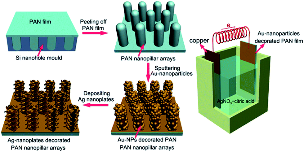 | ||
| Fig. 1 Schematic for the fabrication of Ag-nanoplates-assembled PAN-nanopillar arrays via simple galvanic cell reaction method. | ||
Results and discussion
Fabrication of Ag-NPs@PAN-nanopillar arrays
Fig. 2a and b show the oblique-view scanning electron microscope (SEM) images of the molded uniform PAN-nanopillar arrays on one side, revealing highly ordered hexagonal arrays of nanopillars with diameters of ∼268 nm and center-to-center distances of ∼600 nm (Fig. 2b). The enlarged oblique-view SEM image also reveals the arrays of PAN-nanopillars with heights of ∼550 nm (Fig. 2b). After ion-sputtering Au-nanoparticles onto the surface of the PAN-nanopillars as a conducting layer, dense Ag-nanoplates (Fig. 2c and d) were assembled onto the PAN-nanopillars via a simple galvanic cell reaction growth34 in a mixed electrolyte of AgNO3 and citric acid. After the galvanic cell reaction proceeding for 15 min, the diameter and height of the nanopillars are ∼485 nm (Fig. 2d) and ∼670 nm (Fig. S1a and b of the ESI†), respectively. The enlarged oblique-view and side-view SEM images (Fig. 2d, S1a and b of the ESI†) reveal that cross-linked Ag-nanoplates were uniformly and densely decorated on both the top and the side surfaces of each PAN-nanopillar and high density sub-10 nm gaps are formed between the nearest Ag-nanoplates. Accordingly, the arrays of Ag-nanoplates decorated PAN-nanopillar possess high-density 3D “hot spots” due to strong coupling of such neighboring Ag-nanoplates. Energy dispersive X-ray spectroscopy (EDS) measurement (Fig. S2 of the ESI†) confirms that the nanoplates are composed of Ag. Transmission electron microscopy (TEM) and selected area electron diffraction (SAED) provide further insight into the structure of the Ag-nanoplates. The corresponding close-up TEM view of the products (Fig. 2c) shows the Ag-nanoplates are grafted on the surface of PAN-nanopillars (Fig. 2e), and the lattice-resolved image (Fig. 2f) taken on a single Ag-nanoplate reveals fringes with separated spacing of 2.4 Å, being assigned to the Ag {111} reflection. The inset in Fig. 2f is a typical SAED pattern taken from this nanoplate, showing the polycrystalline electron diffraction feature. The structure of the Ag-NPs@PAN-nanopillar arrays with different deposition durations is also verified by X-ray diffraction (XRD) pattern (Fig. S3 of the ESI†). With prolongation of the Ag deposition duration to 45 min, the corresponding XRD pattern shows four distinguishing diffraction peaks at 38.3, 44.4, 64.4, and 77.6°, corresponding to the (111), (200), (220), and (311) planes of the face-centered cubic (fcc) structure of silver, respectively.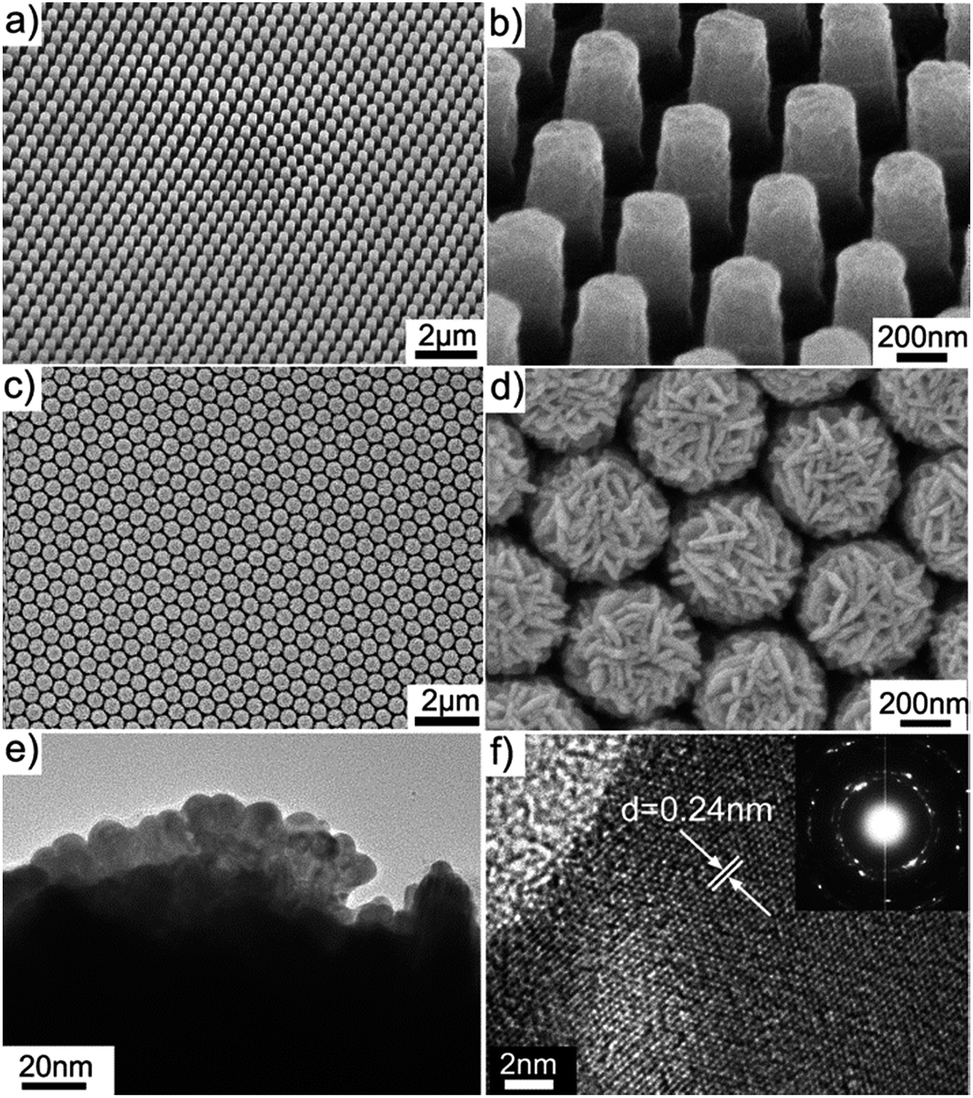 | ||
| Fig. 2 (a and b) SEM images of the as-prepared hexagonal PAN-nanopillar arrays. (c and d) SEM images of Ag-nanoplates-assembled PAN-nanopillars. (e) A close-up TEM view of Ag-nanoplates assembled on one PAN-nanopillar. (f) HRTEM image of a single Ag nanoplate. The inset in (f) is the corresponding selected area electron diffraction (SAED) pattern. | ||
Morphology regulation of Ag-nanostructures wrapped PAN-nanopillar arrays
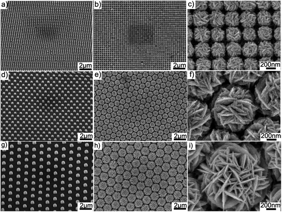 | ||
| Fig. 3 (a) SEM image of tetragonal PAN-nanopillar arrays. (b and c) SEM images of tetragonal Ag-NPs@PAN-nanopillar arrays using the corresponding tetragonal PAN-nanopillar arrays shown in (a). (d) SEM image of the hexagonal PAN-nanopillar arrays (period: 1000 nm). (e and f) SEM images of hexagonal Ag-NPs@PAN-nanopillar arrays using the corresponding hexagonal PAN-nanopillar arrays shown in (d). (g) SEM image of the hexagonal PAN-nanopillar arrays (period: 1500 nm). (h and i) SEM images of hexagonal Ag-NPs@PAN-nanopillar arrays using the corresponding hexagonal PAN-nanopillar arrays shown in (g). | ||
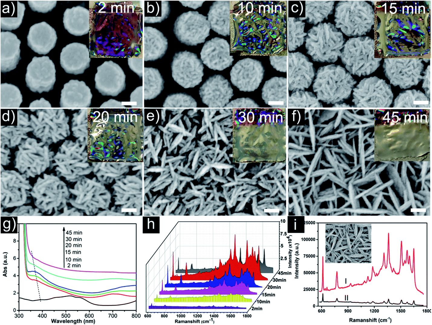 | ||
| Fig. 4 (a–f) SEM images of the Ag-nanoshests-assembled PAN-nanopillar arrays with different Ag-depositing durations. Inset: the photographs of Ag-nanoplates assembled PAN-nanopillar films with different Ag-deposition durations scale bars: 200 nm. (g) The corresponding UV-vis absorption spectra of Ag-NPs@PAN-nanopillar arrays prepared under the different Ag-depositing durations. (h) The SERS spectra of R6G collected on Ag-NPs@PAN-nanopillar arrays with different Ag-depositing durations. (i) The SERS spectra of R6G collected on the Ag-NPs@PAN-nanopillar arrays (curve I) and Ag-nanoplates assembled on the flat PAN film using electrochemical method (curve II); inset is SEM image of the Ag-nanoplates assembled on the flat PAN film using electrochemical method. Scale bars: 500 nm. | ||
Obviously, the Ag-NPs@PAN-nanopillar arrays with 30 min Ag deposition duration exhibit the highest SERS activity, were thus chosen as SERS substrates to investigate the SERS signal sensitivity using R6G as probe molecule. Fig. 5a shows the Raman spectra of R6G with different concentrations (10−8, 10−9, 10−10, and 10−11 M) adsorbed on the Ag-NPs@PAN-nanopillar arrays, displaying high quality SERS signals. As shown in Fig. 5a, the distinct bands can be still easily distinguished in the Raman spectrum even at the low concentration of 10−11 M. The SERS spectra reveal the characteristic peaks of R6G at 612 cm−1 (C–C–C ring in-plane bending mode), 775 cm−1 (C–C–C ring out-of-plane bending mode) and 1361 cm−1 (aromatic C–C stretching vibration mode), respectively.32 The error bar line in Fig. 5b exhibits a correlation coefficient R2 = 0.96 at the range of 10−11M to 10−8 M. The high SERS activity of the hierarchical SERS substrate is also demonstrated by a rough estimation of the enhancement factors (EF) shown in the part S2 of the ESI,† where the 4-aminothiophenol (4-ATP) was used as the probe molecules. The EF can be calculated by the formula EF = (ISERS/NSERS)/(IRef/NRef), where ISERS and IRef represent the relative peak intensities of the SERS spectra and the Raman spectra (non-SERS) respectively; and NSERS and NRef represent the number of probe molecules on the substrates within the laser spot, respectively. The average EF is estimated to be about 9.6 × 10⁶, showing the high SERS activity of the hierarchical SERS substrate.
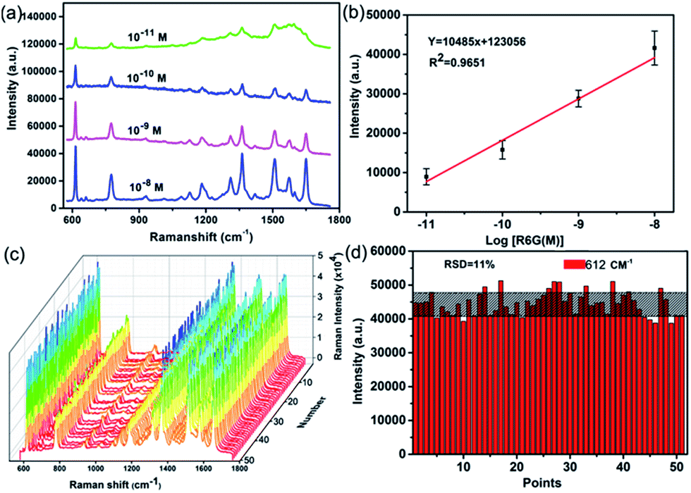 | ||
| Fig. 5 (a) SERS spectra collected on the Ag-NPs@PAN-nanopillar arrays (Fig. 4e) exposed to different concentrations of R6G aqueous solution. (b) The corresponding calibration curve for Raman enhancement (at 612 cm−1) versus log[R6G(M)]. (c) SERS spectra of 10−8 M R6G collected from 50 random spots on the substrate shown in Fig. 4e. (d) The intensity of the peaks at 612 cm−1 from random 50 spots on the substrate. | ||
For SERS-based applications, one of the crucial factors is the reproducibility of Raman signals from SERS substrate. The SERS signal reproducibility was investigated by taking the SERS spectra of R6G from different locations. Fig. 5c shows the SERS spectra of R6G collected at fifty spots on the substrate (Fig. 4e), the average relative standard deviation (RSD) of the intensities of the peaks 612 cm−1 is less than 12% (Fig. 5d), demonstrating a comparable uniformity of the SERS signal across the entire area of the substrate due to the ordered morphological features of the Ag-NPs@PAN-nanopillar arrays. The homogeneity of Ag nanoplate-assembled PAN-nanoarrays is further supported by the SERS images of “hot spots” over the large area. Fig. S8 of the ESI† shows the image for the arrays acquired with a spatial resolution of 1 μM and presented as a color-coded integrated intensity of the characteristic peak of R6G at 612 cm−1. It is obviously seen that the “hot spots” over the Ag nanoplate-assembled PAN-nanopillar arrays are uniform.
To demonstrate potential applications of the as-prepared hierarchical SERS-substrates, the SERS-sensitivity of the Ag-NPs@PAN-nanopillar arrays to methyl parathion (a commonly used organophosphorus pesticide) and PCBs (one class of persistent organic pollutants, defined in the Stockholm Convention) was examined. Fig. 6 shows the SERS spectra of methyl parathion with different concentrations (10−4, 10−5, 10−6, 10−7 M) dispersed on the optimal hierarchical Ag-NPs@PAN-nanopillar arrays. It demonstrates that with a low concentration even down to 10−7 M, the characteristic peaks of 854, 1109, 1251, 1345 and 1592 cm−1 of methyl parathion can still be identified.38 Moreover, PCB-77 (one congener of PCBs) with different concentrations (10−3, 10−4, 10−5 and 10−6M) have been detected, as shown in Fig. S9 of the ESI.† Five fingerprint characteristic peaks at 677, 1030, 1244, 1296 and 1596 cm−1 in the SERS spectra (Fig. S9†) correspond well to the reported results39 and can still be recognized when the concentration of PCB-77 is down to 10−6 M.
 | ||
| Fig. 6 SERS spectra of 10−4, 10−5, 10−6 and 10−7 M methyl parathion probed using the substrate shown in Fig. 4e. | ||
Conclusions
In conclusion, large-scale SERS-active substrates consisting of Ag-nanoplate grafted PAN-nanopillar arrays have been achieved via a low-cost and green synthetic method. The morphology of Ag-NPs@PAN-nanopillar arrays could be regulated by controlling the Si molds with different arrangement patterns, the amount of the citric acid and Ag-deposition duration. The uniform SERS substrates possess both abundant ‘hot spots’ formed between the adjacent Ag-nanoplates, which ensure their excellent SERS-activity and signal repeatability. The Ag-NPs@PAN-nanopillar arrays have been used as SERS substrates for the detection, 10−11 M R6G, 10−7 M methyl parathion, and 10−6 M PCB-77 are identified, showing promising potentials in rapid recognition of chemical pollutants.Experimental section
Materials
Polyacrylonitrile (PAN, Mw 150![[thin space (1/6-em)]](https://www.rsc.org/images/entities/char_2009.gif) 000) was purchased from sigma-Aldrich. Dimethyl formamide (DMF), ethanol (AR), rhodamine 6G (R6G) and methyl parathion were purchased from Shanghai Aladdin Reagent Co. Ltd. (Shanghai, China). PCB-77 was purchased from AccuStandard Inc. The water used in all experiments was ultrapure (18.2 MΩ). All chemicals were used as received without further purification.
000) was purchased from sigma-Aldrich. Dimethyl formamide (DMF), ethanol (AR), rhodamine 6G (R6G) and methyl parathion were purchased from Shanghai Aladdin Reagent Co. Ltd. (Shanghai, China). PCB-77 was purchased from AccuStandard Inc. The water used in all experiments was ultrapure (18.2 MΩ). All chemicals were used as received without further purification.
Preparation of PAN-nanopillar arrays
200–300 μL of as-prepared 8 wt% of PAN DMF solution was casted onto the nanohole array Si mold uniformly. The mold was heated at 80 °C for 15 min to evaporate off the DMF solvent. Then PAN-nanopillar arrays can be achieved and directly transferred onto any substrate.Sputtering Au-nanoparticles onto the PAN-nanopillar arrays
Before sputtering the Au-nanoparticles onto the surfaces of the PAN-nanopillar arrays, the as-prepared PAN-nanopillar arrays were fixed on flat glass wafers. Au-nanoparticles were sputtered on the PAN-nanopillar arrays using a K550X sputter coater with an electric current of 40 mA for 3 min.Preparation of Ag-NPs@PAN-nanopillar arrays via simple galvanic-cell-induced growth method
0.06 g AgNO3 and 0.12 g citric acid were added to 30 mL DI water, followed by stirring until complete dissolution of the solute. The resulting homogeneous solution used as the electrolyte in the experiment was transferred to a galvanic cell. A piece of copper foil (1.5 cm × 1.5 cm) connected to the Au-nanoparticles-sputtered PAN-nanopillar arrays with a conducting wire used as the anode. After the deposition for 15 min at room temperature, the PAN-nanopillar arrays with the products were then taken out, cleaned with DI water several times and dried with high-purity flowing nitrogen.Characterization
The resultant products were characterized by using X-ray diffraction (XRD) (Philips X'pert-PRO), scanning electronic microscope (SEM, sirion 200) with energy-dispersive X-ray spectroscopy (EDS, OXFORD) and Ultraviolet-Visible-Near-Infrared spectrophotometer (Hitachi, U-4100).SERS measurements
SERS measurements for R6G, polychlorinated biphenyls (PCBs) and methyl parathion were performed with the Renishaw inVia microscope equipped with Leica microscope (50 × objective). For the purpose of good molecule adsorption, the Ag-NPs@PAN-nanopillar array substrates were immersed in 1 mL R6G aqueous solution with different concentrations (from 10−7 to 10−11 M) for 3 hours, taken out and then dried with high-purity flowing nitrogen. For the purpose of good molecule adsorption, the substrates were immersed in methyl parathion solution with different concentrations and PCB-77 n-hexane solutions with different concentrations for 5 hours, taken out and then dried with high-purity flowing nitrogen. SERS measurements were carried out under a confocal microprobe Raman system (Renishaw, inVia) with an excitation wavelength of 532 nm. The exposure times for R6G, methyl parathion and PCB-77 were 5 s, 10 s and 30 s.Raman mappings of “hot spots” over Ag-NPs@PAN-nanopillar arrays were performed on Raman imaging system (Renishaw, inVia). R6G (10−8 M) was used as molecular probe. A 532 nm laser was scanned over the substrates and Raman spectra were collected as a function of position. Renishaw WiRE 3.2 software was used to data acquisition and control.
Conflicts of interest
There are no conflicts to declare.Acknowledgements
This work was supported by National Key Basic Research Program of China (Grant No. 2013CB934304), NSFC (51501183), Talent Project of Anhui Agriculture University (yj2017-12).Notes and references
- D. Graham and R. Goodacre, Chem. Soc. Rev., 2008, 37, 883–884 RSC.
- R. A. Tripp, R. A. Dluhy and Y. Zhao, Nano Today, 2008, 3, 31–37 CrossRef CAS.
- J. F. Li, Y. F. Huang, Y. Ding, Z. L. Yang, S. B. Li, X. S. Zhou, F. R. Fan, W. Zhang, Z. Y. Zhou, Y. WuDe, B. Ren, Z. L. Wang and Z. Q. Tian, Nature, 2010, 464, 392–395 CrossRef CAS PubMed.
- K. V. Kong, Z. Lam, W. D. Goh, W. K. Leong and M. Olivo, Angew. Chem., 2012, 124, 9934–9937 CrossRef.
- K. Saha, S. S. Agasti, C. Kim, X. Li and V. M. Rotello, Chem. Rev., 2012, 112, 2739–2779 CrossRef CAS PubMed.
- J. Ando, M. Asanuma, K. Dodo, H. Yamakoshi, S. Kawata, K. Fujita and M. Sodeoka, J. Am. Chem. Soc., 2016, 138, 13901–13910 CrossRef CAS PubMed.
- L. Yang, P. Li and J. Liu, RSC Adv., 2014, 4, 49635–49646 RSC.
- K. Zhao, C. Wu, Z. Deng, Y. Guo and B. Peng, RSC Adv., 2015, 5, 52726–52736 RSC.
- M. J. Banholzer, J. E. Millstone, L. Qin and C. A. Mirkin, Chem. Soc. Rev., 2008, 37, 885–897 RSC.
- B. Shang, Y. Wang, P. Yang, B. Peng and Z. Deng, Sens. Actuators, B, 2018, 255, 995–1005 CrossRef CAS.
- H. Im, K. C. Bantz, S. H. Lee, T. W. Johnson, C. L. Haynes and S.-H. Oh, Adv. Mater., 2013, 25, 2678–2685 CrossRef CAS PubMed.
- Y. Li, M. L. Simeral and D. Natelson, J. Phys. Chem. C, 2016, 120, 22558–22564 CAS.
- Y. Lu, G. L. Liu, J. Kim, Y. X. Mejia and L. P. Lee, Nano Lett., 2005, 5, 119–124 CrossRef CAS PubMed.
- C. Zhu, G. Meng, Q. Huang, X. Wang, Y. Qian, X. Hu, H. Tang and N. Wu, Nano Res., 2015, 8, 957–966 CrossRef CAS.
- A. Kim, F. S. Ou, D. A. A. Ohlberg, M. Hu, R. S. Williams and Z. Li, J. Am. Chem. Soc., 2011, 133, 8234–8239 CrossRef CAS PubMed.
- C. Zhu, G. Meng, P. Zheng, Q. Huang, Z. Li, X. Hu, X. Wang, Z. Huang, F. Li and N. Wu, Adv. Mater., 2016, 28, 4871–4876 CrossRef CAS PubMed.
- Y. Feng, Y. Wang, H. Wang, T. Chen, Y. Y. Tay, L. Yao, Q. Yan, S. Li and H. Chen, Small, 2012, 8, 246–251 CrossRef CAS PubMed.
- J.-C. Valmalette, Z. Tan, H. Abe and S. Ohara, Sci. Rep., 2014, 4, 5238 CrossRef CAS PubMed.
- H. Wang, C. S. Levin and N. J. Halas, J. Am. Chem. Soc., 2005, 127, 14992–14993 CrossRef CAS PubMed.
- X. He, C. Yue, Y. Zang, J. Yin, S. Sun, J. Li and J. Kang, J. Mater. Chem. A, 2013, 1, 15010–15015 CAS.
- S. Y. Lee, S.-H. Kim, M. P. Kim, H. C. Jeon, H. Kang, H. J. Kim, B. J. Kim and S.-M. Yang, Chem. Mater., 2013, 25, 2421–2426 CrossRef CAS.
- R. Kattumenu, C. H. Lee, L. Tian, M. E. McConney and S. Singamaneni, J. Mater. Chem., 2011, 21, 15218–15223 RSC.
- S. Lee, M. G. Hahm, R. Vajtai, D. P. Hashim, T. Thurakitseree, A. C. Chipara, P. M. Ajayan and J. H. Hafner, Adv. Mater., 2012, 24, 5261–5266 CrossRef CAS PubMed.
- F. Jiang, S. Wang, L. Li, H. Jin, W. Zhang, J. Lin, T. Tang and J. Wang, Green Chem., 2011, 13, 2831–2836 RSC.
- S. Jones, S. S. Sinha, A. Pramanik and P. C. Ray, Nanoscale, 2016, 8, 18301–18308 RSC.
- Y.-J. Oh and K.-H. Jeong, Adv. Mater., 2012, 24, 2234–2237 CrossRef CAS PubMed.
- K. Zhao, J. Zhao, C. Wu, S. Zhang, Z. Deng, X. Hu, M. Chen and B. Peng, RSC Adv., 2015, 5, 69543–69554 RSC.
- Z. Li, G. Meng, Q. Huang, X. Hu, X. He, H. Tang, Z. Wang and F. Li, Small, 2015, 11, 5452–5459 CrossRef CAS PubMed.
- F. Shao, Z. Lu, C. Liu, H. Han, K. Chen, W. Li, Q. He, H. Peng and J. Chen, ACS Appl. Mater. Interfaces, 2014, 6, 6281–6289 CAS.
- M. S. Schmidt, J. Hübner and A. Boisen, Adv. Mater., 2012, 24, OP11–OP18 CAS.
- X. Li, G. Chen, L. Yang, Z. Jin and J. Liu, Adv. Funct. Mater., 2010, 20, 2815–2824 CrossRef CAS.
- J. Liu, G. Meng, Z. Li, Z. Huang and X. Li, Nanoscale, 2015, 7, 18218–18224 RSC.
- I. Pastoriza-Santos and L. M. Liz-Marzan, J. Mater. Chem., 2008, 18, 1724–1737 RSC.
- Z. Li, G. Meng, Q. Huang, C. Zhu, Z. Zhang and X. Li, Chem.–Eur. J., 2012, 18, 14948–14953 CrossRef CAS PubMed.
- G. K. Isbister, K. Mills, L. E. Friberg, M. Hodge, E. O'Connor, R. Patel, M. Abeyewardene and M. Eddleston, Clin. Toxicol., 2007, 45, 956–960 CrossRef CAS PubMed.
- H. Tang, G. Meng, Z. Li, C. Zhu, Z. Huang, Z. Wang and F. Li, Nano Res., 2015, 8, 2261–2270 CrossRef CAS.
- X. C. Jiang, C. Y. Chen, W. M. Chen and A. B. Yu, Langmuir, 2010, 26, 4400–4408 CrossRef CAS PubMed.
- D. Lee, S. Lee, G. H. Seong, J. Choo, E. K. Lee, D.-G. Gweon and S. Lee, Appl. Spectrosc., 2006, 60, 373–377 CrossRef CAS PubMed.
- Q. Zhou, Y. Yang, J. Ni, Z. Li and Z. Zhang, Nano Res., 2010, 3, 423–428 CrossRef CAS.
Footnote |
| † Electronic supplementary information (ESI) available. See DOI: 10.1039/c7ra11102a |
| This journal is © The Royal Society of Chemistry 2017 |