
 Open Access Article
 This Open Access Article is licensed under a
 Creative Commons Attribution 3.0 Unported Licence
Structural and photocatalytic properties of Pd-deposited semiconductors with different morphology†
Aramice. Y. S. Malkhasian* and
Katabathini Narasimharao *
*
Department of Chemistry, Faculty of Science, King Abdulaziz University, P. O. Box 80200, Jeddah 21589, Saudi Arabia. E-mail: nkatabathini@kau.edu.sa; aramice.malkhasian@gmail.com; Fax: +966-26952000; Tel: +966-538638994
First published on 8th December 2017
Abstract
In this work, we studied the effect of Pd deposition (0.3 wt%) on the structural and photocatalytic properties of TiO2 anatase with different morphologies (nanoparticles, nanotubes and nanofibers). The Pd-deposited semiconductor samples were synthesized by a simple deposition–precipitation method and used as catalysts for photocatalytic degradation of p-nitrophenol under visible light illumination. Pd-deposited TiO2 nanofibers showed higher photocatalytic activity than Pd-deposited TiO2 nanoparticles or nanotubes. Pd-deposited (0.3 wt%) CeO2 and WO3 nanofibers were also synthesized to investigate whether the advantages of nanofiber morphology extend to other semiconductors, with lower and higher band gap energies. The performance of Pd-deposited CeO2 nanofibers was superior to that of all other Pd-deposited samples. The samples were characterized by elemental analysis, XRD, SEM, TEM, DR UV-vis, N2 physisorption and XPS to investigate the role of structural properties on photocatalytic performance. The XRD data indicated that the crystal structures of TiO2, WO3 and CeO2 were not modified after Pd deposition and TEM indicated that the Pd was well dispersed on the semiconductor surfaces, with particle sizes <20 nm. Pd deposition changed the morphology of the CeO2 nanofibers to a unique ‘mat-like’ structure, with small (4 nm) Pd nanoparticles. This latter sample had the highest photocatalytic activity, which was attributed largely to high photocurrent density. Conditions for photocatalysis were investigated and Pd-deposited CeO2 nanofibres were shown to be reusable for at least five cycles, without significant loss of photocatalytic activity. Our study suggests that Pd-deposited CeO2 nanofibres could be used industrially to degrade p-nitrophenol.
1. Introduction
Photocatalysis has emerged as a viable alternative for many applications, including utilization of solar energy,1 CO2 reduction2 and removal of organic contaminants.3 The development of suitable photocatalytic processes for the purification of contaminated waters and air is of particular interest since photocatalysts can completely degrade organic contaminants into CO2 and H2O. p-Nitrophenol (p-NP) is commonly used as an intermediate in the manufacture of medicines, pesticides, dyes and fine chemicals4 and is often discharged in waste water. This creates environmental problems since p-NP is toxic and carcinogenic and has very low biodegradability. It is, therefore, very important to remove p-NP from effluents before they are discharged into the ecosystem.5Since its discovery by Fujishima and Honda,1 TiO2 has attracted considerable interest as a wide band gap semiconductor. TiO2 has frequently been used as a heterogeneous photocatalyst because it is inexpensive and has low toxicity. The main drawbacks in effective commercial application of TiO2 are its large band gap energy (3.2–3.4 eV), which precludes the use of sunlight, and agglomeration of particles after use, which has a negative effect on photocatalytic activity.6 A number of strategies have been adopted to shift the TiO2 absorption spectrum towards the visible light region to enable its use as an effective photocatalyst in sunlight. The incorporation of precious and non-precious metals7 into the TiO2 lattice is one way to tune the band gap energy.8 The precious metals have been suggested to enhance photocatalytic activity by (i) enhancing the adsorption of organic molecules onto the photocatalytic surface; (ii) increasing electron excitation and electron–hole separation through surface plasmon resonance of precious metal nanoparticles on the semiconductor and (iii) acting as electron traps to hinder electron/hole recombination.9 The presence of Pd on the surface of ZnO has been shown to have a large effect on photocatalytic activity, in both the UV and visible regions of the spectrum. Liqiang et al.10 attributed the increased photocatalytic efficiency in the presence of Pd to increased amounts of adsorbed oxygen on the surface. TiO2 nanotubes incorporating Pd nanoparticles have been used for the photocatalytic decomposition of dyes under sunlight.11 Pd/TiO2 nanotubes completely degraded the dye more quickly than TiO2 nanotubes (150 min versus 250 min). Incorporation of Pd into TiO2 also improved hydrogen production compared with pure TiO2.12 Au–TiO2 and Pt–TiO2 catalysts have been reported to provide 90–100% degradation of p-NP in 300 min using visible light irradiation.13 Degradation of p-NP in visible light has also been reported using Fe3O4–N-doped TiO2 with continuous air bubbling14 and using TiO2–graphene–Pd nanowires.15
The different photocatalytic performances observed for different samples are likely influenced by factors such as composition, crystallinity, surface area and morphology of the active particles.16 Different materials investigated include macro–mesoporous TiO2,17 WO3 microspheres18 and a Pd–CeO2 nanocomposite, which had enhanced photocatalytic activity under visible light.19 Semiconductor materials with different shapes (spheres, cubes, tubes, wires, rods, sheets and flakes), sizes and dimensions can be synthesized by varying the method of preparation and calcination temperature.20 Suzuki et al.21 suggested that there are still many possibilities for improving the photocatalytic activity of semiconductors, especially by altering their morphology. Campelo et al.22 showed that there are some benefits in using nanosized Pd-containing photocatalysts since the Pd nanostructures have enhanced light-harvesting ability. Pd nanostructures were reported to show better photocatalytic activity compared with Ag and Au nanostructured catalysts.
In the present work, we have studied the effect of Pd deposition (0.3 wt%) on the structural and photocatalytic properties of nanostructured semiconductors with different morphologies (particles, tubes and fibers). The Pd-deposited samples were synthesized by a simple deposition–precipitation method and the synthesized materials were used as catalysts for photocatalytic degradation of p-NP under visible light. Pd-deposited TiO2 nanofibers (Pd–Ti-NF) showed higher photocatalytic activity than Pd-deposited TiO2 nanoparticles (Pd–Ti-NP) or nanotubes (Pd–Ti-NT). Because of the superiority of the nanofiber morphology, we also wished to synthesize Pd-deposited WO3 and CeO2 nanofibers to investigate whether the effect of morphology extended to other semiconductors with lower and higher band gap energies. The synthesized samples were characterized structurally and morphologically using different techniques and their efficiency as catalysts for photocatalytic degradation of p-NP under visible light at room temperature was compared.
2. Experimental
2.1 Materials
All the commercial reagents were analytical grade and used as received without any purification. Titanium isopropoxide [C12H28O4Ti], palladium chloride [PdCl2], ethyl alcohol [C2H5OH], hydrochloric acid [HCl], sodium carbonate [Na2CO3], sodium hydroxide [NaOH] solution, p-nitrophenol [C6H5NO3] and tetrapropyl ammonium hydroxide [(CH3CH2CH2)4N(OH)] solution were purchased from Aldrich, U.K.2.2 Preparation of semiconductors with different morphology
2.3 Characterization of synthesized samples
The powder XRD patterns are collected by using Philips PW1700 diffractometer at room temperature. The XRD patterns were obtained using Cu Kα radiation and graphite monochromator with automatic divergent slit. The collected patterns were matched with standard JCPDS files. The crystallite size was calculated from (101) reflection of anatase phase using the Scherrer formula.
D = Bλ/β1/2![[thin space (1/6-em)]](https://www.rsc.org/images/entities/char_2009.gif) cosθ cosθ
| (1) |
A Philips CM200FEG microscope operated at 200 kV, equipped with a field emission gun was used for TEM analysis. The coefficient of spherical aberration was Cs = 1.35 mm. High-resolution images with a pixel size of 0.044 nm were taken with a CCD camera. Field emission scanning electron microscopy (FESEM) images of the samples were collected using on a FEI Nova NANOSEM 230 spectrophotometer. N2-physisorption measurements were carried at −196 °C as per the recommendations of the IUPAC using ASAP 2010 Micromeritics Instrument. Specific surface area (SBET) values were calculated by applying the BET equation. The average pore width was calculated by the BJH method as well as the average pore width method (employing the relation 4 Vp/SBET, where Vp is the specific pore volume).
DR UV-vis spectra for synthesized samples were collected using U-4100, Hitachi spectrophotometer equipped with an integrating sphere in the wavelength range 200–800 nm to measure the reflectance spectra of each sample. Band gap of all the synthesized samples was determined using Kubelka–Munk method. The Kubelka–Munk transformation (K) was estimated using the equation;
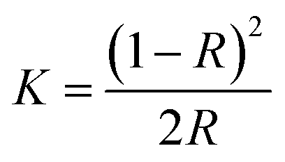 | (2) |
The bulk composition of synthesized samples was determined using inductively coupled plasma-atomic emission spectroscopy (ICP-AES; IRIS Advantage). The XPS measurements were carried out using ESCA Lab 220i-XL spectrometer using Al Kα X-rays. Peak shift due to charge compensation was corrected using the binding energy of C 1s peak. The data was acquired using pass energy of 100 eV, dwell time 200 ms with step size of 0.1 eV and 30 scans.
2.4 Photocatalytic degradation of p-nitrophenol (p-NP)
The photocatalytic degradation of p-NP was performed in a Pyrex glass reactor using synthesized catalysts under the visible light illumination for various time intervals. The p-NP (100 ppm) solution was prepared in 100 mL deionized water and 0.4 g L−1 of catalyst was added to the solution. The resulting suspension was equilibrated by stirring for 45 min to stabilize the adsorption of p-NP over the surface of the catalyst in the dark. The photocatalytic degradation of p-NP was monitored by measuring the absorbance of p-NP at regular time interval using a SmartSpec 3000, Bio-Rad Laboratories Inc., USA. The degradation percentage was calculated using the expression| η = (1 − C/C0) × 100 | (3) |
The stability of the photocatalysts was studied by measuring reusability of the samples. After the first cycle of the activity measurement, the catalyst was filtered from the reactor and the aliquots by centrifugation. The obtained catalyst was thoroughly washed with distilled water and acetone. The catalyst was dried at 80 °C for 2 hours and then reused for the next cycle of the photocatalysis measurements. Similarly, the experiment was repeated for five cycles to study the stability of the catalyst for repetitive use.
3. Results and discussion
3.1 Powder X-ray diffraction
Powder X-ray diffraction (XRD) measurements were used to investigate the phase structure and particle size of the catalysts. The XRD patterns (Fig. 1) showed that the Pd-deposited TiO2 nanostructures were composed of anatase, as a single phase [JCPDS no. 21-1227]. The diffraction peaks at 2θ = 25.3°, 37.8°, 48.0°, 55.0° and 62.7° could be assigned to (101), (004), (200), (211) and (204) planes, respectively, of anatase. The patterns obtained also confirmed the absence of rutile and brookite phases. The XRD pattern of Pd–Ti-NP showed sharp diffraction peaks whereas the Pd–Ti-NF sample showed broad diffraction peaks. This indicates that Pd–Ti-NF has a smaller crystallite size than Pd–Ti-NT or Pd–Ti-NP. The Pd–Ce-NF sample showed reflections attributable to (111), (200), (220) and (311) planes, corresponding to the cubic fluorite structure of CeO2 [JCPDS no. 75-0076], while the Pd–W-NF sample showed diffraction peaks corresponding to the monoclinic WO3 phase. Reflections due to Pd metal or PdO were not detected by XRD in the 2θ region from 20° to 80° for any of the Pd-deposited semiconductor samples. It is possible that the deposited Pd is highly dispersed on the surface of the semiconductors or the size of the crystallites could be smaller than the detection range of the XRD technique.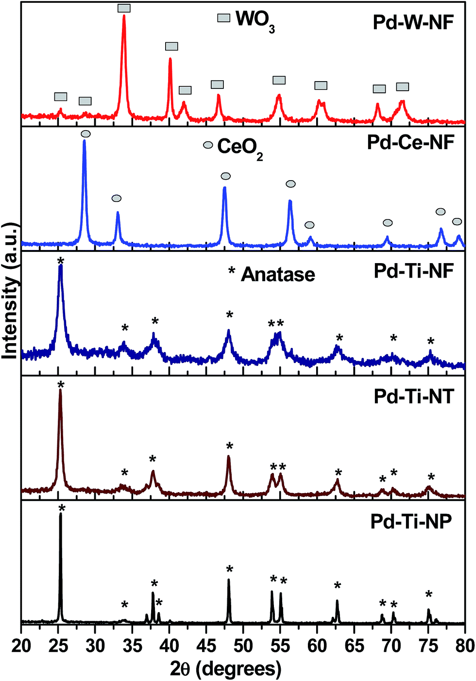 | ||
| Fig. 1 Powder XRD patterns of Pd deposited semiconductor samples. | ||
The average crystallite sizes of the semiconductor phases (TiO2, CeO2 and WO3) were calculated using the Scherrer equation. The crystallite sizes of TiO2 nanoparticles, TiO2 nanotubes and TiO2 nanofibers were 180 nm, 83 nm and 25 nm, respectively (Table 1). The crystallite size of none of the nanostructures was changed after depositing Pd, indicating that the Pd was deposited onto the surface of the semiconductors and not incorporated into the lattices.
3.2 Morphology studies
Scanning electron microscopy (SEM) and transmission electron microscopy (TEM) were used to investigate the size and morphology of the semiconductors and Pd-deposited semiconductors in order to determine the importance of these factors for photocatalytic ability. TEM images of the Pd-deposited semiconductors after calcination at 400 °C for 4 h are shown in Fig. 2 (insets show SEM images before deposition). The fibers in TiO2-NF were ∼3 μm in length and ∼9 nm in diameter. The length of the fibers in Pd–Ti-NF was reduced from μm to nm. It is clear that Pd deposition and thermal treatment led to the formation of Pd nanoparticles and that some of the particles were coordinated with the surface of the nanofibers. The SEM image of TiO2-NP particles showed irregularly shaped, spherical particles and the TEM image of Pd–Ti-NP showed very similar morphology, with dark shaded TiO2-NP particles attributable mostly to the presence of Pd nanoparticles. This sample consisted of agglomerated TiO2 particles with diameters in the range 100–180 nm. The TiO2-NT consisted of anatase nanotubes with an average size of ∼50 nm. The Pd–Ti-NT sample also showed tube-like morphology, but with shorter NTs.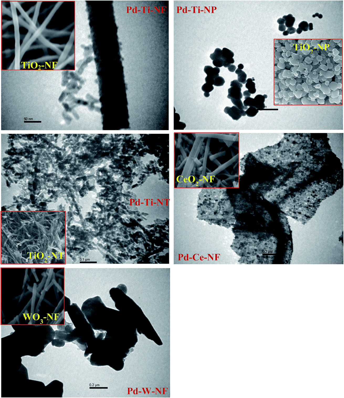 | ||
| Fig. 2 TEM images of Pd deposited semiconductor samples (inset: SEM image before deposition). | ||
The morphologies of Pd–Ce-NF and Pd–W-NF were remarkably different from those of bulk samples of CeO2-NF and WO3-NF. The TEM image of Pd–Ce-NF showed a unique ‘mat-like’ structure, with the deposited Pd visible as small black dots on the surface of the CeO2. Zhang et al.26 also observed that CeO2 adopts a readily distinguishable ‘mat-like’ morphology, and it appears that this unique structure inhibits the aggregation of metal nanoparticles. The TEM image of Pd–W-NF showed that the WO3 had formed nanorods (length 50–150 nm), with the deposited Pd visible as small particles on the surface of the nanorods. These results clearly indicate that the deposition of Pd has a significant effect on the morphology of CeO2 and WO3 nanofibers.
All of the Pd-deposited semiconductor samples showed very small Pd nanoparticles, which were dispersed on the surface of semiconductor. Pd–Ti-NF and Pd–Ce-NF, particularly, had small uniform Pd nanoparticles, with average sizes in the range 3–5 nm. In contrast, Pd–Ti-NT, Pd–Ti-NP and Pd–W-NF showed slightly larger Pd particles, with average sizes of 8–15 nm. No agglomerated particles were observed, demonstrating that the deposition–precipitation method used in this study hindered aggregation of the Pd nanoparticles. Particle sizes measured by TEM analysis and crystallite sizes of the Pd-deposited semiconductor samples calculated using the Scherrer equation are compared in Table 1. Particle sizes of the semiconductor samples determined from TEM are smaller than those determined from XRD measurements, probably because of slight changes in morphology and agglomeration of the semiconductor samples.
The particles sizes of Pd species dispersed on Pd–Ti-NP and Pd–W-NF were larger than those of Pd particles dispersed on Pd–Ce-NF and Pd–Ti-NF, probably because the interaction of Pd with nanofibers is different in semiconductors with different morphologies. It has been reported that small Pd nanoparticles can dissociate into Pd atoms at high temperatures (800 °C),27 but since the Pd-deposited samples synthesized in the present study were heated to only 500 °C, dissociation of Pd would not have occurred.
3.3 Diffuse reflectance UV-vis spectroscopy
Diffuse reflectance (DR) UV-vis spectra of bare and Pd-deposited semiconductor samples showed marked differences (Fig. 3). The bare TiO2 nanostructured samples showed a UV-vis absorption peak centered at ∼250 nm, which can be attributed to electron transfer from the valence band to the conduction band of TiO2.28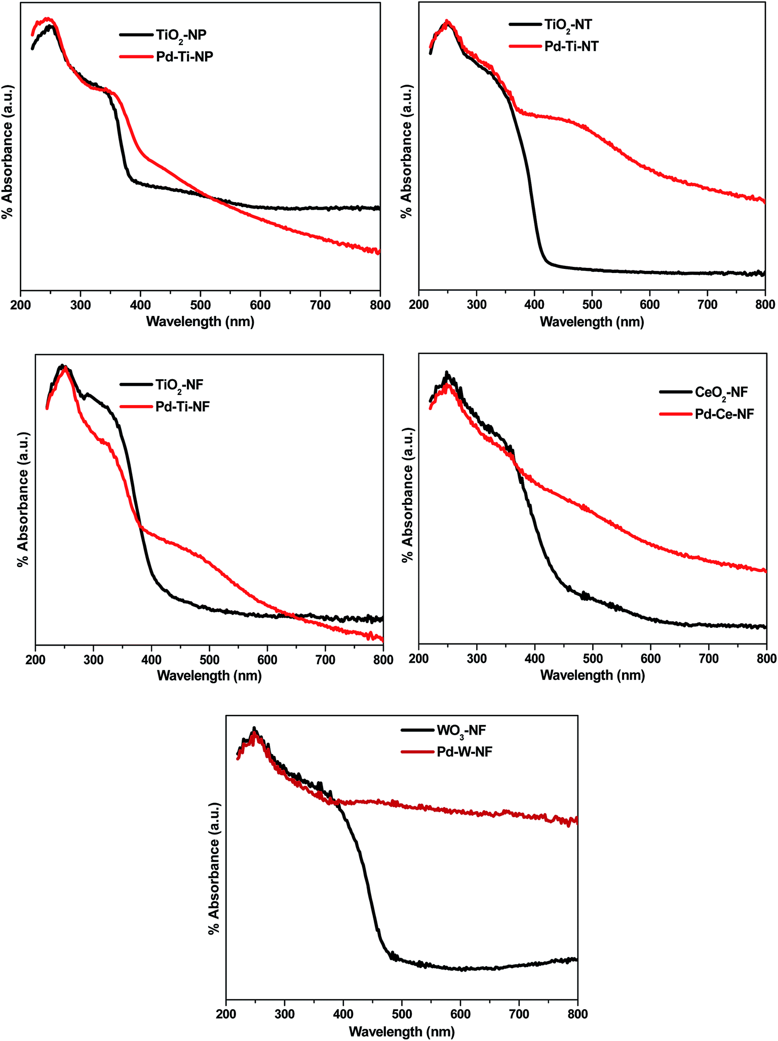 | ||
| Fig. 3 DR UV-vis spectra of bare and Pd deposited semiconductor samples. | ||
The DR UV-vis spectra showed that Pd-deposited semiconductor samples absorb more visible light than bare semiconductor samples. The Pd-deposited samples also showed a slight red shift in the absorption edge, indicating that Pd deposition is responsible for the absorption of light in the visible region. Additionally, a wide absorption peak, centered at 480 nm, appeared in all Pd-deposited semiconductor samples, indicating the presence of plasmonic Pd nanoparticles on the semiconductor surface.29 This demonstrates the existence of surface plasmon resonance (SPR) in the Pd-deposited semiconductor samples.
Band gap energy values for all the synthesized samples were calculated by plotting the Kubelka-Munk function (K) against energy (eV). The calculated values of band gap energy for Pd–Ti-NF, Pd–Ti-NT and Pd–Ti-NP were 2.96 eV, 2.98 eV and 3.01 eV, respectively, which are all lower than that of bare anatase (3.40 eV). The band gap energy values for Pd–Ce-NF and Pd–W-NF samples were calculated as 2.92 eV and 2.88 eV, respectively, which are likewise smaller than values for bare CeO2 and WO3 samples. It can be concluded, therefore, that deposition of Pd had an effect on the optical properties of the different semiconductor samples.
3.4 N2 physisorption
N2 adsorption–desorption isotherms for bare and Pd-deposited semiconductor samples are shown in Fig. 4. The samples of bare TiO2-NP and Pd–Ti-NP clearly showed type-IV isotherms with H2-type hysteresis loops as per the IUPAC classification, demonstrating that both samples contain mesoporous pores. A relatively smaller hysteresis loop was observed after Pd deposition on TiO2-NP. Samples of bare TiO2-NT and Pd–Ti-NT also showed type-IV isotherms.30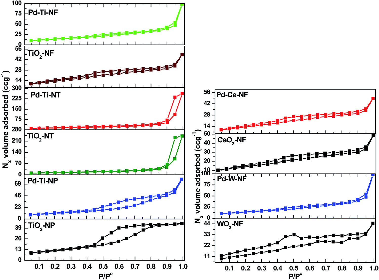 | ||
| Fig. 4 N2 adsorption–desorption isotherms of the bare and Pd deposited semiconductor samples. | ||
Nanotube samples showed H1-type hysteresis loops, indicating the presence of uniform cylindrical pore structures in these samples. The isotherms of bare and Pd-deposited TiO2-NF, CeO2-NF and WO3-NF were identified as type-III. Nanofibrous samples (specifically WO3-NF) thus showed weak adsorption of N2 molecules, indicating that these samples possess very few micropores or mesopores. An increase in the volume of adsorbed N2 was, however, observed at high pressures (0.89–0.99), revealing the presence of macropores in the hollow structures of the nanofibers. The specific surface area (SBET), average pore diameter and pore volume were obtained from the N2 physisorption measurements (Table 2). The SBET was calculated using the BET equation. SBET values for bare TiO2-NP, TiO2-NT and TiO2-NF were 70 m2 g−1, 53 m2 g−1 and 45 m2 g−1, respectively. SBET is thus dependent on the surface morphology of the sample; anatase particles had a higher surface area than tubes or fibers. An increase in SBET was observed for the three Pd-deposited TiO2 nanostructure samples (Table 2).
| Sample | SBET (m2 g−1) | Pore volume (cm3 g−1) | Avg. pore radius (Å) |
|---|---|---|---|
| TiO2-NP | 70 | 0.077 | 37 |
| TiO2-NT | 53 | 0.376 | 195 |
| TiO2-NF | 45 | 0.062 | 17 |
| CeO2-NF | 30 | 0.053 | 23 |
| WO3-NF | 7 | 0.021 | 22 |
| Pd–Ti-NP | 74 | 0.080 | 40 |
| Pd–Ti-NT | 62 | 0.382 | 230 |
| Pd–Ti-NF | 50 | 0.075 | 22 |
| Pd–Ce-NF | 35 | 0.187 | 23 |
| Pd–W-NF | 10 | 0.024 | 18 |
The highest increase in surface area was observed for Pd–Ti-NT (from 53 m2 g−1 to 62 m2 g−1) because of the mesoporous structure of nanotubes. SBET values of bare CeO2 and WO3 nanofiber samples were ∼30 m2 g−1 and 7 m2 g−1, respectively, in agreement with a literature report.31 SBET values of Pd–Ce-NF and Pd–W-NF were slightly increased (to 35 m2 g−1 and 10 m2 g−1, respectively), due to modification of the morphology of the nanofibers after Pd deposition. Variations in the morphology of the semiconductors could be the reason for the changes in the textural properties of the samples. The pore volumes of bare TiO2-NP, TiO2-NT, TiO2-NF, CeO2-NF and WO3-NF were 0.077 cm3 g−1, 0.376 cm3 g−1, 0.062 cm3 g−1, 0.053 cm3 g−1 and 0.021 cm3 g−1, respectively. After deposition of Pd, a small increase in pore volume was observed for all Pd-deposited semiconductor samples, irrespective of morphology. It was previously noted that, when the amount of Pd was too low to cover the support with a monolayer, formation of crystalline particles of Pd or PdO did not occur, which possibly explains the increased pore volume. The bare TiO2-NP sample showed a single peak for pore size distribution (PSD) at 37 Å, corresponding to mesopores (ESI, Fig. S1†), whereas a broad PSD peak (centered at 195 Å) was observed for the bare TiO2-NT sample. Interestingly, the nanofiber samples (TiO2-NF, CeO2-NF and WO3-NF) showed a narrow range of PSD peaks (17–23 Å). The maximum pore size observed in the TiO2-NT sample was in the mesoporous region, indicating that this sample has large spaces between the nanotubes. The data clearly show that the average pore diameter did not change significantly after Pd deposition.
3.5 X-ray photoelectron spectroscopy
The deconvoluted X-ray photoelectron (XP) spectra for all Pd-deposited semiconductor samples are shown in Fig. 5. For the Pd-deposited TiO2, CeO2 and WO3 semiconductor samples, the Pd 3d doublet was deconvoluted into two components. The Pd 3d XP peaks at 335.4 eV and 340.7 eV are known to correspond to Pd 3d5/2 and Pd 3d3/2 of Pd0, respectively.32 Two weaker features were also observed at 336.7 eV and 342.0 eV, which were assigned to Pd2+ species (Pd 3d5/2 and Pd 3d3/2, respectively). The percentage of Pd0 and Pd2+ species in all Pd-deposited semiconductor samples was determined from the peak areas of the Pd 3d states (Table 2). All the Pd-deposited semiconductor samples were found to contain both Pd2+ and Pd0 species, although the contribution of Pd0 species was higher in the Pd–Ti-NF sample than in the other samples. Taking into account the general mechanism for deposition–precipitation on semiconductors, in which the Pd precursor is first hydrolyzed and subsequently deposited on the semiconductor surface, it is likely that some of the hydrolyzed Pd species were reduced to Pd0 species during the thermal treatment, while the rest remained as Pd2+ species.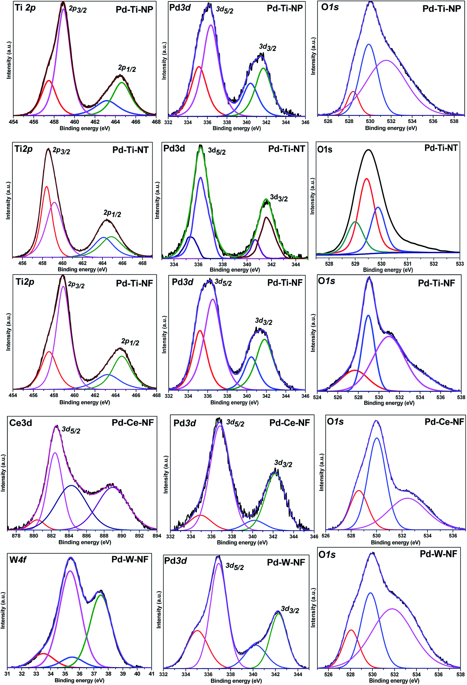 | ||
| Fig. 5 XPS spectra of Pd deposited semiconductor samples. | ||
It has been reported that a pure sample of TiO2 anatase shows mainly a Ti 2p doublet; Ti 2p3/2 BE at 459.2 eV and Ti 2p1/2 BE at 464.3 eV with a BE difference of 5.7 eV. The Ti 2p XP spectra of Pd–Ti-NP, Pd–Ti-NT and Pd–Ti-NT samples showed doublets consisting of two XP peaks. For the Pd-deposited TiO2 nanostructured samples, the Ti 2p XP peaks can be fitted to two components. The Ti 2p3/2 peak at 459 eV was assigned to Ti4+ species and the peak at 457.5 eV was assigned to Ti3+ species.33 These results demonstrate that different proportions of Ti4+ and Ti3+ species are present on the surfaces of the three samples.
The Ce 3d5/2 XP spectrum of the Pd–Ce-NF sample showed XP peaks in the range 877–894 eV.34 The peaks were fitted to four different components at 880.3 eV, 882.4 eV, 884.5 eV and 888.9 eV. The peaks at 882.4 eV and 888.9 eV correspond to Ce(IV) species and the peaks at 880.3 eV and 884.5 eV correspond to Ce(III) species.35 It is very clear from the spectrum that the peak due to Ce(IV) species is more dominant than peaks due other species. It has been reported that W 4f7/2 peaks appear at 37.2 eV, 36.2 eV and 35.2 eV and that W 4f5/2 peaks appear at 35.1 eV, 33.6 eV and 32.9 eV, for W6+, W5+ and W4+ species, respectively.36 The XP spectrum of Pd–W-NF showed W 4f7/2 and W 4f5/2 peaks at 37.5 eV and 35.5 eV and at 35.8 eV and 33.5 eV, respectively. The presence of these peaks confirms the coexistence of W6+ and W5+ species in this sample.
The O 1s spectra of the Pd-deposited semiconductor samples showed three contributions at 527.6–528.6 eV, 529–530 eV and 531–532.5 eV. It has been reported that surface O2−, OH− and H2O species show XP peaks at 530.9 eV, 531.6 eV and 533.5 eV, respectively. In the O 1s spectra, peaks around 529–530 eV and 531–532.5 eV were attributed to lattice oxygen in the semiconductor and surface hydroxyl species, respectively. The minor peak appearing at 527.6–528.6 eV could be due to the oxygen in the interactive Pd–O–M species. As was reported previously, electron exchange between CeO2 and a few Pd atoms at the Pd–CeO2 interface could lead to the formation of ionic Pd species.37 Yu et al.38 reported that Pd2+ ions can link with two unsaturated O2− ions to form O–Pd–O species. The O–Pd–O species could easily interact with Mδ+ species (M = Ti, Ce or W) to form surface Pd–O–M species. The Pd–metal oxide interaction could be promoted by metal oxide species in the reduced state (Ti3+, Ce3+ or W5+), as observed in the catalysts.
Detailed quantitative results from peak-fitting of Pd 3d, Ti 2p, Ce 3d, W 4f and O 1s are presented in Table 3. The bulk and surface elemental composition of the Pd-deposited semiconductor samples was determined by inductively coupled plasma-atomic emission spectroscopy (ICP-AES) and XPS. Pd-deposited samples showed a Pd content of ∼0.25 wt% (slightly lower than the theoretical Pd loading of 0.3 wt%). The surface Pd composition determined by XPS was almost the same as that determined by ICP-AES, confirming that Pd was homogeneously distributed in the samples. The surface concentration of interactive Pd–O–M species, however, varied in different samples. The surface concentration of Pd–O–M species in the Pd–Ce-NF sample was much higher than in the other samples (Table 3).
| Sample | Bulk compositiona (wt%) | Surface compositionb (wt%) | ||||
|---|---|---|---|---|---|---|
| Pd | Ti/Ce/W | O | Pd | Ti/Ce/W | O | |
| a ICP-AES analysis.b XPS analysis.c Percentage of ‘O’ in surface Pd–O–M species. | ||||||
| Pd–Ti-NP | 0.24 | 56.20 | 43.56 | 0.23 | 56.20 | 43.57 (9)c |
| Pd–Ti-NT | 0.25 | 56.56 | 43.19 | 0.23 | 56.56 | 43.21 (14)c |
| Pd–Ti-NF | 0.26 | 57.25 | 42.49 | 0.25 | 57.25 | 42.50 (15)c |
| Pd–Ce-NF | 0.25 | 73.15 | 26.65 | 0.24 | 73.15 | 26.66 (19)c |
| Pd–W-NF | 0.26 | 79.03 | 20.70 | 0.24 | 79.03 | 20.72 (16)c |
3.6 Photocatalytic degradation of p-NP
The photocatalytic performance of the Pd-deposited semiconductors was evaluated by monitoring the degradation of p-NP over several minutes. Blank experiments were conducted to confirm that reaction did not take place in the absence of catalyst or visible light. UV-vis absorbance spectra of p-NP solutions (100 ppm) with different catalysts and different reaction times are shown in Fig. 6. As described above, the catalysts were equilibrated with aqueous p-NP solution to investigate the adsorption of p-NP onto the powdered catalysts. The spectra depicted in Fig. 6 were obtained after equilibration in the dark. Negligible degradation of p-NP was observed under visible light in the absence of catalyst. The UV-vis spectrum of a standard p-NP solution showed a strong absorption band at 317 nm and a weak absorption band at 405 nm. The intensity of these absorption bands weakened and the bands eventually disappeared with increasing reaction time. The activity measurements clearly indicated that degradation of p-NP occurred over all the catalysts. The reduced absorbance of the aqueous p-NP solution after the reaction is attributed to degradation of the aromatic ring present in p-NP.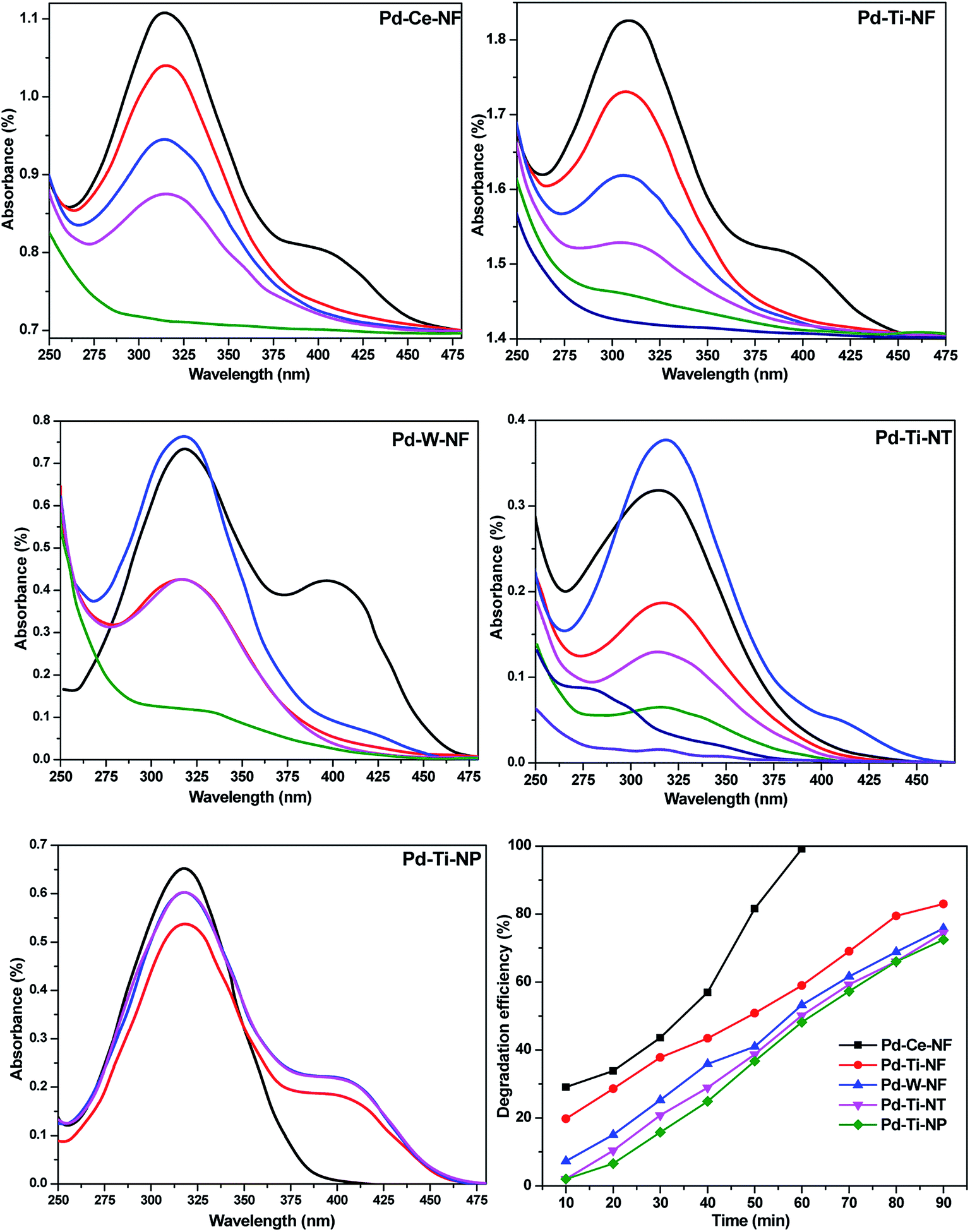 | ||
| Fig. 6 Monitoring the degradation efficiency of catalysts via UV-vis absorption spectroscopy. | ||
Pd–Ce-NF gave almost 99% degradation of p-NP within 60 min, whilst Pd–Ti-NF and Pd–W-NF catalysts gave 90% and 82% degradation after the same reaction time. Pd–Ti-NT and Pd–Ti-NP required 90 and 120 min, respectively, for complete degradation of adsorbed p-NP molecules under similar reaction conditions. The photocatalytic degradation efficiency of the investigated samples was determined using eqn (3). Pd-deposited semiconductors with nanofibrous morphology offered better performance than Pd-deposited TiO2 nanotubes and particles. Out of all the synthesized samples, Pd–Ce-NF was shown to be the best catalyst.
In order to understand the influence of catalyst concentration on photocatalytic activity, the amount of each catalyst was systematically varied. The relationships between degradation efficiency and amount of catalyst are shown in Fig. 7(a). The optimum amount of all catalysts for degradation of p-NP was 0.4 g L−1, except for Pd–W-NF where the optimum amount was 0.5 g L−1. Degradation efficiency increased as the amount of catalyst was increased from 0.2 g L−1 to 0.4 g L−1. As the amount of catalyst in the reactant solution was increased, the number of adsorption sites on the surface increased, allowing greater adsorption of p-NP onto the catalyst surface and increased degradation efficiency. Absorption increased with increasing amounts of catalyst in the reactant solution, likely until the surface was saturated, but degradation efficiency then began to decrease. The probable reason for the decrease in degradation efficiency is that visible light was unable to penetrate the solution and reach the surface in the presence of larger amounts of catalyst.
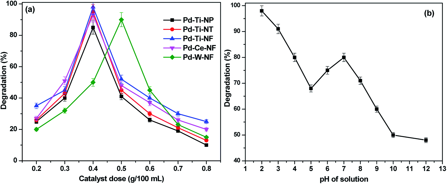 | ||
| Fig. 7 (a) Effect of catalyst amount on p-NP degradation efficiency (b) effect of pH of the p-NP solution over Pd–Ce-NF sample. | ||
Together with the physicochemical properties of the catalyst, the pH of the organic pollutant solution is known to play a crucial role in aqueous phase semiconductor-mediated photocatalytic degradation of p-NP.39 The influence of the pH of the p-NP aqueous solution on the photocatalytic performance of the most active catalyst (Pd–Ce-NF) was studied over the pH range 2.0–12.0. It can be observed that all the catalysts offered better efficiency at lower pH values; maximum efficiency was observed at pH 4.0 (Fig. 7(b)), when almost 98% of the p-NP was degraded after 60 min under visible light. Highly acidic or alkaline solutions were not favorable for complete p-NP degradation because formation of hydroxyl radicals is influenced by the pH of the reactant solution. The pH of the solution also influences the ionic character of the semiconductor surface. For instance, the isoelectric point of CeO2 is 4.43,40 which means that the surface of CeO2 could easily be positively charged at low pH but would be negatively charged at pH > 4.43. The hydroxyl group of p-NP would also be protonated in acidic solution, since the pKa of p-NP is 7.15. The observed results clearly show that protonation of p-NP favors degradation.
To optimize the reaction conditions, the effect of p-NP concentration on degradation was also studied. The p-NP concentration was varied over the range 0.005–0.025 M in the presence of Pd–Ce-NF (0.4 g L−1) at pH 7.0 (Fig. 8). The percentage degradation clearly decreased as the p-NP concentration increased. It was previously observed that, as the p-NP concentration increases, the interaction between HO* species and p-NP becomes weaker and penetration of visible light is decreased. Only a small number of HO* species are then formed, which contributes to the lowered photodegradation efficiency of the catalysts. This behavior can be explained by the fact that photocatalytic reactions generally occur on the surface of the catalyst and the morphology and surface state of semiconductor nanostructures have crucial roles in their photocatalytic activity.
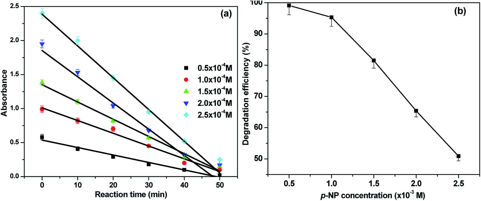 | ||
| Fig. 8 The effect of concentration of p-NP over Pd–Ce-NF catalyst (a) variation of absorbance vs. time (b) variation of degradation efficiency. | ||
Many requirements, including proper band alignment and electronic coupling between the metal nanoparticles and the semiconductor, should be satisfied for electron injection between the metal nanoparticles and the semiconductors. Plasmon-induced resonance energy transfer, however, is not constrained by such requirements.41 It is widely acknowledged that the phenomenon of localized surface plasmon resonance (LSPR) occurs because of interaction between localized electrons of the metal particles (Pd, in this study) with incident visible light.42 Because of LSPR, Pd-deposited semiconductor samples absorbed more light (DR UV-vis spectral data). It appears that the LSPR phenomenon is dependent on the size, local environment and morphology of the particles.43 Leong et al.29 reported that small size Pd nanoparticles (20–30 nm) showed LSPR in the visible region (∼500 nm), which is in agreement with the DR UV-vis spectral results for our synthesized samples.
Plasmon-induced resonance energy transfer depends on near-field enhancement and overlap between the LSPR absorption and the optical transitions in semiconductors. This energy transfer process also localizes the generation of electron–hole pairs mainly near to the metal nanoparticles, which significantly decreases the carrier recombination rate.41 Furthermore, this energy transfer only occurs if the plasmonic metal and semiconductor are in direct contact. In our study, TEM analysis showed that the Pd and semiconductors are in intimate contact with each other. The electrons normally become excited after the semiconductor is exposed to visible light irradiation (Scheme 1). Electrons in the Pd nanoparticles that are excited by LSPR are transferred to the conduction band of the semiconductor, leaving holes in the metal nanoparticles.44 When the Pd nanoparticles have close interactions with the semiconductor, an internal electric field close to the metal–semiconductor interface, known as a Schottky barrier, is generated.45 The internal electric field drives the excited electrons and holes in different directions and the Schottky barrier acts as an electron trap to prevent the backflow of electrons to the semiconductor. The Pd nanoparticles serve as a pool for electrons, thereby catalyzing the reduction of O2. As a result, larger numbers of *OH species are generated and become available on the semiconductor surface where they participate in the degradation of p-NP. Zhang et al. proposed that electron collisions at the metal nanoparticle–semiconductor interface excite electrons from the valence band of the semiconductor to the conduction band, thus generating electron–hole pairs. This group also described the process as an LSPR-powered bandgap breaking effect.46 Clavero observed that photocatalysts with an LSPR-powered bandgap effect absorbed light very efficiently over a wide spectral range and that generating electron–hole pairs often leads to a low carrier recombination rate. These types of photocatalyst thus have the greatest potential for improving the intrinsic limitations of conventional semiconductor photocatalysts.47
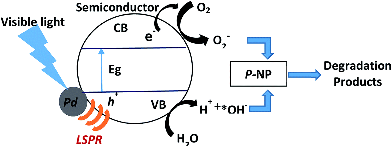 | ||
| Scheme 1 Plausible reaction mechanism of Pd deposited semiconductors for photocatalytic degradation of p-NP. | ||
It was expected that Pd–W-NF would be a more effective photocatalyst than Pd–Ti-NF or Pd–Ce-NF because the smaller band gap would allow better photo absorption in the visible light spectrum by WO3, compared with TiO2 and CeO2.48 However, WO3 has a lower light energy conversion efficiency than TiO2 or CeO2 because the reduction potential is relatively low.49 The surface area of the sample is one of the factors that affects photoactivity. As shown by the N2 physisorption results, the surface area of Pd–Ti-NP (∼74 m2 g−1) is much higher than those of Pd–Ti-NF, Pd–Ce-NF and Pd–W-NF (50 m2 g−1, 35 m2 g−1 and 10 m2 g−1, respectively). Although higher surface area is known to result in a larger capacity to adsorb p-NP, it is important to note that the photocatalytic activity of Pd–Ti-NP was lower than that of Pd–Ce-NF or Pd–Ti-NF, despite its larger surface area. Tuning of photocatalytic activity for a specific semiconductor depends on both structure and morphology and this has been used as a general versatile rationale to design appropriate photocatalysts for different types of reaction.50
The Pd-deposited CeO2 nanofibrous sample had an increased surface-area-to-volume ratio compared with nanofibers of TiO2 and WO3 or nanoparticles and nanotubes of TiO2. This is mainly due to transformation of the nanofibrous CeO2 morphology to a unique ‘mat-like’ morphology (TEM analysis). It appears that this morphology of CeO2 reduces agglomeration of the Pd nanoparticles. The theoretical photocurrent density of the samples was investigated using theoretical calculations and DR UV-vis spectral analysis (ESI†) since the samples displayed absorption profiles at different absorption edges. The photocurrent density is most strongly influenced by the light-harvesting ability and photo charge separation efficiency of the catalyst. The theoretical photocurrent density of Pd–Ce-NF (0.658 mA cm−2) is higher than those of Pd–W-NF (0.559 mA cm−2), Pd–Ti-NF (0.478 mA cm−2), Pd–Ti-NT (0.425 mA cm−2) and Pd–Ti-NP (0.401 mA cm−2), demonstrating the beneficial role of the unique morphology of CeO2 and the size of the Pd particles in the photoactivity.
3.7 Reuse of Pd–CeO2-NF catalyst
Reusability is an important requirement for photocatalysts because use of catalysts for long periods of time leads to significant loss of activity due to agglomeration of particles and photo corrosion. To investigate the reusability of the synthesized samples, the Pd–Ce-NF sample was recycled five times. The degradation efficiency of the sample was 93%, even after five cycles, showing that Pd–Ce-NF could be used as an effective industrial photo catalyst to degrade p-NP. The slight reduction (3%) in degradation efficiency after five cycles could be due to loss of catalyst incurred during the filtration and drying processes.4. Conclusions
A simple deposition–precipitation method was used to synthesize different Pd-deposited semiconductors (TiO2, CeO2 and WO3), with different morphologies (nanoparticles, nanotubes and nanofibers). The obtained materials were used as catalysts for photocatalytic degradation of p-NP under visible light irradiation. Among the Pd-deposited TiO2 samples, TiO2 nanofibers showed better photocatalytic activity than Pd-deposited TiO2 nanoparticles or nanotubes. To explore the advantages of nanofiber morphology, Pd-deposited CeO2 and WO3 nanofiber samples were also tested for photocatalytic activity. Pd-deposited CeO2 nanofibers showed the best performance among all the Pd-deposited semiconductor samples. Elemental analysis, XRD, SEM, TEM, DR UV-vis, N2 physisorption and XPS techniques were used to investigate the role of structural properties on photocatalytic performance. XRD and TEM showed that Pd deposition did not alter the crystal structure of TiO2, WO3 and CeO2 and that Pd was well dispersed on the semiconductor surfaces, with particle sizes < 20 nm. However, Pd deposition resulted in a change in morphology of the CeO2 nanofibers to a unique ‘mat-like’ structure. The presence of small Pd nanoparticles (4 nm) and a high photocurrent density in Pd–Ce-NF is mainly responsible for the high photocatalytic activity. The Pd-deposited samples can be reused at least for five cycles without significant loss of photocatalytic activity.Conflicts of interest
There are no conflicts to declare.References
- A. Fujishima and K. Honda, Nature, 1972, 238, 37–38 CrossRef CAS PubMed.
- K. Koci, L. Obalova, L. Matejova, D. Placha, Z. Lacny, J. Jirkovsky and O. Solcova, Appl. Catal., B, 2009, 89, 494–502 CrossRef CAS.
- M. R. Hoffmann, S. M. Martin, W. Choi and D. W. Bahneman, Chem. Rev., 1995, 95, 69–96 CrossRef CAS.
- J. B. Zhang, Z. Zheng, Y. N. Zhang, J. W. Feng and J. H. Li, J. Hazard. Mater., 2008, 154, 506–512 CrossRef CAS PubMed.
- K. Vignesh, R. Priyanka, R. Hariharan, M. Rajarajan and A. Suganthi, J. Ind. Eng. Chem., 2014, 20, 435–443 CrossRef CAS.
- A. Zielinska-Jurek and J. Hupka, Catal. Today, 2014, 230, 181–187 CrossRef CAS.
- M. N. Chong, B. Jin, C. W. K. Chow and C. Saint, Water Res., 2010, 44, 2997–3027 CrossRef CAS PubMed.
- D. Li, H. Haneda, N. K. Labhsetwar, S. Hishita and N. Ohashi, Chem. Phys. Lett., 2005, 401, 579–584 CrossRef CAS.
- H. Widiyandari, A. Purwanto, R. Balgis, T. Ogi and K. Okuyama, Chem. Eng. J., 2012, 180, 323–329 CrossRef CAS; V. Subramanian, E. E. Wolf and P. V. Kamat, J. Am. Chem. Soc., 2004, 126, 4943–4950 CrossRef PubMed.
- J. Liqiang, W. Baiqi, X. Baifu, L. Shudan, S. Keying, C. Weimin and F. Honggang, J. Solid State Chem., 2004, 177, 4221–4227 CrossRef.
- S. K. Mohapatra, N. Kondamudi, S. Banerjee and M. Misra, Langmuir, 2008, 24, 11276–11281 CrossRef CAS PubMed.
- B. S. Kwak, J. Chae, J. Kim and M. Kang, Bull. Korean Chem. Soc., 2009, 30, 1047–1053 CrossRef CAS.
- Z. Xiong, L. Zhang and X. Song Zhao, Chem.–Eur. J., 2014, 20, 14715–14720 CrossRef CAS PubMed.
- N. Q. Long, N. T. T. Uyen, D. T. Hoang and D. B. Trung, International journal of renewable energy and environmental engineering, 2015, 3, 52–55 Search PubMed.
- H. G. Lee, S. A. Gopalan, K. Shanmugasundaram, A. I. Gopalan, S. W. Kang and K. P. Lee, J. Hazard. Mater., 2015, 283, 400–409 CrossRef CAS PubMed.
- F. Lei and B. Yan, J. Phys. Chem. C, 2009, 113, 1074–1082 CAS.
- J. G. Yu, Y. R. Su and B. Cheng, Adv. Funct. Mater., 2007, 17, 1984–1990 CrossRef CAS.
- J. Yu, H. Yu, H. Guo, M. Li and S. Mann, Small, 2008, 4, 87–91 CrossRef CAS PubMed.
- N. Zhang, S. Liu, X. Fu and Y.-J. Xu, J. Phys. Chem. C, 2011, 115, 22901–22909 CAS.
- E. Hosono, S. Fujihara, H. Imai, I. Honma, I. Masaki and H. Zhou, ACS Nano, 2007, 1, 273–278 CrossRef CAS PubMed.
- Y. Suzuki, M.-H. Berger, D. D'Elia, P. Ilbizian, C. Beauger, A. Rigacci, J.-F. Hochepied and P. Achard, Nano, 2008, 3, 1–7 CrossRef.
- J. M. Campelo, D. Luna, R. Luque, J. M. Marinas and A. Romero, ChemSusChem, 2009, 2, 18–45 CrossRef CAS PubMed.
- G. K. Alqurashi, A. Al-Shehri and K. Narasimharao, RSC Adv., 2016, 6, 71076–71091 RSC.
- T. Kasuga, M. Hiramatsu, A. Hoson, T. Sekino and K. Niihara, Langmuir, 1998, 14, 3160–3163 CrossRef CAS.
- R. Gopinath, K. Narasimharao, P. S. Saiprasad, S. S. Madhavendra, S. Narayana and G. Vivekanandan, J. Mol. Catal. A: Chem., 2002, 181, 215–220 CrossRef CAS.
- Y. Zhang, N. Zhang, Z.-R. Tang and Y.-J. Xu, ACS Sustainable Chem. Eng., 2013, 1, 1258–1266 CrossRef CAS.
- S. Zhang, C. Chen, M. Cargnello, P. Fornasiero, R. J. Gorte, G. W. Graham and X. Pan, Nat. Commun., 2015, 6, 7778–7784 CrossRef PubMed.
- N. Zhang, S. Q. Liu, X. Z. Fu and Y. J. Xu, J. Phys. Chem. C, 2011, 115, 9136–9145 CAS.
- K. H. Leong, H. Y. Chu, S. Ibrahim and P. Saravanan, Beilstein J. Nanotechnol., 2015, 6, 428–437 CrossRef CAS PubMed.
- J. Ding, Z. Huang, J. Zhu, S. Kou, X. Zang and H. Yang, Sci. Rep., 2015, 5, 17773 CrossRef CAS PubMed.
- N. Horzum, R. Muñoz-Espí, G. Glasser, M. M. Demir, K. Landfester and D. Crespy, ACS Appl. Mater. Interfaces, 2012, 4, 6338–6345 CAS.
- G. Cristoforetti, E. Pitzalis, R. Spiniello, R. Ishak, F. Giammanco, M. Muniz Miranda and S. Caporali, Appl. Surf. Sci., 2012, 258, 3289–3297 CrossRef CAS.
- Handbook of X-Ray Photoelectron Spectroscopy, ed. C. D. Wagner, W. M. Riggs, L. E. Davis, J. F. Moudler, and G. E. Muilenberg, Perkin-Elmer, 1992, p. 73 Search PubMed.
- G. J. Wang, Y. Guo and G. Z. Lu, Fuel Process. Technol., 2015, 130, 71–77 CrossRef CAS.
- P. A. P. Nascente, S. S. Maluf, C. R. M. Afonso, R. Landers, A. N. Pinheiro and E. R. Leite, Appl. Surf. Sci., 2014, 315, 490–498 CrossRef CAS.
- I. M. Szilágyi, B. Fórizs, O. Rosseler, Á. Szegedi, P. Németh, P. Király, G. Tárkányi, B. Vajna, K. Varga-Josepovits, K. László, A. L. Tóth, P. Baranyai and M. Leskelä, J. Catal., 2012, 294, 119–127 CrossRef.
- N. Zhang and Y.-J. Xu, Chem. Mater., 2013, 25, 1979–1988 CrossRef CAS.
- Y. Yu, T. He, L. Guo, Y. Yang, L. Guo, Y. Tang and Y. Cao, Sci. Rep., 2015, 5, 9561–9566 CrossRef CAS PubMed.
- N. San, A. H. Lu, G. Koçtürk and Z. Çinar, J. Photochem. Photobiol., A, 2002, 146, 189–197 CrossRef CAS.
- J. Mao, Y. Bai, L. Gu, P. A. van Aken and M. J. Tu, J. Nanopart. Res., 2010, 12, 2045–2049 CrossRef CAS.
- X.-C. Ma, Y. Dai, L. Yu and B.-B. Huang, Light: Sci. Appl., 2016, 5, e16017 CrossRef CAS.
- E. Hutter and J. H. Fendler, Adv. Mater., 2004, 16, 1685–1706 CrossRef CAS.
- C. Noguez, J. Phys. Chem. C, 2007, 111, 3806–3819 CAS.
- I. Díez and R. H. A. Ras, Nanoscale, 2011, 3, 1963–1970 RSC.
- J. Ohyama, A. Yamamoto, K. Teramura, T. Shishido and T. Tanaka, ACS Catal., 2011, 1, 187–192 CrossRef CAS.
- X. M. Zhang, Y. L. Chen, R. S. Liu and D. P. Tsai, Rep. Prog. Phys., 2013, 76, 046401 CrossRef PubMed.
- C. Clavero, Nat. Photonics, 2014, 8, 95–103 CrossRef CAS.
- W. Morales, M. Cason, O. Aina, N. R. De Tacconi and K. Rajeshwar, J. Am. Chem. Soc., 2008, 130, 6318–6319 CrossRef CAS PubMed.
- H. Kim, K. Senthil and K. Yong, Mater. Chem. Phys., 2010, 120, 452–455 CrossRef CAS.
- X. Wang and R. A. Caruso, J. Mater. Chem., 2011, 21, 20–28 RSC.
Footnote |
| † Electronic supplementary information (ESI) available. See DOI: 10.1039/c7ra11080d |
| This journal is © The Royal Society of Chemistry 2017 |