
 Open Access Article
 This Open Access Article is licensed under a Creative Commons Attribution-Non Commercial 3.0 Unported Licence
Control of the intrinsic microstructure in AP-PECVD synthesised amorphous silica thin films
F. M. Elam *abc,
B. C. A. M. van der Velden-Schuermansa,
S. A. Starostina,
M. C. M. van de Sandenbc and
H. W. de Vries*c
*abc,
B. C. A. M. van der Velden-Schuermansa,
S. A. Starostina,
M. C. M. van de Sandenbc and
H. W. de Vries*c
aFUJIFILM Manufacturing Europe B.V., P.O. Box 90156, 5000 LJ Tilburg, The Netherlands. E-mail: f.m.elam@differ.nl
bEindhoven University of Technology, Applied Physics, P.O. Box 513, 5600 MB Eindhoven, The Netherlands
cDIFFER – Dutch Institute for Fundamental Energy Research, P.O. Box 6336, 5600 HH Eindhoven, The Netherlands. E-mail: h.w.devries@differ.nl
First published on 10th November 2017
Abstract
Amorphous single layered silica films deposited using industrially scalable roll-to-roll atmospheric pressure-plasma enhanced chemical vapor deposition were evaluated in terms of structure–performance relationships. Polarised attenuated total reflectance-Fourier transform infrared absorption spectroscopy and heavy water exposure to induce hydrogen–deuterium exchange revealed it was possible to control the film porosity simply by varying the precursor flux and plasma residence times. Denser silica network structures with fewer hydroxyl impurities, shorter Si–O bonds, decreased Si–O–Si bond angles and a greater magnitude of isolated pores were found in films deposited with decreased precursor flux and increased plasma residence times, and consequently exhibited significantly improved encapsulation performance.
Introduction
The economical manufacture of thin functional films with precisely controlled porosity is of particular importance for industries involved in gas separation, water purification, and the protection of flexible electronics, the latter of which this work is focussed on.Flexible encapsulation barriers are designed primarily to protect electronic devices such as solar cells against degradation from oxygen and water,1–9 thus prolonging device lifetimes and improving operational stability. A widely regarded material for such a barrier is amorphous silica, which can be deposited onto flexible polymer substrates using a variety of different deposition methods.2,10–21 One particularly cost-effective and thus industrially relevant method, is atmospheric pressure-plasma enhanced chemical vapour deposition (AP-PECVD). The absence of any large footprint vacuum equipment,9 and potential for continuous processing, makes it an ideal technology for the large scale manufacture of flexible protective coatings.9–12,22
It was discovered recently that encapsulation performance could be improved for amorphous silica films deposited onto flexible polymer substrates using industrially scalable roll-to-roll AP-PECVD, by increasing the deposition input energy per precursor gas molecule (a parameter that relates increasing plasma residence time with decreasing precursor vapour flow rates, whilst maintaining a constant power dissipation in the discharge).10,12 X-ray photoelectron spectroscopy (XPS) was used to successfully determine the elemental composition and hence approximate O![[thin space (1/6-em)]](https://www.rsc.org/images/entities/char_2009.gif) :Si ratio of the films.10,12 Unfortunately in these instances, XPS was unable to provide a sufficiently detailed insight into the changes in the silica network structure as a function of deposition input energy, and hence the impact this had upon the encapsulation performance of the films.
:Si ratio of the films.10,12 Unfortunately in these instances, XPS was unable to provide a sufficiently detailed insight into the changes in the silica network structure as a function of deposition input energy, and hence the impact this had upon the encapsulation performance of the films.
Attenuated total reflectance-Fourier transform infrared (ATR-FTIR) absorption spectroscopy with an un-polarised light source was therefore used as an alternative, to study the intrinsic microstructure of these amorphous silica films, with focus on the extent of hydroxyl (–OH) impurities.10,12,23–27 It was shown that an improved encapsulation performance was due in part to a decrease in concentration of network disrupting silanol (Si–OH) groups, thus implying that the microstructure of the silica lattice increased in density at higher specific deposition energies per precursor molecule.10,12 However, no direct detailed analysis of the Si–O–Si bonding was carried out to verify this assumption. Fortunately, this type of bonding can be resolved by performing ATR-FTIR absorption spectroscopy using a polarised light source.
However, ATR-FTIR analysis alone does not provide a complete representation of the degree of porosity within the silica films. Ellipsometric porosimetry (EP) and electrical impedance spectroscopy (EIS) were two alternative techniques used extensively by Perrotta et al. to very effectively characterise the nano-porosity, the pore size range and the presence of macroscale defects in the structure of silica layers.28–31 Due to the nature of these techniques, however, the majority of the analysis was performed on samples deposited upon rigid silicon wafers, rather than flexible polymer substrates. A full characterisation of the nano-pore content of silica layers was unfortunately found to be problematic using EP if a polyethylene terephthalate substrate was used.31
A method unhindered by the composition of the substrate material, and therefore an alternative to EP and EIS, is a technique involving proton exchange via exposure to heavy water (D2O) and subsequent detection of said transfer using ATR-FTIR, highlighted relatively recently by Liu et al.32 This method can provide information relating to the total pore surface area and the extent of closed porosity. It is therefore possible, by using this procedure, to obtain a more comprehensive interpretation of the bonding arrangements in amorphous silica films deposited on polymer substrates using AP-PECVD.
The ability to economically produce functional films with a specific porosity would be highly advantageous in the encapsulation barrier market. Therefore, understanding the influence roll-to-roll AP-PECVD processing has upon the intrinsic microstructure (namely the Si–O–Si bonding and degree of closed porosity), and resulting encapsulation performance of the synthesised amorphous silica layers is of paramount interest, and hence forms the basis of this work. Focus will be placed on the utilisation of two complementary analytical techniques known to be suitable for the structural analysis of films deposited upon polymeric substrate materials, namely polarised ATR-FTIR and hydrogen–deuterium exchange.
Experimental section
Single layer amorphous silica-like films were deposited onto thermally stabilised optical grade polyethylene 2,6 naphthalate (PEN) foil (Teonex Q65FA, Teijin DuPont Films) with a width and thickness of 180 mm and 100 μm respectively, using a glow-like AP dielectric barrier discharge in an industrially scalable roll-to-roll set-up open to ambient air. A schematic representation of the AP-PECVD reactor is shown in Fig. 1 and all basic device and thin film deposition parameters can be found in a recent publication by Elam et al.12 The reactor itself is in an ISO class 3 cleanroom, in accordance with ISO 14644-1 standards.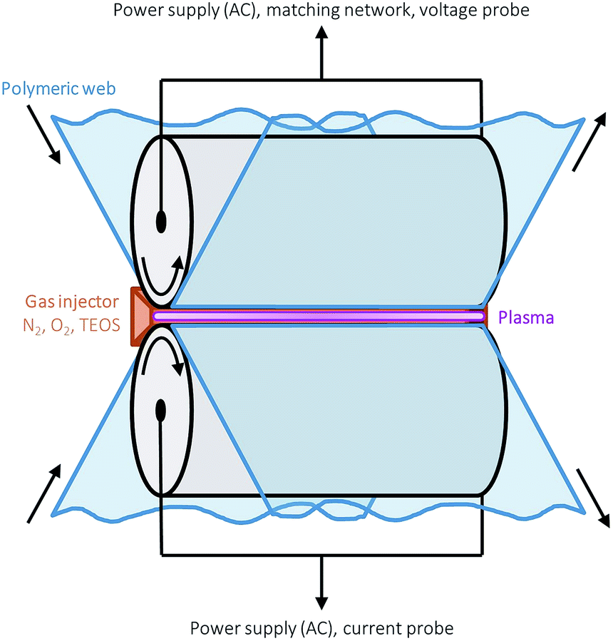 | ||
| Fig. 1 Schematic of the roll-to-roll glow-like atmospheric pressure dielectric barrier discharge used for the deposition of all silica films by means of plasma enhanced chemical vapour deposition. | ||
The PEN foil was positioned over the lower drum electrode and the foil transport speed was varied from 133–33 mm min−1 to enable the deposition of uniform ∼150 nm barrier layers. A 63 μm thick sacrificial polymer, polyethylene terephthalate (PET) (ASTERATM Functional Foils, AGFA), was used as the dielectric material for the upper drum electrode, with foil transport speed maintained at 50 mm min−1 in all cases. The reactant gases for every deposition were oxygen (technical grade) and tetraethyl orthosilicate (Si(OC2H5)4, TEOS) (≥99.0%, Sigma-Aldrich). The precursor gas, TEOS, was injected via a controlled evaporation mixer unit (CEM-Technology, Bronkhorst HIGH-TECH B.V.), where the liquid precursor was combined with 1 slm argon (technical grade). The carrier gas in all cases was nitrogen (technical grade), with a flow of 20 slm. All four gases were mixed before being released into the plasma. In order to vary the specific input energy per TEOS molecule and therefore the layer densities for the 150 nm barrier layers, the TEOS and oxygen gas flows were adjusted with a fixed ratio of 4.5 × 10⁻³ in the range of 7.2 × 10⁻³ to 1.8 × 10⁻³ slm and 1.6–0.4 slm respectively. This resulted in the deposition of barrier layers with input energies ranging from approximately 1.4–4.9 keV per TEOS molecule. A description of the method used to calculate the input energy per TEOS molecule (E per TEOS) is outlined in a publication by Elam et al.12
Spectroscopic ellipsometry (SE) was performed using a variable angle spectroscopic ellipsometer (M-2000D, J.A. Woollam Co. Inc.) in the wavelength range of 400–1000 nm in order to ensure that the single layer barriers post-deposition were of the expected thickness and demonstrated good overall uniformity.33 The Cauchy dispersion function was used to model the PEN substrate and the silica-like thin films as two separate entities. The optical model did not take into account the substrate anisotropy;14 however sample orientation was consistent for each measurement.
The effective WVTR of the single layer samples comprising barrier and substrate layers were determined using a Deltaperm (Technolox Ltd.), with set conditions of 40 °C, 90% relative humidity (RH). This measurement therefore took into account the overall permeation of the films; including contributions from macro-defects (>1 nm), and the intrinsic microstructure (nano-defects (0.3–1 nm) and gas transport through the amorphous silica-like lattice itself (0.2–0.3 nm)).17 The Deltaperm fulfils the ASTM D 1434-82 (2003) standard for permeation measurements, and has a WVTR limit of 2 × 10⁻⁴ g m−2 day−1. Sample areas of 50 cm2 were investigated, with each measurement lasting for 60–190 h depending on encapsulating ability, in order to ensure the permeation rate had stabilised. The WVTR was recorded each minute, and calculated as summarised in ref. 12. From the Deltaperm measurements, data concerning the lag-time (the time taken for the WVTR to reach a steady-state) was also obtained, and from this the apparent diffusion coefficient of the encapsulation layers calculated as outlined in ref. 12. It should be noted that all barrier layers used for the encapsulation performance measurements showed excellent adhesion to the polymeric substrate. No evidence of delamination was observed after evaluation using a cross-cut tape adhesion test (in accordance with ISO 2409:2003).10
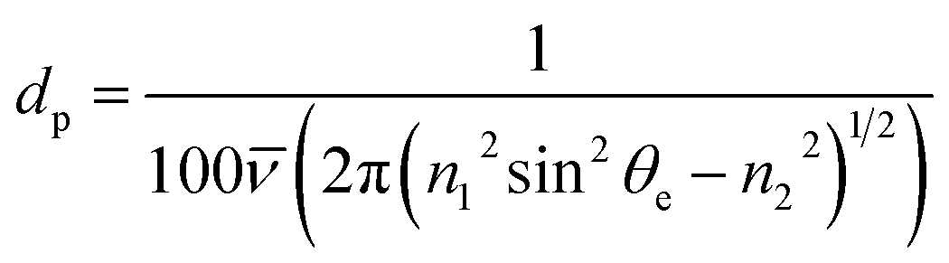
Attenuated total reflectance-Fourier transform infrared (ATR-FTIR) absorption spectroscopy was performed using s-polarised light (Frontier FT-IR/FIR Spectrometer, PerkinElmer; VeeMAX III Accessory, PIKE Technologies) to investigate the average chemical structure of the barrier layers,34 with particular focus upon the Si–O–Si stretching modes. This set-up utilised a Ge crystal with a 60° face angle and one internal reflection. Spectra were obtained at a set angle of 60° (and hence a 60° effective angle θe), which resulted in a penetration depth dp range of 391–678 nm for the selected wavenumber range of 1300–750 cm−1, calculated using eqn (1),35
 | (1) |
![[small nu, Greek, macron]](https://www.rsc.org/images/entities/i_char_e0ce.gif) is the wavenumber, n1 is the refractive index of the Ge crystal (4.0) and n2 is the refractive index of the silica layer (1.48). To minimise the effect of background noise, 16 scans were acquired for every measurement. The absorption spectrum of the substrate was subtracted from each sample spectrum. In addition, every sample spectrum was normalised to the Si–O–Si asymmetric stretch peak centred at approximately 1050 cm−1, and interpreted assuming that an increase in peak absorption intensity equated to an increase in the presence of the corresponding functional group. Deconvolution of all spectral peaks was carried out (Peak Analyzer – Fit Peaks (Pro), OriginPro 9.1) in order to determine the position, full width at half maximum (FWHM) and intensity of each elementary contribution. For the purpose of this analysis, a separate set of samples were investigated as the PEN substrate has strong IR absorption peaks in the spectral region of interest for silica-like film evaluation. Therefore, a set of equivalent barrier layer-type films that had been deposited onto a PET substrate pre-coated with a 1 μm thick layer of polyvinylidene chloride (PVDC) were analysed instead. The PVDC layer was thick enough to prevent penetration of the IR evanescent wave into the underlying PET substrate, and its FTIR absorption spectrum neutral enough not to impede the absorption spectrum of the silica layers, thereby ensuring ‘clean’ spectra of the films could be obtained. All equivalent barrier layer-type films were ∼200 nm in thickness, as it is known, especially when using polarised light, that both the FTIR absorption peak positions and FWHM can vary as a function of film thickness.36–40
is the wavenumber, n1 is the refractive index of the Ge crystal (4.0) and n2 is the refractive index of the silica layer (1.48). To minimise the effect of background noise, 16 scans were acquired for every measurement. The absorption spectrum of the substrate was subtracted from each sample spectrum. In addition, every sample spectrum was normalised to the Si–O–Si asymmetric stretch peak centred at approximately 1050 cm−1, and interpreted assuming that an increase in peak absorption intensity equated to an increase in the presence of the corresponding functional group. Deconvolution of all spectral peaks was carried out (Peak Analyzer – Fit Peaks (Pro), OriginPro 9.1) in order to determine the position, full width at half maximum (FWHM) and intensity of each elementary contribution. For the purpose of this analysis, a separate set of samples were investigated as the PEN substrate has strong IR absorption peaks in the spectral region of interest for silica-like film evaluation. Therefore, a set of equivalent barrier layer-type films that had been deposited onto a PET substrate pre-coated with a 1 μm thick layer of polyvinylidene chloride (PVDC) were analysed instead. The PVDC layer was thick enough to prevent penetration of the IR evanescent wave into the underlying PET substrate, and its FTIR absorption spectrum neutral enough not to impede the absorption spectrum of the silica layers, thereby ensuring ‘clean’ spectra of the films could be obtained. All equivalent barrier layer-type films were ∼200 nm in thickness, as it is known, especially when using polarised light, that both the FTIR absorption peak positions and FWHM can vary as a function of film thickness.36–40
The pore interconnectivity within the 150 nm silica-like barrier layers deposited on PEN, was determined by means of exposure to deuterium oxide (D2O) (Sigma-Aldrich) and subsequent detection of hydrogen–deuterium (1H–2H, H–D) exchange using un-polarised ATR-FTIR absorption spectroscopy (Frontier FT-IR/FIR Spectrometer, PerkinElmer; Frontier UATR Ge/Ge, PerkinElmer). This accessory similarly used a Ge crystal with one internal reflection, but a 45° face angle. Spectra were acquired at a fixed angle of 45°, which resulted in a penetration depth range of 176–330 nm for the selected wavenumber range of 3750–2000 cm−1 (calculated as before using eqn (1)) and thus improved the detection and subsequent analysis of SiO–H and H–OH spectral peaks. The full procedure comprised drying the samples in a desiccator under vacuum for one week, followed by exposure to D2O for one week using a climate chamber, with set conditions of 40 °C, 90% RH. Samples were then dried again for one week in a desiccator under vacuum and finally exposed to ambient air for one week. ATR-FTIR absorption spectra were recorded directly after every step.
Results and discussion
Encapsulation performance
The effective WVTR trend (at 40 °C, 90% RH) with respect to increasing input energy per TEOS molecule (a parameter that relates increasing plasma residence time, or substrate transport speed, with decreasing TEOS vapour flow rates, whilst maintaining a constant power dissipation in the discharge) during the deposition of the 150 nm barrier layer is shown in Fig. 2a. As previously reported, a clear correlation can be observed between increasing input energy per TEOS molecule and decreasing effective WVTR, suggesting that the encapsulation properties of silica-like films deposited using AP-PECVD improve as a function of increased deposition input energy.10 However, this improvement is unfortunately limited by the formation of macro-defects that occur as a result of the gradually intensified processing conditions required to achieve deposition input energies greater than 6 keV per TEOS for single layered films and 20 keV per TEOS for bilayer films.12,13 Fig. 2b that illustrates the lag-time and apparent diffusion coefficient of the single layer barrier as a function of input energy per TEOS molecule, complements the WVTR data, reaffirming the above statements that encapsulation performance improves to a certain extent with increasing input energy per TEOS molecule during the deposition process.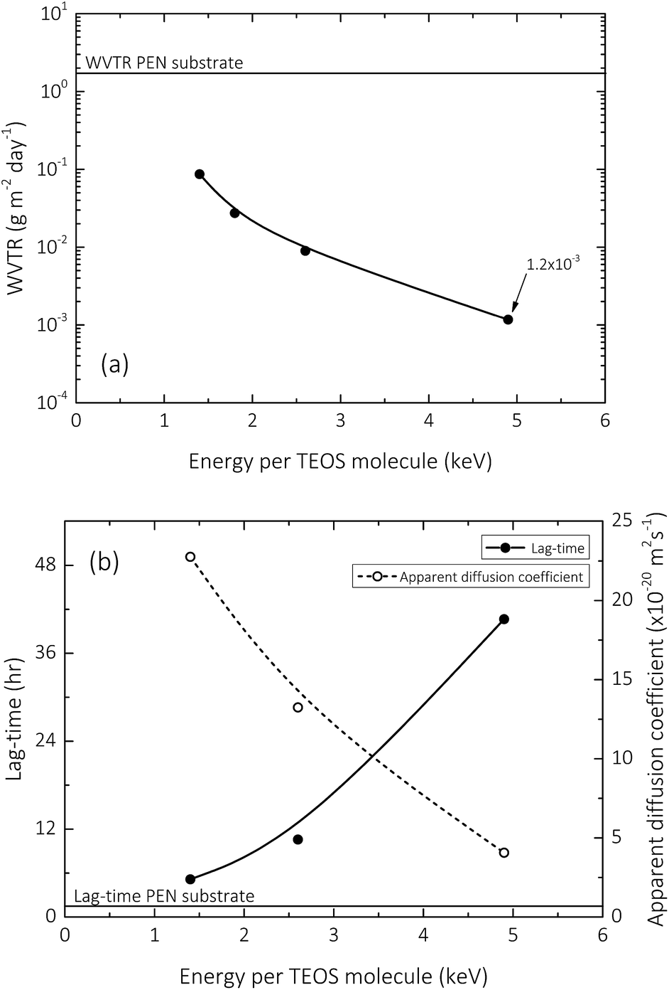 | ||
| Fig. 2 Water permeation measurements (at 40 °C, 90% relative humidity): (a) water vapour transmission rate with respect to increasing input energy per TEOS molecule for synthesis of a 150 nm barrier layer; (b) lag-time and corresponding apparent diffusion coefficient with respect to increasing input energy per TEOS molecule for synthesis of a 150 nm barrier layer. | ||
Silica network structure: polarised ATR-FTIR spectroscopy
Fig. 3 and 4 show the normalised s-polarised ATR-FTIR absorption spectra and subsequent deconvolution, of the amorphous silica barrier layers deposited by AP-PECVD, with particular focus upon the Si–O–Si stretching modes. The presence of the silanol (Si–OH) group in amorphous silica deposited using AP-PECVD is discussed in greater detail in a recent publication by Elam et al.12 For the purpose of understanding the extent and nature of the variation in film structure as a function of increasing input energy per TEOS molecule during the deposition process, the data set was extended to include samples deposited at energies up to 70 keV per TEOS molecule.12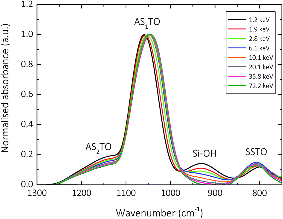 | ||
| Fig. 3 Normalised s-polarized ATR-FTIR absorption spectra showing: the Si–O–Si transverse optical symmetric stretch (SSTO, ∼800 cm−1); the silanol stretch (Si–OH, 930 cm−1); the Si–O–Si transverse optical asymmetric stretch with adjacent O atoms in phase (AS1TO, ∼1050 cm−1); and the Si–O–Si transverse optical asymmetric stretch with adjacent O atoms 180° out of phase (AS2TO, ∼1160 cm−1) of 200 nm silica-like thin films deposited with input E per TEOS from 1.2–72.2 keV onto a modified PET substrate using AP-PECVD, under conditions replicating those of the barrier layer synthesis. | ||
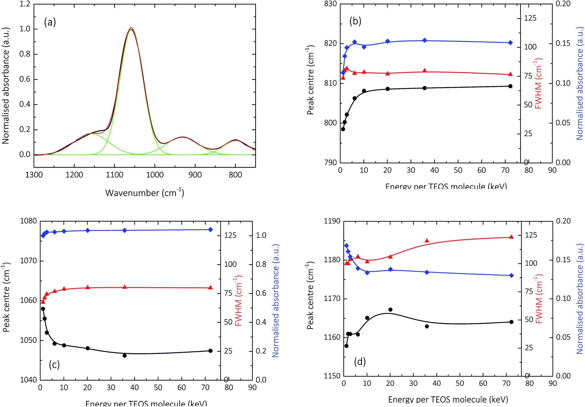 | ||
| Fig. 4 Deconvolution (a) of the normalised s-polarized ATR-FTIR absorption spectra shown in Fig. 3 illustrating the specific peak centre (black; circle), FWHM (red; triangle) and absorbance (blue; diamond) as a function of increasing input E per TEOS for the synthesis of the barrier layer for: (b) Si–O–Si SSTO; (c) Si–O–Si AS1TO and (d) Si–O–Si AS2TO. | ||
Amorphous silica, unlike conventional crystalline silicon dioxide (SiO2), does not possess a silicon–oxygen (Si–O) microstructure with obvious long range order.39,41 The crystal symmetry is broken by disordered linkage, and by the existence of oxygen atoms that are not shared among neighbouring tetrahedra. This disorder therefore gives rise to localisation, and hence the vibrational properties of amorphous silica are usually interpreted in terms of Si–O–Si subunits.41 However, due to its lattice-like network structure, longitudinal optical (LO) and transverse optical (TO) phonons associated with the Si–O–Si symmetric (SS) and asymmetric stretching (AS) modes also exist.42–44 It is possible to activate the LO modes with a transition dipole moment oriented perpendicular to the surface of the film,45,46 by utilising the p-polarised component of IR light in oblique-incidence reflectance.46–48
In a similar fashion, TO modes oriented parallel to the surface,45,46 are activated alongside LO modes, but can be isolated by using s-polarised light.48 Furthermore, the Si–O–Si asymmetric stretching mode in fact generates two vibrational modes: the AS1 mode whereby adjacent oxygen atoms execute the asymmetric stretching motion in phase with one another, and the AS2 mode characteristic of the Si–O–Si shoulder peak, in which adjacent oxygen atoms perform the asymmetric stretch 180° out of phase.49–51 This therefore results in six IR active modes associated with the Si–O–Si functional group; namely the TO and LO phonons for the symmetric stretch (SSTO and SSLO), and the TO and LO phonons for both asymmetric stretches (AS1TO, AS2TO, AS1LO and AS2LO).51
The most prominent peaks in the normalised s-polarised ATR-FTIR absorption spectrum of amorphous silica shown in Fig. 3 can be assigned to the Si–O–Si SSTO mode (∼800 cm−1), the silanol (Si–OH) stretch (930 cm−1), the Si–O–Si AS1TO mode (∼1050 cm−1) and the Si–O–Si AS2TO mode (∼1160 cm−1). It should be highlighted that no peaks at 1275 cm−1 due to the bending mode of methyl groups in Si–CH3 are observed,24,52–54 indicating that all silica-like films deposited using the AP-PECVD process are essentially carbon free. This assumption has also been verified by prior XPS analysis, which revealed the maximum percentage of elemental carbon present in the silica layers was 3.5%.10,12
Several clear trends become apparent upon deconvolution (Fig. 4) of the spectra shown in Fig. 3. The absorbance of the SSTO mode increases with increasing input energy per TEOS molecule during the deposition process. According to the Beer–Lambert law,12 this implies an increase in concentration of Si–O–Si species and thus reduction in the porosity of the intrinsic microstructure of the silica network as a function of increasing deposition input energy. Contrary to this, however, the absorbance of the AS2TO vibrational mode decreases. An increase in the intensity of the AS2TO mode has been previously associated with disorder-induced mechanical coupling to the AS1 mode,50,51,55 increased porosity in the layer,56 and increased disorder in the silica microstructure.25,27,50,55 Therefore a decrease in the intensity of the AS2TO vibrational mode would also indicate a reduction in porosity and hence densification of the intrinsic microstructure of the silica network.
The peak FWHM, widely acknowledged to be indicative of the degree of variation in bonding arrangements surrounding a particular functional group,50,57–59 can be seen to increase for all Si–O–Si stretching modes, as the deposition input energy increases. As the intrinsic silica network densifies with a reduction in the concentration of network-disrupting silanol groups,12 the distribution of Si–O–Si bond angles in the network is likely to increase, thereby resulting in an increase in the FWHM.23,60 The greater distribution of bond angles may also coincide with an increase in bond strain and thus film tensile stress.61
The specific peak centres of the SSTO and AS2TO vibrations are observed to increase in wavenumber with increasing film density,62 most likely the consequence of an increase in the force constant k, of the Si–O–Si bonds since the reduced mass of the vibrating atoms μ, remains unchanged.63 Due to the removal of network-disrupting Si–OH groups,12 the length of Si–O bonds are liable to decrease, resulting in an increase in bond strength and thus rise in vibrational frequency as a function of increasing deposition input energy. Conversely, the specific peak centre of the AS1TO vibrational mode is quite visibly seen to decrease in wavenumber as a function of increasing input energy per TEOS molecule and hence reduction in porosity. This effect was also previously observed in conjunction with removal of hydroxyl species,23,60 and densification.62 Slight variations in peak positions can also be attributed to changes in the intrinsic bond angles, as described in eqn (2), which is specific for the Si–O–Si vibration:
 | (2) |
Therefore the presented ATR-FTIR analysis suggests that the intrinsic micro-structure of AP-PECVD synthesised amorphous silica densifies as a function of increasing deposition input energy. The densification is confirmed by an increase in the presence of Si–O–Si groups due to removal of hydroxyl species,12 a decrease in Si–O bond lengths and decrease in Si–O–Si bond angle which may in turn result in increased bond strain. The findings suitably confirm the improved encapsulation performance observed as a function of increasing deposition input energy shown in Fig. 2.
However, as illustrated in Fig. 4b–d, the silica network regarding the Si–O–Si bonding appears to rapidly densify and then plateau at deposition input energies of approximately 6–10 keV per TEOS. This does not entirely coincide with the prior reported ATR-FTIR analysis focussed on the hydroxyl content of the films,12 which showed a more gradual removal of silanol impurities as a function of deposition input energy up to at least ∼35 keV per TEOS. This finding would imply that a potential two-part densification process occurs as a function of increasing deposition input energy for amorphous silica films synthesised using AP-PECVD. First, rapid densification of the silica network takes place, alongside the steady removal of hydroxyl impurities for films synthesised at specific deposition E per TEOS up to ∼6 keV. The silica network then continues to densify, but at a much slower rate, in line with the gradual to almost complete removal of hydroxyl impurities only seen for films deposited at specific energies greater than ∼35 keV per TEOS.12
Pore interconnectivity: hydrogen–deuterium exchange
The influence of the D2O exposure process performed to understand pore interconnectivity in the 150 nm silica-like thin films can be seen in the normalised un-polarised ATR-FTIR absorption spectra shown in Fig. 5. Hydrogen–deuterium exchange, due to the increase in reduced mass of the vibrating atoms μ, induces a detectable decrease in the frequency of the O–H vibration.63 This is clearly evident for all films upon exposure to D2O, and is seemingly reversible upon subsequent drying and contact with ambient air.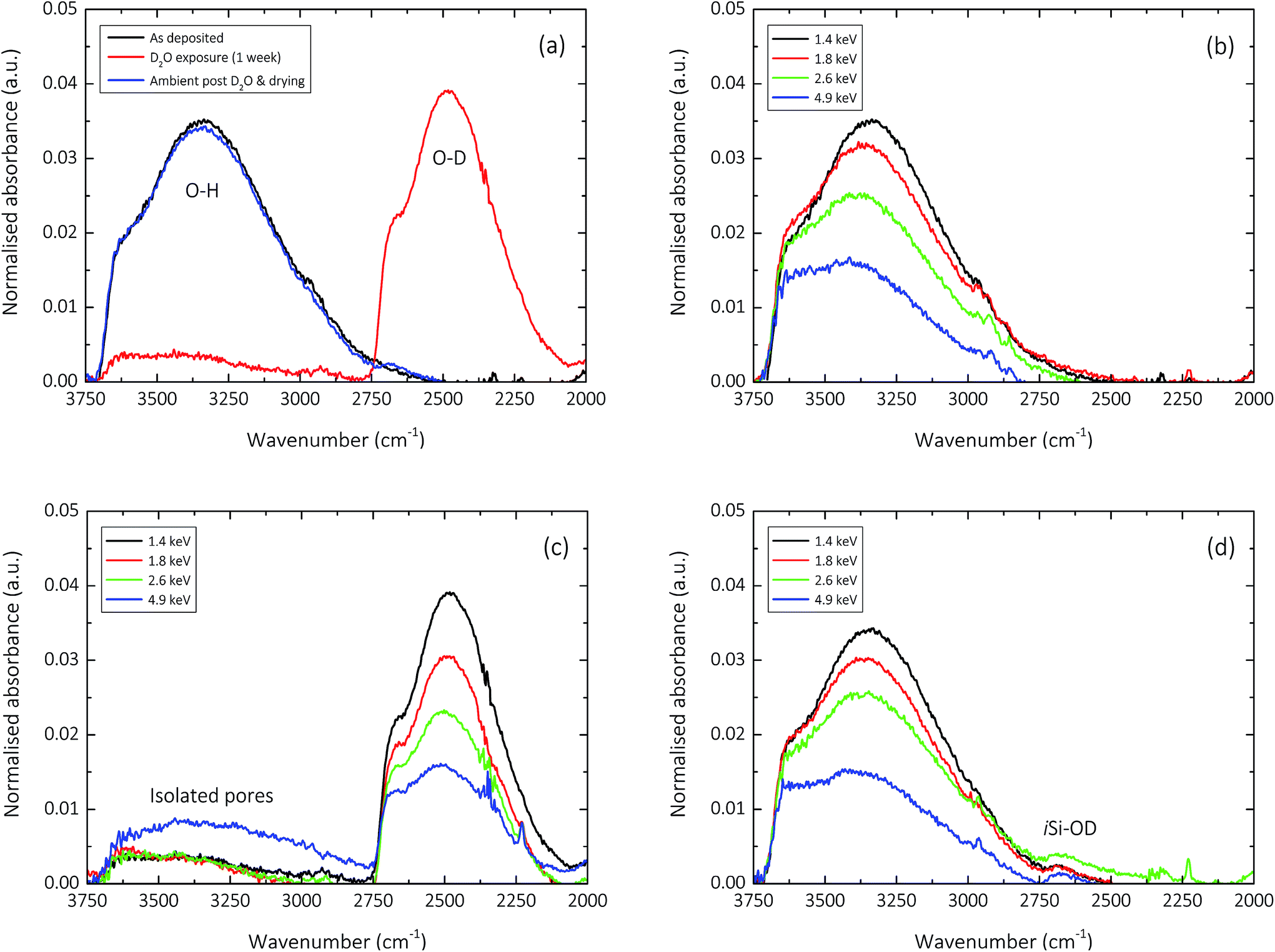 | ||
| Fig. 5 Normalised un-polarized ATR-FTIR absorption spectra showing: (a) the influence of the D2O exposure process upon the hydroxyl (O–H, 3750–3000 cm−1; O–D, 2750–2250 cm−1) stretching region for a 150 nm silica-like thin film deposited with an input E per TEOS of 1.4 keV; the hydroxyl stretching region of 150 nm silica-like thin films deposited with input E per TEOS ranging from 1.4–4.9 keV illustrating films (b) immediately after deposition; (c) after one week exposure to D2O and (d) after one week exposure to ambient air (post D2O contact). | ||
As previously discussed by Elam et al.,12 the hydroxyl groups in the amorphous silica network, whether covalently bonded as in the case of isolated silanol (iSiO–H, 3650 cm−1),53,54,60 and neighbouring silanol (nSiO–H, 3450 cm−1),53,54,64 or unbound in the case of trapped molecular water (HO–H, 3250 cm−1),27,54,64 gradually decrease in concentration with increasing deposition input energy. This characteristic decrease in absorbance can be seen clearly in Fig. 5b. However, what becomes apparent upon exposure to D2O, is the variation in the degree of pore interconnectivity. It appears that samples deposited at specific energies greater than 2.6 keV per TEOS molecule have a greater magnitude of isolated pores within the silica network (Fig. 5c), as the extent of H–D exchange during the one week exposure is significantly less for samples deposited at 4.9 keV per TEOS molecule. This finding directly correlates with the one order of magnitude improvement in encapsulation performance (10−2 to 10−3 g m−2 day−1) observed for films deposited at 4.9 keV per TEOS with respect to 2.6 keV per TEOS (Fig. 2). Upon drying of the samples post D2O exposure and subsequent contact with ambient air for one week, it appears in general that the reverse deuterium–hydrogen exchange occurs, bar a small concentration of deuterium that still remains in all films, covalently bonded in the form of isolated silanol (iSiO–D), as shown in Fig. 5d.
For the purpose of understanding pore interconnectivity in amorphous silica thin films deposited at energies greater than 4.9 keV, the data set was extended to include samples deposited at energies up to 70 keV per TEOS molecule. The results showing the influence of one week exposure to D2O on the hydroxyl stretching region of these films can be seen in Fig. 6.
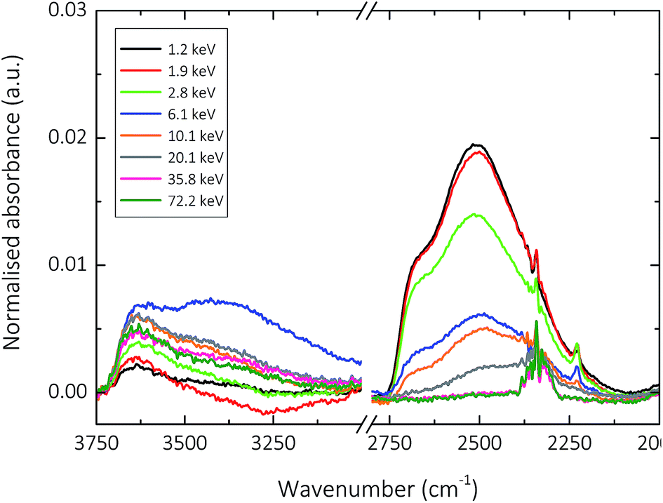 | ||
| Fig. 6 Normalised un-polarized ATR-FTIR absorption spectra showing the influence of one week exposure to D2O upon the hydroxyl (O–H, 3750–3000 cm−1; O–D, 2750–2250 cm−1) stretching region for 200 nm silica-like thin films deposited with input E per TEOS ranging from 1.2–72.2 keV onto a modified PET substrate using AP-PECVD, under conditions replicating those of the barrier layer synthesis. The peaks at ∼2350 cm−1 are due to the carbon dioxide asymmetric stretch. | ||
From the aforementioned polarised ATR-FTIR analysis of these films, it was proposed that a two-part densification process occurs as a function of increasing specific energy during the deposition of amorphous silica films using AP-PECVD. The silica network structure was thought to initially undergo a rapid densification for films synthesised at specific deposition E per TEOS up to ∼6 keV, alongside the steady removal of hydroxyl impurities. This phenomenon can be seen in Fig. 6, with films deposited at energies lower and higher than ∼6 keV displaying different behaviour regarding H–D substitution. Films deposited at specific energies <6 keV show almost complete H–D substitution, suggesting that the silica network is open enough to permit the unhindered permeation of (heavy)water molecules and thus the exchange of hydrogen and deuterium, even for supposedly isolated silanol groups. For films deposited at a specific deposition energy of ∼6 keV however, the pore interconnectivity decreases (the Si–O bond length and Si–O–Si bond angle decreases) to such a degree that only hindered permeation of (heavy)water molecules is permitted, leading merely to partial H–D substitution. This observation holds true for films deposited at energies up to ∼20 keV, after which no H–D substitution is observed. Amorphous silica films deposited at specific energies >20 keV appear to have a network structure impermeable to (heavy)water molecules. The diameter of the pores within the lattice must therefore be <0.265 nm (the kinetic diameter of water), making the few remaining hydroxyl impurities within the silica network of these films completely isolated.
This finding would imply that amorphous silica thin films deposited using AP-PECVD at specific energies greater than 20 keV should show excellent encapsulating ability due to their intrinsically dense nature. However, as mentioned before, the performance of these films can unfortunately be limited by the formation of macro-defects that occur as a result of the gradually intensified processing conditions necessary to achieve such high deposition input energies.12,13
Conclusions
The structure–performance relationships in single layer amorphous silica encapsulation films deposited using industrially scalable and cost-effective roll-to-roll AP-PECVD were evaluated. Extensive polarised ATR-FTIR analysis revealed the intrinsic micro-structure of the amorphous silica rapidly densified as a function of increasing deposition input energy, a parameter that related increasing plasma residence time with decreasing TEOS vapour flow rates. The network densification was confirmed by an increase in the presence of Si–O–Si groups, removal of hydroxyl species, a decrease in Si–O bond length and decrease in Si–O–Si bond angle. In conjunction, exposure of the silica layers to D2O to induce hydrogen–deuterium exchange uncovered a transition in pore interconnectivity as a function of input deposition energy, with a greater magnitude of isolated pores incorporated into silica networks deposited at higher input energies. The technique also permitted the estimation of pore diameters within the lattice structures of the films found to be impermeable to (heavy)water molecules.In addition, the findings exposed a clear correlation between encapsulation performance (WVTR and lag-time) and the intrinsic amorphous microstructure, proving that the intrinsic porosity of AP-PECVD silica films could be controlled merely by varying the deposition precursor flux and plasma residence times. The results presented in this article hereby demonstrate the remarkable potential of AP-PECVD as an economical, reliable and versatile production method for the synthesis of encapsulation films.
Conflicts of interest
There are no conflicts to declare.Acknowledgements
This research received funding from the European Union's Seventh Framework Programme for research, technological development and demonstration under grant agreement number 606889; project ESR7 in the framework of the RAPID (Reactive Atmospheric Plasma processIng – eDucation network) Marie Curie Initial Training Network (http://www.rapid-itn.eu). The work is also in association with the Industrial Partnership Programme i31 (APPFF) that is carried out under an agreement between FUJIFILM Manufacturing Europe B.V. and FOM, which is part of the Netherlands Organisation for Scientific Research (NWO). The author would like to thank Rinie van Beijnen, Emile Gommers, Bruno Korngold and Yieuw-Wing Mok (FUJIFILM Manufacturing Europe B.V., Tilburg, The Netherlands) for their technical assistance.References
- J. Lewis, Mater. Today, 2006, 9, 38–45 CrossRef CAS.
- J.-S. Park, H. Chae, H. K. Chung and S. I. Lee, Semicond. Sci. Technol., 2011, 26, 34001 CrossRef.
- N. Grossiord, J. M. Kroon, R. Andriessen and P. W. M. Blom, Org. Electron., 2012, 13, 432–456 CrossRef CAS.
- Y. C. Han, E. Kim, W. Kim, H.-G. Im, B.-S. Bae and K. C. Choi, Org. Electron., 2013, 14, 1435–1440 CrossRef CAS.
- P. E. Burrows, G. L. Graff, M. E. Gross, P. M. Martin, M. Hall, E. Mast, C. Bonham, W. Bennett, L. Michalski, M. Weaver, J. J. Brown, D. Fogarty and L. S. Sapochak, Proc. SPIE, 2001, 4105, 75–83 CrossRef CAS.
- M. S. Weaver, L. A. Michalski, K. Rajan, M. A. Rothman, J. A. Silvernail, J. J. Brown, P. E. Burrows, G. L. Graff, M. E. Gross, P. M. Martin, M. Hall, E. Mast, C. Bonham, W. Bennett and M. Zumhoff, Appl. Phys. Lett., 2002, 81, 2929–2931 CrossRef CAS.
- G. L. Graff, R. E. Williford and P. E. Burrows, J. Appl. Phys., 2004, 96, 1840–1849 CrossRef CAS.
- S.-W. Seo, E. Jung, C. Lim, H. Chae and S. M. Cho, Thin Solid Films, 2012, 520, 6690–6694 CrossRef CAS.
- A. Morlier, S. Cros, J. P. Garandet and N. Alberola, Sol. Energy Mater. Sol. Cells, 2013, 115, 93–99 CrossRef CAS.
- S. A. Starostin, M. Creatore, J. B. Bouwstra, M. C. M. van de Sanden and H. W. de Vries, Plasma Processes Polym., 2015, 12, 545–554 CrossRef CAS.
- P. A. Premkumar, S. A. Starostin, M. Creatore, H. de Vries, R. M. J. Paffen, P. M. Koenraad and M. C. M. van de Sanden, Plasma Processes Polym., 2010, 7, 635–639 CrossRef CAS.
- F. M. Elam, S. A. Starostin, A. S. Meshkova, B. C. A. M. van der Velden-Schuermans, J. B. Bouwstra, M. C. M. van de Sanden and H. W. de Vries, Plasma Processes Polym., 2017, 14, 1600143 CrossRef.
- F. M. Elam, S. A. Starostin, A. S. Meshkova, B. C. A. M. van der Velden-Schuermans, M. C. M. van de Sanden and H. W. de Vries, J. Phys. D: Appl. Phys., 2017, 50, 25LT01 CrossRef.
- G. Aresta, P. A. Premkumar, S. A. Starostin, H. de Vries, M. C. M. van de Sanden and M. Creatore, Plasma Processes Polym., 2010, 7, 766–774 CrossRef CAS.
- A. S. da Silva Sobrinho, G. Czeremuszkin, M. Latrèche and M. R. Wertheimer, J. Vac. Sci. Technol., A, 2000, 18, 149–157 CAS.
- Y. Leterrier, Prog. Mater. Sci., 2003, 48, 1–55 CrossRef CAS.
- A. P. Roberts, B. M. Henry, A. P. Sutton, C. R. M. Grovenor, G. A. D. Briggs, T. Miyamoto, M. Kano, Y. Tsukahara and M. Yanaka, J. Membr. Sci., 2002, 208, 75–88 CrossRef CAS.
- S. Nagai, J. Appl. Phys., 2013, 114, 174302 CrossRef.
- P. A. Premkumar, S. A. Starostin, H. de Vries, M. Creatore, P. M. Koenraad, W. A. MacDonald and M. C. M. van de Sanden, Plasma Processes Polym., 2012, 9, 1194–1207 CrossRef CAS.
- A. Perrotta, G. Aresta, E. R. J. van Beekum, J. Palmans, P. van de Weijer, M. C. M. van de Sanden, W. M. M. Kessels and M. Creatore, Thin Solid Films, 2015, 595, 251–257 CrossRef CAS.
- A. M. Coclite and K. K. Gleason, J. Appl. Phys., 2012, 111, 73516 CrossRef.
- J. Petersen, J. Bardon, A. Dinia, D. Ruch and N. Gherardi, ACS Appl. Mater. Interfaces, 2012, 4, 5872–5882 CAS.
- W. A. Pliskin, J. Vac. Sci. Technol., 1977, 14, 1064–1081 CrossRef CAS.
- J. Schafer, R. Foest, A. Quade, A. Ohl and K.-D. Weltmann, Plasma Processes Polym., 2009, 6, S519–S524 CrossRef.
- A. Brunet-Bruneau, J. Rivory, B. Rafin, J. Y. Robic and P. Chaton, J. Appl. Phys., 1997, 82, 1330–1335 CrossRef CAS.
- S. C. Deshmukh and E. S. Aydil, Appl. Phys. Lett., 1994, 65, 3185–3187 CrossRef CAS.
- P. Innocenzi, J. Non-Cryst. Solids, 2003, 316, 309–319 CrossRef CAS.
- A. Perrotta, E. R. J. Van Beekum, G. Aresta, A. Jagia, W. Keuning, M. C. M. Van De Sanden, W. M. M. Kessels and M. Creatore, Microporous Mesoporous Mater., 2014, 188, 163–171 CrossRef CAS.
- A. Perrotta, S. J. García, J. J. Michels, A.-M. Andringa and M. Creatore, ACS Appl. Mater. Interfaces, 2015, 7, 15968–15977 CAS.
- A. Perrotta, S. J. García and M. Creatore, Plasma Processes Polym., 2015, 12, 968–979 CrossRef CAS.
- A. Perrotta, W. M. M. Kessels and M. Creatore, ACS Appl. Mater. Interfaces, 2016, 8, 25005–25009 CAS.
- C.-N. Liu, B. Ozkaya, S. Steves, P. Awakowicz and G. Grundmeier, J. Phys. D: Appl. Phys., 2013, 46, 84015 CrossRef.
- S. A. Starostin, S. Welzel, Y. Liu, B. van der Velden-Schuermans, J. B. Bouwstra, M. C. M. van de Sanden and H. W. de Vries, Eur. Phys. J.: Appl. Phys., 2015, 71, 20803 CrossRef.
- A. S. Meshkova, Y. Liu, F. M. Elam, S. A. Starostin, M. C. M. van de Sanden and H. W. de Vries, Plasma Processes Polym., 2017, e1700093 CrossRef.
- N. J. Harrick, J. Phys. Chem., 1960, 64, 1110–1114 CrossRef CAS.
- W. A. Pliskin and H. S. Lehman, J. Electrochem. Soc., 1965, 112, 1013–1019 CrossRef CAS.
- N. Rochat, A. Chabli, F. Bertin, M. Olivier, C. Vergnaud and P. Mur, J. Appl. Phys., 2002, 91, 5029–5034 CrossRef CAS.
- G. Laroche, J. Fitremann and N. Gherardi, Appl. Surf. Sci., 2013, 273, 632–637 CrossRef CAS.
- W. Bensch and W. Bergholz, Semicond. Sci. Technol., 1990, 5, 421–428 CrossRef CAS.
- C. Martinet and R. A. B. Devine, J. Non-Cryst. Solids, 1995, 187, 96–100 CrossRef CAS.
- M. K. Gunde, Phys. B, 2000, 292, 286–295 CrossRef CAS.
- M. C. Payne and J. C. Inkson, J. Non-Cryst. Solids, 1984, 68, 351–360 CrossRef CAS.
- S. W. de Leeuw and M. F. Thorpe, Phys. Rev. Lett., 1985, 55, 2879–2882 CrossRef CAS PubMed.
- F. L. Galeener and G. Lucovsky, Phys. Rev. Lett., 1976, 37, 1474–1477 CrossRef CAS.
- A. Parikh and D. Allara, J. Chem. Phys., 1992, 96, 927–945 CrossRef CAS.
- R. M. Almeida, Phys. Rev. B: Condens. Matter Mater. Phys., 1992, 45, 161–170 CrossRef CAS.
- D. W. Berreman, Phys. Rev., 1963, 130, 2193–2198 CrossRef CAS.
- T. Hirata, J. Phys. Chem. Solids, 1997, 58, 1497–1501 CrossRef CAS.
- G. Lucovsky, C. K. Wong and W. B. Pollard, J. Non-Cryst. Solids, 1983, 59–60, 839–846 CrossRef CAS.
- P. G. Pai, S. S. Chao, Y. Takagi and G. Lucovsky, J. Vac. Sci. Technol., A, 1986, 4, 689–694 CAS.
- C. T. Kirk, Phys. Rev. B: Condens. Matter Mater. Phys., 1988, 38, 1255–1273 CrossRef CAS.
- C. Vallee, A. Goullet, A. Granier, A. van der Lee, J. Durand and C. Marliere, J. Non-Cryst. Solids, 2000, 272, 163–173 CrossRef CAS.
- M. Creatore, J.-C. Cigal, G. M. W. Kroesen and M. C. M. van de Sanden, Thin Solid Films, 2005, 484, 104–112 CrossRef CAS.
- M. Creatore, S. M. Rieter, Y. Barrell, M. C. M. van de Sanden, R. Vernhes and L. Martinu, Thin Solid Films, 2008, 516, 8547–8553 CrossRef CAS.
- P. Lange, J. Appl. Phys., 1989, 66, 201–204 CrossRef CAS.
- J. S. Chou and S. C. Lee, J. Appl. Phys., 1995, 77, 1805–1807 CrossRef CAS.
- M. Nakamura, Y. Mochizuki, K. Usami, Y. Itoh and T. Nozaki, J. Electrochem. Soc., 1985, 132, 482–488 CrossRef CAS.
- E. Hensel, K. Wollschlager, D. Schulze, U. Kreissig, W. Skorupa and J. Finster, Surf. Interface Anal., 1985, 7, 207–210 CrossRef CAS.
- I. W. Boyd and J. I. B. Wilson, Appl. Phys. Lett., 1987, 50, 320–322 CrossRef CAS.
- J. A. Theil, D. V Tsu, M. W. Watkins, S. S. Kim and G. Lucovsky, J. Vac. Sci. Technol., A, 1990, 8, 1374–1381 CAS.
- T. M. Parrill, J. Mater. Res., 1994, 9, 723–730 CrossRef CAS.
- R. A. B. Devine, J. Vac. Sci. Technol., A, 1988, 6, 3154–3156 CAS.
- J. Coates, in Encyclopedia of Analytical Chemistry, ed. R. A. Meyers, John Wiley & Sons Ltd, Chichester, 2000, pp. 10815–10837 Search PubMed.
- L. B. Capeletti, I. M. Baibich, I. S. Butler and J. H. Z. dos Santos, Spectrochim. Acta, Part A, 2014, 133, 619–625 CrossRef CAS PubMed.
| This journal is © The Royal Society of Chemistry 2017 |