
 Open Access Article
 This Open Access Article is licensed under a Creative Commons Attribution-Non Commercial 3.0 Unported Licence
A silver nanowire mesh overcoated protection layer with graphene oxide as a transparent electrode for flexible organic solar cells†
Byung-Yong Wanga,
Eung-Seok Leea,
Young-Jei Oh*b and
Hyun Wook Kang *c
*c
aCenter for Semiconductor Technology, Korea University, 145 Anam-ro, Seongbuk-gu, Seoul, 02841, Republic of Korea
bOpto Electronic Materials and Devices Center, Korea Institute of Science and Technology, 5 Hwarang-ro 14-gil, Seongbuk-gu, Seoul 02792, Republic of Korea
cDepartment of Mechanical Engineering, Chonnam National University, 77 Yongbong-ro, Buk-gu, Gwangju 61186, Republic of Korea. E-mail: kanghw@chonnam.ac.kr; Tel: +82-62-530-1662
First published on 15th November 2017
Abstract
For high-throughput flexible electronic devices to be ready for the market, their transparent conductive electrodes (TCEs) should show stable working performance during folding conditions and have a long operating life. In this study, TCEs were produced by over-coating silver nanowire (AgNW) electrodes with graphene oxide (GO). The GO/AgNW electrodes showed an outstanding sheet resistance value of 18 Ω−1, 87% transmittance, mechanical stability, and excellent long-term stability. Furthermore, the GO film wrapped around the AgNWs, which improved the inter-nanowire junction resistance and lowered the surface roughness without any heat treatments or high-force pressing processes. Flexible P3HT:PC60BM- and PTB7:PC70BM-based organic solar cells (OSCs) were produced using the GO/AgNW transparent electrodes on a flexible polyethylene terephthalate substrate. The GO/AgNW electrode exhibited a higher optical absorption in all the OSCs compared to those of the indium tin oxide (ITO) electrodes and showed a high short circuit current of 3 mA cm−2. Consequently, the fabricated OSCs showed a 7% higher efficiency than the ITO electrodes. In addition, after 50 bending tests, the efficiency of the GO/AgNW electrodes changed less than 3%. Thus, the GO/AgNW electrodes showed enhanced results in terms of resistance and durability compared to conventional transparent electrodes, including ITO-based electrodes.
1. Introduction
Organic solar cells (OSCs) offer a simple device structure, and they can be produced on a large scale by roll-to-roll processing on polymer substrates. As the interest in flexible solar cells increases, so does the demand for lightweight OSCs that can be freely bent or folded like paper. Moreover, the use of such flexible OSCs will allow design of devices that can be freely changed and will enable such devices to be fabricated for a curved surface and to be rolled like a roll of paper. Thus, OSCs can be used in various applications, including wearable electronic devices.1–6 However, transparent electrodes with high conductivity and flexibility must be developed for OSCs to be flexible.Currently, indium tin oxide (ITO) is widely used as a transparent electrode material due to its high electrical conductivity, excellent chemical stability, and high light transmittance, but it is limited as a next-generation electrode because of its high price and inadequate indium resources. Another disadvantage of ITO film is its brittleness, which makes coating it onto a flexible plastic substrate difficult. Furthermore, it absorbs in the UV/blue region, which is a drawback when applied to solar cells. These problems motivate the development of new types of transparent conductive electrodes (TCEs). Conducting polymers, carbon nanotubes, graphene, and metal networks have all been investigated as alternatives to ITO.7–15
In the case of organic conducting polymers, electrical conductivity increases proportionally with electrode thickness. However, a thick electrode layer comes at the cost of decreased transmittance because conducting polymers absorb light in the visible region; thus, electrode films must be thinly coated (100 nm or less) with such polymers. Reaching a sheet resistance of 80 Ω−1 is difficult with a 100 nm-thick coating.16–18 Another candidate for transparent electrodes is carbon nanotubes (CNTs), which exhibit excellent electrical conductivity and high transmittance, and achieving a low sheet resistance (10 Ω−1) requires a large quantity of CNTs. Thus, the electrode becomes black while maintaining transparency results in decreased transmittance. In the case of transparent graphene electrodes, the defective bond between the graphene flakes and the current collector leads to high contact resistance and thus high sheet resistance.19,20
To overcome these problems, silver nanowires (AgNWs) are arising as a next-generation material because they exhibit excellent electrical and optical characteristics, and they are easy to manufacture on a large scale and at a low cost through a solution process. In addition, flexibility can be easily achieved due to their long, thin morphology.21–28
However, this material is not free of problems. The biggest challenge is that AgNWs are oxidized by oxygen, which lowers the electrical conductivity and transparency. Another problem is that AgNW coatings easily separate from their substrate due to a low adhesive force.24,29–32 Furthermore, when AgNWs are applied to the transparent electrode of solar cells, the high surface roughness of the AgNWs causes a low shunt resistance, high dark current, and low efficiency.33 Thus, using AgNWs to fabricate high-efficiency optoelectronic devices has many drawbacks. To address these issues, innovative techniques have recently been reported for improving the adhesive force while lowering the surface roughness by adapting an over-coating layer (OCL) and protecting layer for the AgNWs using conducting polymers and oxides, such as zinc oxide (ZnO). These methods, however, require a thick coating as a top-coat material (conducting polymers, oxides, etc.) to lower the inherent surface roughness of the AgNWs, which also lowers the optical transmittance.
Therefore, in this report, a very thin graphene oxide (GO) layer whose transparency is not low was formed via spray coating to preventing the AgNW transparent electrode from oxidizing in air. The GO dispersion was hydrophilic due to its oxygen functional groups but was not electrically conductive.34–36 As a result, a transparent electrode could be fabricated with low surface roughness and a high adhesive force, which featured a thin GO layer that could directly pass currents via tunneling, even though it is an insulator, thereby improving the electrical characteristics of the AgNWs.33 Significantly, the AgNWs did not oxidize, even when exposed to the air for over two months. Furthermore, a flexible OSC was produced using a GO/AgNW transparent electrode on a polyethylene terephthalate (PET) substrate.37–39
2. Experiments
2.1 Preparation of a GO/AgNWs TCE
In this study, an ink was prepared with highly linear AgNWs with a thickness of 40 nm and a length of 45 μm, which had been fabricated in a previous experiment. The ink was slot-die coated using a slot-die coater on a PET substrate. For the OCL, the GO (Angstron Materials) with an X–Y dimension of 1 μm or less and a thickness of 1–1.2 nm was used. First, 1 mg of GO was diluted in 10 mL of DI water, and a spray coater was used to prepare the coating. To remove the solvent, the substrate was heated to 110 °C during the experiment. The fabricated GO/AgNW transparent conductive film showed 87% light transmittance and a sheet resistance of 18 Ω−1, which is similar to the 90% light transmittance and 12 Ω−1 sheet resistance of commercial ITO (JMC, South Korea) (Fig. 1). Even though GO is an insulator, if it is coated very thinly on the AgNWs, electrons can easily move through it by ohmic contact and direct tunneling (Fig. S1†). Furthermore, the GO that was used in this experiment had characteristic G- and D-band peaks at 1611 and 1356 cm−1, respectively, as shown in Fig. S2.† These peaks in the G- and D-bands grow as the amount of GO increases. Hence, the presence of GO can be verified in the OCL. | ||
| Fig. 1 Total transmittance spectra of ITO- and GO/AgNW-coated films. | ||
2.2 Fabrication of organic solar cells
OSCs were fabricated using the transparent GO/AgNW electrode. A poly-3,4-ethylenedioxythiophene–polystyrenesulfonate (PEDOT:PSS) bilayer (CleviosTM PH 1000 and P VP AI 4083, respectively) was spin-coated to a 100 nm thickness as a hole transport layer (HTL) on the GO/AgNW substrate. The PEDOT:PSS was mixed with methanol (Aldrich) at a 1![[thin space (1/6-em)]](https://www.rsc.org/images/entities/char_2009.gif) :1 volume ratio, and this solution was spin-coated at 4000 rpm for 40 s and annealed at 130 °C for 30 min in a glove box. Then, 18 mg of P3HT (Rieke Metals, Inc.) and 10.8 mg of PC60BM were melted in 1 mL of chlorobenzene as an electron transport layer (ETL). The mixture was spun at 2500 rpm for 40 s and was thermally treated in a glove box at 150 °C for 10 min. In addition, OSCs with high power conversion efficiencies (PCEs) were fabricated using poly[4,8-bis[(2-ethylhexyl)oxy]benzo[1,2-b:4,5-bA]dithiophene-2,6-diyl][3-fluoro-2-[(2-ethylhexyl)carbonyl]thieno[3,4-b]-thiophenediyl] (PTB7) and [6,6]-phenyl-C71-butyric acid methyl ester (PC70BM), which are low-bandgap polymers. The fabrication method was identical to that of the P3HT:PC60BM system. PTB7:PC70BM (1-materials) was dissolved at a 1:1.5 weight ratio in chlorobenzene:1,8-diiodoctane (97:3) before being spun at 1000 rpm for 40 s and then annealed at 50 °C for 10 min in a glove box.
:1 volume ratio, and this solution was spin-coated at 4000 rpm for 40 s and annealed at 130 °C for 30 min in a glove box. Then, 18 mg of P3HT (Rieke Metals, Inc.) and 10.8 mg of PC60BM were melted in 1 mL of chlorobenzene as an electron transport layer (ETL). The mixture was spun at 2500 rpm for 40 s and was thermally treated in a glove box at 150 °C for 10 min. In addition, OSCs with high power conversion efficiencies (PCEs) were fabricated using poly[4,8-bis[(2-ethylhexyl)oxy]benzo[1,2-b:4,5-bA]dithiophene-2,6-diyl][3-fluoro-2-[(2-ethylhexyl)carbonyl]thieno[3,4-b]-thiophenediyl] (PTB7) and [6,6]-phenyl-C71-butyric acid methyl ester (PC70BM), which are low-bandgap polymers. The fabrication method was identical to that of the P3HT:PC60BM system. PTB7:PC70BM (1-materials) was dissolved at a 1:1.5 weight ratio in chlorobenzene:1,8-diiodoctane (97:3) before being spun at 1000 rpm for 40 s and then annealed at 50 °C for 10 min in a glove box.
Finally, the LiF/Al electron-collecting top electrode was subjected to thermal evaporation to produce the final OSCs, and the thickness of each layer was observed by transmission electron microscopy (TEM) (Fig. 2). A control OSC was fabricated with an ITO/glass electrode as a reference for comparison, and all the processes were carried out identically.
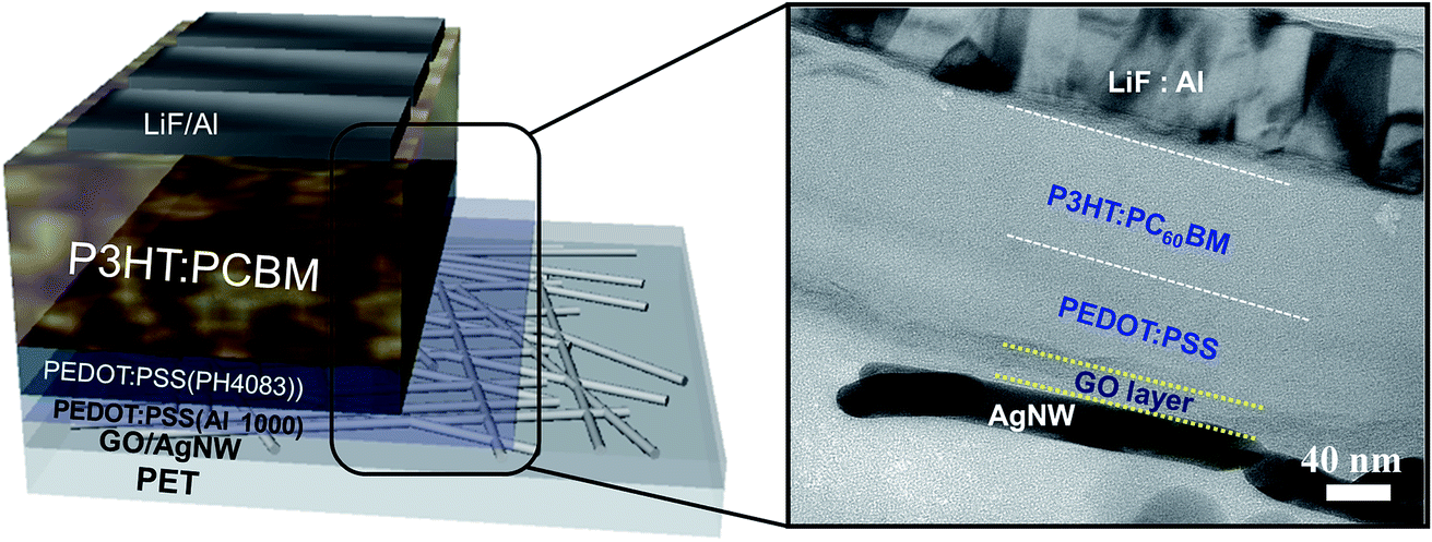 | ||
| Fig. 2 A schematic cross-sectional view of P3HT:PC60BM-based OSCs with GO/AgNW and the corresponding cross-sectional high-resolution transmission electron microscopy (HRTEM) image. | ||
2.3 Material and device characterization
The sheet resistance of the GO/AgNW transparent electrode was measured with a Keithley 2400 source meter by a 4-point probe method, and the transmittance was analyzed by an ultraviolet-visible spectroscopy (Perkin Elmer UV/Vis spectrometer Lamda 18). The GO structure was analyzed using Raman spectrometry. The haze factor of the GO/AgNW film was measured with a commercial haze spectrometer (Sinco). The surface of the transparent electrode was analyzed with a scanning electron microscope (SEM; XL-30 EDAX, Philips, Netherlands) and an atomic force microscope (AFM; Digital Instruments Dimension 3100, equipped with a Nanoscope IV controller). To evaluate the flexibility of the transparent electrode, the GO/AgNW/PET and ITO/PET transparent electrodes were compared using a bending test machine (ZB-100, Z-Tech) at a radius of 10 mm for 10000 cycles.
The performance of the OSCs fabricated with the GO/AgNW transparent electrodes was analyzed using an ORIEL solar simulator with a 150 W light source. To achieve the AM 1.5 condition and 100 mW cm−2 intensity, the intensity of the reference light source was calibrated using a standard Si photodiode. The external quantum efficiency (EQE) was measured using an ORIEL IQE 200 system. In addition, a cross-section of the OSCs was observed with a transmission electron microscope (TEM; JEM 2100F) using a focused ion beam (FIB) milling technique.
2.4 FDTD simulation methods
To compare the light-scattering characteristics of the AgNWs, a commercial finite difference time domain (FDTD) simulation tool (Lumerical Solution, Inc.) was used. For the simulation mesh, a uniform size of 0.25 nm was used for all the directions. Furthermore, a 300–800 nm wavelength light source was used. To evaluate the characteristics of the laminated-structure OSCs, the thickness of each layer was set to be identical to the corresponding thickness in the actual device.3. Results and discussion
The AgNWs were fabricated by the reported polyol method,40 which is a simple method of synthesizing AgNWs by growing reduced Ag ions in the [111] direction using a capping agent. The crystal structure of the synthesized AgNWs was analyzed via X-ray diffraction (XRD), which showed (111), (200), and (220) crystalline peaks, indicating a face-centered cubic structure (JCPDS Card no. 89-3722), as shown in Fig. S3.† Furthermore, the AgNWs grew with a pentagonal cross-section, and the synthesized AgNWs had a diameter of 45 nm and a minimum length of 40 μm (Fig. 3).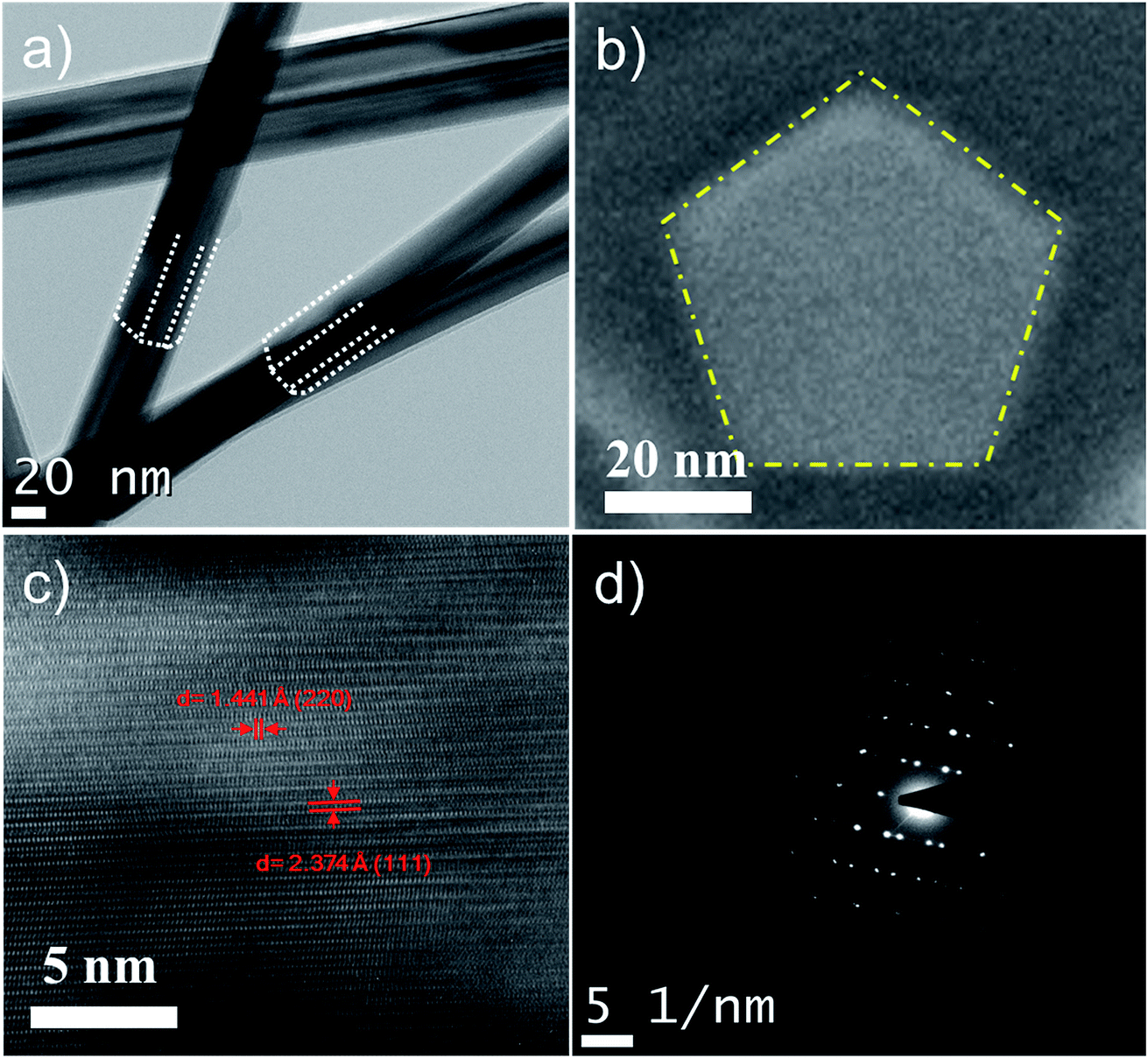 | ||
| Fig. 3 Transmission electron microscope (TEM) images of (a) AgNWs (b) a AgNW cross-section. (c) Lattice fringes and (d) selected area electron diffraction (SAED) pattern of the AgNWs. | ||
The AgNWs are thin and long and thus are easily oxidized because their surface-to-volume ratio is much greater than that of the bulk material. For this reason, when the AgNWs are exposed to the air without a protective layer, they quickly oxidize or corrode. Fig. 4 shows SEM results for the stability the AgNWs in air. As described above, when the AgNWs were coated with GO as a protective layer, the AgNWs showed no change even after two weeks. In contrast, when the AgNWs were used without a protective coating, they generally oxidized and corroded. Furthermore, the high acidity and sulfur molecules of the conducting polymer PEDOT:PSS can both damage the AgNWs, which makes using this material as a transparent electrode for a long time difficult. However, when the long-term stability was tested, the AgNW with the GO protective layer showed excellent stability with no changes in resistance for two months in air. However, when the AgNWs were used without the protective layer, the electrode's resistance sharply increased after 10 days. When PEDOT:PSS was used as a protective layer, the resistance sharply increased after 3 days at rest. These increases in the resistance were due to oxidization and corrosion, as explained above. The AgNWs with the GO protective layer showed excellent long-term chemical stability, even after long-term exposure to air (Fig. 5).
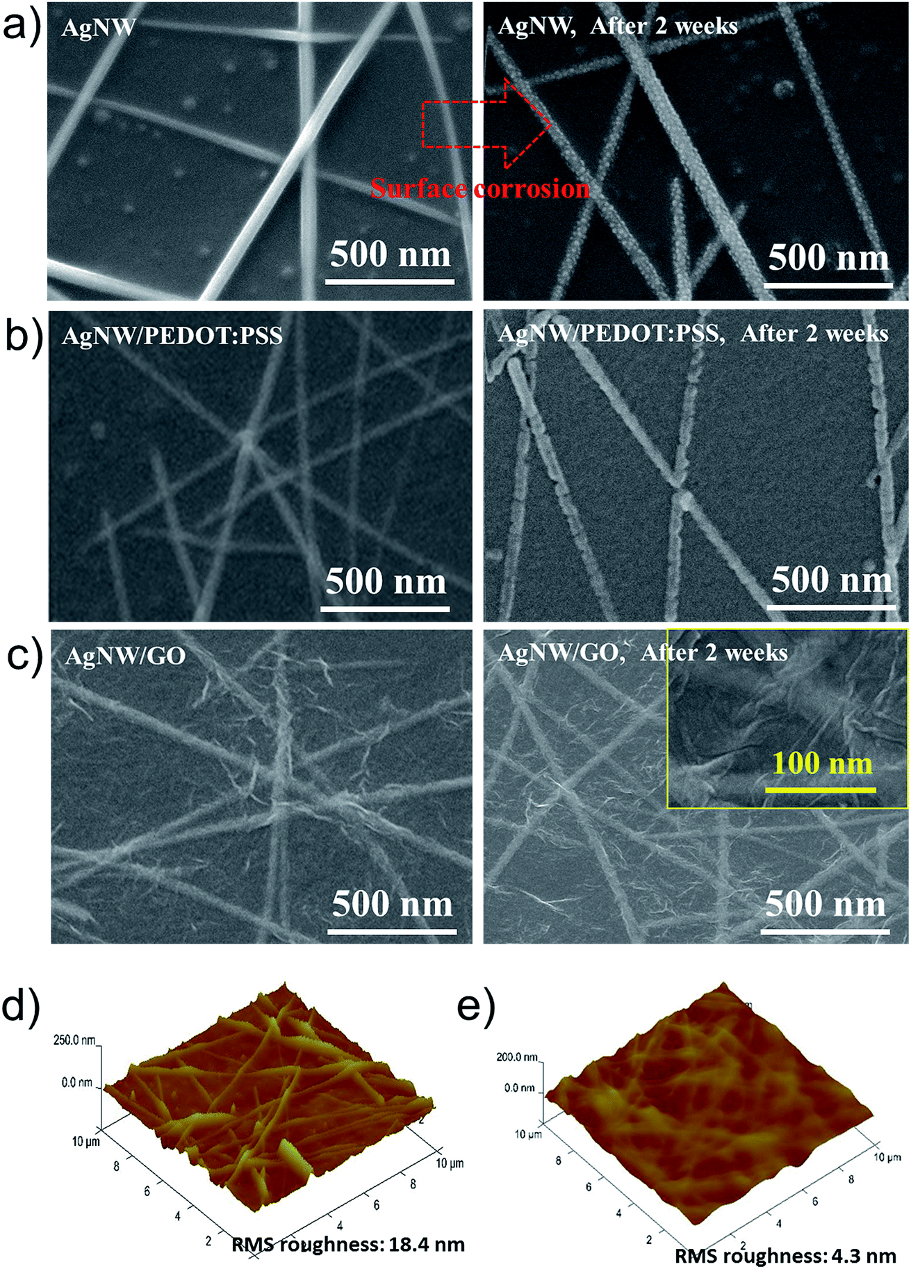 | ||
| Fig. 4 SEM images of (a) AgNWs and the (b) PEDOT:PSS/AgNW and (c) GO/AgNW hybrid transparent electrodes after a long-term stability test at room temperature for 2 weeks. Atomic force microscopy (AFM) images of AgNWs on PET (d) with and (e) GO/AgNW electrodes. | ||
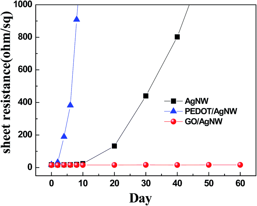 | ||
| Fig. 5 Plot of the mean Rsh versus time for the AgNW/PET, PEDOT:PSS/AgNW/PET and GO/AgNW/PET films exposed to air up to 2 months. | ||
As mentioned above, fabricating highly efficient optoelectronic devices, such as OSCs with AgNWs, is difficult due to the shunt resistance, high dark current, and low efficiency resulting from the high surface roughness of AgNWs.32 When the roughness of a transparent electroconductive film coated with AgNWs alone was compared to that of the GO/AgNW electroconductive film (Fig. 4d and e), the former showed a high surface roughness of 46.8 nm due to the presence of the AgNWs and the empty spaces between them, whereas the latter showed a low surface roughness of 4.3 nm. The reason for the low surface roughness is that the empty spaces are filled with GO, as shown in the SEM image, which offsets the high roughness of the AgNWs.
Furthermore, the GO/AgNW transparent electroconductive film showed excellent flexibility. The bending test demonstrated that due to the brittleness of ITO film, it cracked when the bending radius decreased, and the resistance sharply increased to at least 70% higher than the initial resistance. In contrast, for the GO/AgNW transparent electrode, the GO prevented the AgNWs from separating and losing contact with each other, and a small change in resistance of under 2% was observed, even after 10000 cycles, indicating superior mechanical stability to that of the ITO transparent electrode (Fig. 6).
 | ||
| Fig. 6 Variation in the resistance of the GO/AgNW film as a function of the number of bending cycles. | ||
Fig. 7a and b and Table 1 show the results of the OSCs fabrication to verify the possibility of adapting the GO/AgNW transparent electrode as a flexible optoelectronic device. The commercial ITO on glass with 90% transmittance and a 12 Ω−1 sheet resistance was compared with the GO/AgNW/PET transparent electrode with 87% transmittance and an 18 Ω−1 sheet resistance. In the case of the P3HT:PCBM system, the ITO electrode showed an open-circuit voltage (Voc) of 0.62 ± 0.00 V, a short-circuit current (Jsc) of 7.97 ± 0.27 mA cm−2, a fill factor (FF) of 0.63 ± 0.02, and a PCE of 3.18 ± 0.04% (highest: 3.27). The GO/AgNW electrode showed a Voc of 0.60 ± 0.00 V, a Jsc of 9.17 ± 0.41 mA cm−2, an FF of 0.59 ± 0.00, and a PCE of 3.25 ± 0.08% (highest: 3.32). The Jsc of the GO/AgNW electrode was higher than that of the conventional ITO transparent electrode (Fig. 7a). In the PTB7:PC70BM-based system, the GO/AgNW electrode showed a Voc of 0.68 ± 0.00 V, a Jsc of 19.84 ± 0.57 mA cm−2, an FF of 0.57 ± 0.01, and a PCE of 7.62 ± 0.10% (highest: 7.66), and its Jsc was higher than that of the ITO electrode (Fig. 7b). All three GO/AgNW electrodes showed the same trends. The details of the average performance parameter values of Voc, Jsc, FF, and PCE for all the devices are summarized in Table 1. All OSC performance metrics were averaged from the results of four devices.
 | ||
| Fig. 7 Representative J–V characteristics of P3HT:PC60BM and PTB7:PC70BM OSCs with the GO/AgNW mesh electrode and the reference device with the ITO electrode under AM 1.5 G illumination with 100 mW cm−2 intensity. (a) P3HT:PC60BM, (b) PTB7:PC70BM. (c) Magnified diffuse transmittance spectra of ITO and GO/AgNW films and (d) simulated light absorption maps in the devices with ITO and GO/AgNW. | ||
| Voc (mV) | Jsc (mA cm−2) | FF | PCE (%) | |
|---|---|---|---|---|
| a Values from 3 and 4 devices were averaged, and the PCEs in parentheses indicate the highest values. | ||||
| P3HT:PC60BM ITO (batch 1) | 0.62 ± 0.00 | 7.97 ± 0.27 | 0.63 ± 0.02 | 3.18 ± 0.04 (3.27) |
| P3HT:PC60BM GO/AgNW (batch 1) | 0.60 ± 0.00 | 9.17 ± 0.41 | 0.59 ± 0.00 | 3.25 ± 0.08 (3.32) |
| P3HT:PC60BM GO/AgNW (batch 2) | 0.59 ± 0.01 | 9.53 ± 0.17 | 0.57 ± 0.01 | 3.26 ± 0.05 (3.31) |
| PTB7:PC70BM ITO (batch 1) | 0.74 ± 0.00 | 16.32 ± 0.03 | 0.58 ± 0.01 | 7.14 ± 0.10 (7.27) |
| PTB7:PC70BM GO/AgNW (batch 1) | 0.67 ± 0.01 | 19.79 ± 0.01 | 0.55 ± 0.01 | 7.32 ± 0.06 (7.38) |
| PTB7:PC70BM GO/AgNW (batch 2) | 0.69 ± 0.00 | 18.15 ± 0.01 | 0.59 ± 0.01 | 7.53 ± 0.02 (7.56) |
| PTB7:PC70BM GO/AgNW (batch 3) | 0.68 ± 0.00 | 19.84 ± 0.57 | 0.57 ± 0.01 | 7.62 ± 0.10 (7.66) |
The Voc of OSCs is influenced by the sheet resistance and energy bandgap, and the Jsc is influenced by the transmittance. The higher the transmittance, the greater the light absorption becomes, which increases the Jsc. As shown in Fig. 7a and b and Table 1, the GO/AgNW electrode showed a low Voc value in all the devices because its sheet resistance was higher by at least 6 Ω−1 than that of the ITO electrode. The GO/AgNW electrode, however, showed an approximately 3 mA cm−2 higher Jsc, even though its transmittance was lower by at least 3% than that of the ITO electrode.
The reason for this higher Jsc is the effect of the optical properties. As shown in Fig. 1, the spectra are similar to one another in the visible region, but the transmittance of GO/AgNW is higher in the 300–400 nm range and at 600 nm. As a result, more external photons are absorbed into the working layer of the device, which increases the phototransformation efficiency. In fact, measurements of the external quantum efficiency (EQE) indicate that higher phototransformation efficiency appears near 400 and 600 nm (Fig. S4†). Furthermore, the haze measurements show that the GO/AgNW has higher light scattering than ITO (Fig. 7c). This higher light scattering can be interpreted as a photon trapping effect, in which the photons discharged from the working layer that do not react with the photoactive material are reflected from the GO/AgNW layer and are returned to the working layer. The FDTD simulation result showed that the working layer absorbed more light, as shown in Fig. 7d. As described above, the efficiency of the OSCs increased as a result of the increase in the Jsc due to the increased light absorption, despite the low transmittance. Fig. 8 shows the changes in the efficiency of the fabricated OSCs before and after 50 bending cycles. The OSCs using the GO/AgNW electrode showed a small change in efficiency of below 3%. As with the previous bending test results, the GO/AgNW electrode maintained its electrical path even after many bending cycles due to its excellent mechanical stability, and the efficiency of the OSCs did not change appreciably.
 | ||
| Fig. 8 Photographs of the continuous mechanical bending experiment of a P3HT:PC60BM OSC with the GO/AgNW mesh and selected J–V characteristics during bending cycles up to 50. | ||
4. Conclusion
AgNWs were used as an electrode material on flexible substrates to replace the conventional ITO electrode. A flexible PET substrate was slot-die coated with the AgNWs, and the AgNWs were spray-coated with GO over-coatings to produce a new transparent electrode with enhanced stability that showed excellent characteristics of 87% transmittance and 18 Ω−1 sheet resistance. The fabricated transparent electrode showed high long-term stability and improved durability due to introducing the GO OCL, which lowered the inherently high surface roughness of the AgNW transparent electrode that had previously created a problem when the AgNW transparent electrode was applied to the OSCs. Furthermore, the fabricated GO/AgNW electrode OSCs showed higher efficiency than the OSCs with the conventional ITO transparent electrode because it absorbed more light in the working layer, and the GO/AgNW OSCs exhibited Jsc values of 9.17 ± 0.41 mA cm−2 for P3HT:PC60BM and 19.84 ± 0.57 mA cm−2 for PTB7:PC70BM. This resulted in enhanced PCEs of 3.32 and 7.66% due to the light transmittance characteristics of the GO/AgNW electrodes near 300–400 and 600 nm as well as the light scattering and trapping effects, even though the GO/AgNW transparent electrode had a sheet resistance higher by at least 6 Ω−1 and a transmittance lower by at least 3% than those of the ITO electrode. This improved light absorption correlated with the light transmittance and scattering, which was verified by measuring the haze factor and by a FDTD simulation. In addition to the improved device performance, the OSCs fabricated using the GO/AgNW electrodes showed a negligible change in efficiency (lower than 3%) after being subjected to 50 bending cycles. Furthermore, the developed GO/AgNW transparent electrode allows for devices with a large area, low cost, and high flexibility. Therefore, this electrode can be used to produce next generation flexible OSCs applicable to the outer walls of buildings and curved surfaces, which will cause great changes to the solar cell market. Moreover, due to their low surface roughness and excellent electrical and optical characteristics, the GO/AgNW electrodes are expected to be applicable to various flexible electronic devices, including low-cost OSCs, organic light-emitting diode (OLED), organic memory and organic transistor devices.41–43Conflicts of interest
There are no conflicts to declare.Acknowledgements
B.-Y. W. and E.-S. L. contributed equally to this work. The authors would like to acknowledge the financial support from the Basic Science Research Program through the National Research Foundation of Korea (NRF) funded by the Ministry of Science, ICT & Future Planning (2016R1C1B2012136).References
- H. Y. Chen, J. H. Hou, S. Q. Zhang, Y. Y. Liang, G. W. Yang, Y. Yang, Y. Luping, W. Yue and L. Gang, Polymer Solar Cells with Enhanced Open-circuit Voltage and Efficiency, Nat. Photonics, 2009, 3, 649–653 CrossRef CAS.
- H. X. Zhou, L. Q. Yang, A. C. Stuart, S. C. Price, S. B. Liu and W. You, Development of Fluorinated Benzothiadiazole as a Structural Unit for a Polymer Solar Cell of 7% Efficiency, Angew. Chem., Int. Ed., 2011, 50, 2995–2998 CrossRef CAS PubMed.
- Z. C. He, C. M. Zhong, S. J. Su, M. Xu, H. B. Wu and Y. Cao, Enhanced Power-Conversion Efficiency in Polymer Solar Cells Using an Inverted Device Structure, Nat. Photonics, 2012, 6, 591–595 Search PubMed.
- C. E. Small, S. Chen, J. Subbiah, C. M. Amb, S. W. Tsang, T. H. Lai, J. R. Reynolds and F. So, High-Efficiency Inverted Dithienogermole-Thienopyrrolodione-Based Polymer Solar Cells, Nat. Photonics, 2012, 6, 115–120 CrossRef CAS.
- S. H. Liao, H. J. Jhuo, Y. S. Cheng and S. A. Chen, Fullerene Derivative-Doped Zinc Oxide Nanofilm as the Cathode of Inverted Polymer Solar Cells with Low-Bandgap Polymer (PTB7-Th) for High Performance, Adv. Mater., 2013, 25, 4766–4771 CrossRef CAS PubMed.
- D. S. Ginley, Handbook of Transparent Conductors, Springer, New York, 2010 Search PubMed.
- B. Zhang, X. P. Dong, X. F. Xu, X. J. Wang and J. S. Wu, Electrical and Optical Properties of ITO and ITO : Zr Transparent Conducting Films, Mater. Sci. Semicond. Process., 2007, 10, 264–269 CrossRef CAS.
- T. Durkop, S. A. Getty, E. Cobas and M. S. Fuhrer, Extraordinary Mobility in Semiconducting Carbon Nanotubes, Nano Lett., 2004, 4, 35–39 CrossRef.
- N. Manavizadeh, F. A. Boroumand, E. Asl-Soleimani, F. Raissi, S. Bagherzadeh, A. Khodayari and M. A. Rasouli, Influence of Substrates on the Structural and Morphological Properties of RF Sputtered ITO Thin Films for Photovoltaic Application, Thin Solid Films, 2009, 517, 2324–2327 CrossRef CAS.
- D. Kim, L. Zhu, D. J. Jeong, K. Chun, Y. Y. Bang, S. R. Kim, J. H. Kim and S. H. Oh, Transparent Flexible Heater Based on Hybrid of Carbon Nanotubes and Silver Nanowires, Carbon, 2013, 63, 530–536 CrossRef CAS.
- D. S. Hecht, L. B. Hu and G. Irvin, Emerging Transparent Electrodes Based on Thin Films of Carbon Nanotubes, Graphene, and Metallic Nanostructures, Adv. Mater., 2011, 23, 1482–1513 CrossRef CAS PubMed.
- M. Song, D. S. You, K. Lim, S. Park, S. Jung, C. S. Kim, D. H. Kim, D. G. Kim, J. K. Kim, J. Park, Y. C. Kang, J. Heo, S. H. Jin, J. H. Park and J. W. Kang, Highly Efficient and Bendable Organic, Solar Cells with Solution-Processed Silver Nanowire Electrodes, Adv. Funct. Mater., 2013, 23, 4177–4184 CrossRef CAS.
- X. Zhnag, X. Yan, J. Chen and J. Zhao, Large-Size Graphene Microsheets as a Protective Layer for Transparent Conductive Silver Nanowire Film Heaters, Carbon, 2014, 69, 437–443 CrossRef.
- D. Lee, H. Lee, Y. Ahn and Y. Lee, High-Performance Flexible Transparent Conductive Film Based on Graphene/AgNW/Graphene Sandwich Structure, Carbon, 2015, 81, 439–446 CrossRef CAS.
- Y. H. Zhou, H. Cheun, S. Choi, W. J. Potscavage, C. Fuentes-Hernandez and B. Kippelen, Indium Tin Oxide-Free and Metal-Free Semitransparent Organic Solar Cells, Appl. Phys. Lett., 2010, 97, 153304 CrossRef.
- Y. H. Zhou, T. M. Khan, J. C. Liu, C. Fuentes-Hernandez, J. W. Shim, E. Najafabadi, J. P. Youngblood, R. J. Moon and B. Kippelen, Efficient Recyclable Organic Solar Cells on Cellulose Nanocrystal substrates with a Conducting Polymer Top Electrode Deposited by Film-Transfer Lamination, Org. Electron., 2014, 15, 661–666 CrossRef CAS.
- U. Lang, E. Muller, N. Naujoks and J. Dual, Microscopical Investigations of PEDOT: PSS Thin Films, Adv. Funct. Mater., 2009, 19, 1215–1220 CrossRef CAS.
- S. Cataldo, P. Salice, E. Menna and B. Pignataro, Carbon Nanotubes and Organic Solar Cells, Energy Environ. Sci., 2012, 5, 5919–5940 CAS.
- N. Fukaya, D. Y. Kim, S. Kishimoto, S. Noda and Y. Ohno, One-Step Sub-10 μm Patterning of Carbon-Nanotube Thin Films for Transparent Conductor Applications, ACS Nano, 2014, 8, 3285–3293 CrossRef CAS PubMed.
- J. Y. Lee, S. T. Connor, Y. Cui and P. Peumans, Solution-Processed Metal Nanowire Mesh Transparent Electrodes, Nano Lett., 2008, 8, 689–692 CrossRef CAS PubMed.
- L. B. Hu, H. S. Kim, J. Y. Lee, P. Peumans and Y. Cui, Scalable Coating and Properties of Transparent, Flexible, Silver Nanowire Electrodes, ACS Nano, 2010, 4, 2955–2963 CrossRef CAS PubMed.
- J. Ajuria, I. Ugarte, W. Cambarau, I. Etxebarria and R. Tena-Zaera, Pacios. Insights on the Working Principles of Flexible and Efficient ITO-Free Organic Solar Cells Based on Solution Processed Ag Nanowire Electrodes, Sol. Energy Mater. Sol. Cells, 2012, 102, 148–152 CrossRef CAS.
- D. Y. Choi, H. W. Kang, H. J. Sung and S. S. Kim, Annealing-Free, Flexible Silver Nanowire–Polymer Composite Electrodes via a Continuous Two-step Spray-Coating Method, Nanoscale, 2013, 5, 977–983 RSC.
- T. C. Hauger, S. M. I. Al-Rafia and J. M. Buriak, Rolling Silver Nanowire Electrodes: Simultaneously Addressing Adhesion, Roughness, and Conductivity, ACS Appl. Mater. Interfaces, 2012, 5, 12663–12671 Search PubMed.
- J. H. Lee, H. S. Shin, Y. J. Noh, S. I. Na and H. K. Kim, Brush Painting of Transparent PEDOT/Ag Nanowire/PEDOT Multilayer Electrodes for Flexible Organic Solar Cells, Sol. Energy Mater. Sol. Cells, 2013, 114, 15–23 CrossRef CAS.
- S. G. Nam, M. K. Song, D. H. Kim, B. J. Cho, H. M. Lee, J. D. Kwon, S. G. Park, K. S. Nam, Y. Jeong, S. H. Kwon, Y. C. Park, S. H. Jin, J. W. Kang, S. J. Jo and S. C. Kim, Ultrasmooth, Extremely Deformable and Shape Recoverable Ag Nanowire Embedded Transparent Electrode, Sci. Rep., 2014, 4, 4788 CrossRef PubMed.
- E. C. Garnett, W. S. Cai, J. J. Cha, F. Mahmood, S. T. Connor, M. G. Christoforo, Y. Cui, M. D. McGehee and M. L. Brongersma, Self-Limited Plasmonic Welding of Silver Nanowire Junctions, Nat. Mater., 2012, 11, 241–249 CrossRef CAS PubMed.
- A. Kim, Y. Won, K. Woo, C. H. Kim and J. Moon, Highly Transparent Low Resistance ZnO/Ag Nanowire/ZnO Composite Electrode for Thin Film Solar Cells, ACS Nano, 2013, 7, 1081–1091 CrossRef CAS PubMed.
- T. Stubhan, J. Krantz, N. Li, F. Guo, I. Litzov, M. Steidl, M. Richter, G. J. Matt and C. J. Brabec, High Fill Factor Polymer Solar Cells Comprising a Transparent, Low Temperature Solution Processed Doped Metal Oxide/Metal Nanowire Composite Electrode, Sol. Energy Mater. Sol. Cells, 2012, 107, 248–251 CrossRef CAS.
- X. Y. Zeng, Q. K. Zhang, R. M. Yu and C. Z. Lu, A New Transparent Conductor: Silver Nanowire Film Buried at the Surface of a Transparent Polymer, Adv. Mater., 2010, 22, 4484–4488 CrossRef CAS PubMed.
- S. De, T. M. Higgins, P. E. Lyons, E. M. Doherty, P. N. Nirmalraj, W. J. Blau, J. J. Boland and J. N. Coleman, Silver Nanowire Networks as Flexible, Transparent, Conducting Films: Extremely High DC to Optical Conductivity Ratios, ACS Nano, 2009, 3, 1767–1774 CrossRef CAS PubMed.
- B. Y. Wang, T. H. Yoo, J. W. Lim, B. I. Sang, D. S. Lim, W. K. Choi, D. K. Hwang and Y. J. Oh, Enhanced Light Scattering and Trapping Effect of Ag Nanowire Mesh Electrode for High Efficient Flexible Organic Solar Cell., Small, 2015, 11, 1905–1911 CrossRef CAS PubMed.
- I. K. Moon, J. I. Kim, H. Lee, K. Hur, W. C. Kim and H. Lee, 2D Graphene Oxide Nanosheets as an Adhesive OCL for Flexible Transparent Conductive Electrodes, Sci. Rep., 2013, 3, 1112 CrossRef.
- C. Gomez-Navarro, J. C. Meyer, R. S. Sundaram, A. Chuvilin, S. Kurasch, M. Burghard, K. Kern and U. Kaiser, Atomic Structure of Reduced Graphene Oxide, Nano Lett., 2010, 10, 1144–1148 CrossRef CAS PubMed.
- I. V. Lightcap, T. H. Kosel and P. V. Kamat, Anchoring Semiconductor and Metal Nanoparticles on a Two-Dimensional Catalyst Mat. Storing and Shuttling Electrons with Reduced Graphene Oxide, Nano Lett., 2010, 10, 577–583 CrossRef CAS PubMed.
- D. A. Dikin, S. Stankovich, E. J. Zimney, R. D. Piner, G. H. B. Dommett, G. Evmenenko, S. T. Nguyen and R. S. Ruoff, Preparation and Characterization of Graphene Oxide Paper, Nature, 2007, 448, 457–460 CrossRef CAS PubMed.
- C. Gomez-Navarro, M. Burghard and K. Kern, Elastic Properties of Chemically Derived Single Graphene Sheets, Nano Lett., 2008, 8, 2045–2049 CrossRef CAS PubMed.
- J. Liang, Y. Huang, L. Zhang, Y. Wang, Y. F. Ma, T. Y. Guo and Y. Chen, Molecular-Level Dispersion of Graphene into Poly(vinyl alcohol) and Effective Reinforcement of their Nanocomposites, Adv. Funct. Mater., 2009, 19, 2297–2302 CrossRef CAS.
- J. W. Suk, R. D. Piner, J. An and R. S. Ruoff, Mechanical Properties of Monolayer Graphene Oxide, ACS Nano, 2010, 4, 6557–6564 CrossRef CAS PubMed.
- B. J. Wiley, Y. C. Chen, J. M. McLellan, Y. J. Xiong, Z. Y. Li, D. Ginger and Y. Xia, Synthesis and Optical Properties of Silver Nanobars and Nanorice, Nano Lett., 2007, 7, 1032–1036 CrossRef CAS PubMed.
- B. Y. Wang, E. S. Lee, D. S. Lim and H. W. Kang, Roll-to-Roll Slot Die Production of 300 mm Large Area Silver Nanowire Mesh Films for Flexible Transparent Electrodes, RSC Adv., 2017, 7, 7540 RSC.
- W. Zhengjun, S. Konstantinos, S. S. Mohindar and K. Dimitris, Development of Indigo-based Nonvolatile Write-Once-Read-Many-Times Memory Device, Mater. Lett., 2017, 206, 128–131 CrossRef.
- S. Tsuyoshi, Z. Ute, K. Hagen and S. Takao, Flexible Organic Transistors and Circuits with Extreme Bending Stability, Nat. Mater., 2010, 9, 1015–1022 CrossRef PubMed.
Footnote |
| † Electronic supplementary information (ESI) available. See DOI: 10.1039/c7ra10889c |
| This journal is © The Royal Society of Chemistry 2017 |