
 Open Access Article
 This Open Access Article is licensed under a Creative Commons Attribution-Non Commercial 3.0 Unported Licence
A wireless smart UV accumulation patch based on conductive polymer and CNT composites†
Dandan Wen ab,
Yumeng Liub,
Chuang Yuebd,
Jing Lid,
Weihua Caib,
Huiliang Liubc,
Xiaoqian Lib,
Feiming Bai*a,
Huaiwu Zhanga and
Liwei Lin*bc
ab,
Yumeng Liub,
Chuang Yuebd,
Jing Lid,
Weihua Caib,
Huiliang Liubc,
Xiaoqian Lib,
Feiming Bai*a,
Huaiwu Zhanga and
Liwei Lin*bc
aState Key Laboratory of Electronic Thin Films and Integrated Devices, University of Electronic Science and Technology, Chengdu, 610054, China. E-mail: fmbai@uestc.edu.cn
bBerkeley Sensor and Actuator Center, University of California, Berkeley, California 94720, USA. E-mail: lwlin@berkeley.edu
cTsinghua-Berkeley Shenzhen Institute, Shenzhen, China
dPen-Tung Sah Institute of Micro-Nano Science and Technology, Xiamen University, Xiamen 361005, China
First published on 29th November 2017
Abstract
Accumulative ultraviolet (UV) radiation from sunlight could be harmful to human skin and a reliable detection scheme is desirable as part of the protection strategy. This article reports the fabrication of an all passive, battery-free, irreversible, wireless smart UV patch for recording the amount of UV energy accumulation by resistance change. An ultrahigh sensitivity, with 5 orders of magnitude in resistance drop within 2 hours of exposure to sunlight, has been successfully demonstrated. The photo-induced protonation of a conductive polymer is assisted by carbon nanotube (CNT) composites for improved detection sensitivity. More importantly, the whole sensor has been successfully fabricated and optimized on a patterned flexible substrate using a laser printing technique for the electrodes and a subsequent dip-coating method has been utilized to deposit the sensing composite. As such, this novel UV accumulation sensor along with its proposed sensing scheme could be further developed for potential commercial applications.
1. Introduction
Recently, increasing numbers of researchers have demonstrated the feasibility to construct wearable, flexible, and low cost smart sensors to monitor heart rate, sweat ions, glucose, and several other vital indicators for human health.1–11 Since UV radiation may not only accelerate the aging of skin, but also cause skin cancer, monitoring the amount of accumulative UV exposure is a critically important issue for individuals.12–16 Currently, commercial digital UV or colorimetric sensors, i.e. Microsoft band 2 (Microsoft Corp), Smartsun (Intellego Technologies) and so on, have been developed to either provide accurate exposure data17,18 or display the exposure level.19,20 However, the mechanically hard components or unsatisfactory convenience in these products still need to be further improved. Previously, J. A. Rogers and his co-workers have put forward the concept of a novel UV sensor where a UV-sensitive film was integrated with a photo diode, light emitting diode (LED), power supply, and circuitry in a single flexible sheet.21 Additionally, similar to the L'Oreal UV patch product, an epidermal UV colorimetric dosimeter, mainly relying on the change of a dye's color to monitor the amount of sunlight exposure energy, was also successfully demonstrated recently in their group with the capability of near field communication.22 This kind of design is promising in practical situations along with the scanning technique which might be performed by a cell phone app.In this work, an integrated flexible smart UV patch consisting of polyaniline (PANI) in its emeraldine base (EB) form (PANI-EB), photo acid generator (PAG), and poly ethylene glycol (PEG) was fabricated on the patterned polyimide (PI) substrate to directly record the accumulative amount of UV exposure. Moreover, the successful introduction of carbon nanotubes (CNTs) in the composite polymer can effectively form three dimensional (3D) conductive channels in local areas and thus improve the sensing film response ability. Impressively, the graphene based microporous structure patterned and induced by the facile laser lithography technique which is favourable to further lower the initial resistance and facilitate the sensing composites coverage. Principally, based on the resistance decay due to the irreversible reaction of the composite polymer under sunlight irradiation, the UV exposure alarming at certain energy level can be well modulated. In this concept, an improved sensing accuracy via employing resistance instead of a color dye and applicable convenience by the near-field communication (NFC) technology to display the recorded UV energy were accomplished, which portray another promising future for the daily application of this kind of accurate, battery-free, and flexible UV sensor device.
2. Experimental section
2.1. Thin film composites preparation
Firstly, the PANI-EB (0.044 g, Mw = 20![[thin space (1/6-em)]](https://www.rsc.org/images/entities/char_2009.gif) 000, Aldrich), PAGs (triphenylsulfonium triflate (TST), 0.1 g, Mw = 412.45, Aldrich), and PEG (0.022 g, Mw = 550, Aldrich) were dissolved in N-methylpyrrolidione (NMP)/CNT-NMP (1.66 g) by turns, and stirred for 24 hours at room temperature. The commercial multi-walled carbon nanotubes (outside diameter: 5–15 nm; inside diameter: 3–5 nm; length: 50 μm; electrical conductivity: >100 s cm−1) with different weight ratio dispersed in NMP (CNT-NMP) solvent (US Research Nanomaterials) were employed for the further investigation and optimization. Then, the resulting solution was filtered through a cotton pad and stirred for another 24 hours. It is noticed that the final CNTs' weight ratio would be lower than the given value because of the loss during the filtration process. All the solids added to the NMP solvent were in the ratio (weight) ∼1:10. Subsequently, the thin film composites were prepared by a two-step spin-coating method on bare glass substrates. Finally, all the fabricated thin films were placed in a ventilated oven at room temperature for 48 hours to remove the solvent. Different ratios of TST:PANI-EB and PEG:PANI-EB were studied to determine the optimal experimental condition. The averaged thickness of the thin film composites coated on the bare non-conductive glass substrate was ∼1 μm, which was measured by a profilometer.
000, Aldrich), PAGs (triphenylsulfonium triflate (TST), 0.1 g, Mw = 412.45, Aldrich), and PEG (0.022 g, Mw = 550, Aldrich) were dissolved in N-methylpyrrolidione (NMP)/CNT-NMP (1.66 g) by turns, and stirred for 24 hours at room temperature. The commercial multi-walled carbon nanotubes (outside diameter: 5–15 nm; inside diameter: 3–5 nm; length: 50 μm; electrical conductivity: >100 s cm−1) with different weight ratio dispersed in NMP (CNT-NMP) solvent (US Research Nanomaterials) were employed for the further investigation and optimization. Then, the resulting solution was filtered through a cotton pad and stirred for another 24 hours. It is noticed that the final CNTs' weight ratio would be lower than the given value because of the loss during the filtration process. All the solids added to the NMP solvent were in the ratio (weight) ∼1:10. Subsequently, the thin film composites were prepared by a two-step spin-coating method on bare glass substrates. Finally, all the fabricated thin films were placed in a ventilated oven at room temperature for 48 hours to remove the solvent. Different ratios of TST:PANI-EB and PEG:PANI-EB were studied to determine the optimal experimental condition. The averaged thickness of the thin film composites coated on the bare non-conductive glass substrate was ∼1 μm, which was measured by a profilometer.
2.2. Flexible substrate patterning
The above thin film composites fabricated on glass substrates were prepared for the preliminary investigation and research. In order to obtain the flexible device and further optimize the experiment, the laser printing technique (CO2 laser) was employed to fabricate the interdigitated electrodes (IDTs) on the flexible polyimide (PI) substrate. Due to the high power of laser, the portion of the surface irradiated by laser became carbonized and conducting which led to a reduction of the initial resistance. Subsequently, the above prepared composite solution was directly coated on the flexible substrate using a simple dip-coating method.2.3. Materials characterization and resistance measurement
Scanning electron microscopy (SEM) (Hitachi S4800, Japan) equipped with an energy dispersive X-ray (EDX) spectrum analyser was employed to characterize the surface morphologies and determine the elements present on the patterned PI substrates. The Raman spectra were recorded on a Raman Microscope (Master: Streamline CCD) using a 514 nm laser excitation source. Prior to the UV energy sensitivity measurements, two separate patches of conductive silver pastes were casted on the glass substrates as the current collectors. The samples were irradiated in a UV-KUB 2 photochemical reactor equipped with 365 or 405 nm UV-LED sources. Furthermore, the resistance response of the thin film composites was collected in the presence of sunlight during the different time of a day. The resistances of the as-fabricated thin films before and after irradiation were measured by a Keithley 2400 source meter using the I–V scan mode. Given the precision of the instrument, 1010 Ω was set as the initial resistance value.3. Results and discussions
Fig. 1(a) shows the design of the battery-free and flexible UV sensor studied in this work, including the sensing film and the radio frequency (RF) wireless coil readouts, which would considerably simplify the operations in real applications. Moreover, during the UV exposure, the sensor can memorize the accumulative UV exposure in terms of resistance, which is a direct electrical readout and is also comparable with the UV-responsive dye technique. As illustrated in Fig. 1(b), high quantum yield TST (Ph3S+OTf−) and PANI-EB were employed as the PAG and the conducting medium, respectively. Normally, the composites of only PANI-EB and PAG often result in low decrease in resistance upon UV-irradiation because of low transfer efficiency of H+ from PAG to PANI-EB and the poor film quality.23 Recently, it was found that the introduction of ether groups of PEG has the ability to further improve the protonation effect due to its good cationic conducting properties that can capture more protons and thus form an effective transportation network.24–27 Therefore, in this work, with the introduction of the proton conductor PEG, the released protons in the presence of UV radiation would be more efficiently carried and finally doped into the PANI-EB to produce the conductive PANI-salt state across the whole thin film. | ||
| Fig. 1 (a) Schematic illustration of the smart patch integrated with the fabricated NFC and (b) the photo-chemical reaction of the composite polymer under the UV irradiation. | ||
In order to optimize the performance of the thin film composites, synthesis was carried out using different recipes and the films were subsequently investigated. Firstly, as shown in Fig. 2(a), films corresponding to three different weight ratios of PEG:PANI-EB (2:1, 1:1 and 1:2) were prepared and characterized while the TST:PANI-EB (PANI-EB = 0.044 g) mole ratio (1:2) was maintained at a constant value. Apparently, all the samples presented similarly high sheet resistance values of ∼109 Ω sq−1 before irradiation. However, after being subjected to irradiation inside a UV box, as shown in Fig. S1(a) (ESI†), the resistance of the thin film composite gradually reduced when the ratio of PEG decreases with the corresponding resistance drop of about 3 (2:1), 50 (1:1), and 700 (1:2) times, respectively. Therefore, the amount of PEG in the thin film composite should also be optimally manipulated although it has originally good proton conductivity. Furthermore, as displayed in Fig. 2(b), with changing the ratio of TST:(PANI-EB = 0.044 g) from 1:4, 1:3 till 1:2 while keeping the above optimized PEG:PANI-EB ratio of 1:2, the composite film became more and more sensitive to the UV exposure with obvious film resistance drop characterized. Understandably, more H+ produced by the larger amount of TST, which would then be transported by the effective proton conductor of PEG, intrinsically induced this resistance reduction. In summary, the high UV sensitivity in this thin film composite can be accomplished with all the key components well manipulated and optimized in their chemical compositions, which are also consistent with the previous works.28,29 More details of all the above recipes were presented in the Tables S1 and S2 (ESI†) for reference. Subsequently, CNTs, a well-known excellent conducting nanostructure, was employed into above optimized composite film to further improve the electronic conductivity of the sensing material. Expectedly, the resistance of the composite polymer containing CNTs drops approximately two orders of magnitude higher than that of the polymers devoid of CNTs, as displayed in Fig. 2(c). Also, with changing the weight ratio of CNTs in composite polymers from 1.64 wt% to 2.46 wt%, and then 2.74 wt%, the electrical resistance of the composite polymer under UV irradiation experienced a negligible drop and then a huge increase of almost one order of magnitude, as seen in Fig. 2(d). This relative weak performance of higher weight ratio of CNTs in composite polymers might be due to the high solution viscosity.30 Moreover, some of the UV-sensitive active material (PANI, PEG and PAG) should be coated on the surface of CNTs and formed the coaxial core–shell agglomerates.31 After the filtration process, the more weight ratio of CNTs would bring more loss of the active material located in the whole composites and finally displayed poor electron transportation effect. Therefore, based on the above experimental results, the optimal weight content of CNTs of 1.64 wt% was selected as the fixed parameter during all the following experiments. More importantly, it can be confirmed that all the above preliminary testing data under the UV irradiation are reliable which also well proved this feasible experiment design.
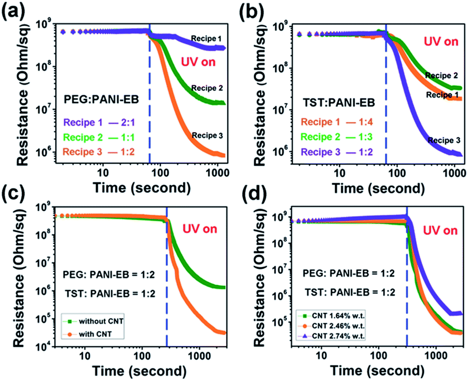 | ||
| Fig. 2 Response in resistance of the composite with changing the ratio of (a) PEG:PANI-EB and (b) TST:PANI-EB under UV irradiation (power: ∼40 mW cm−2); UV response in resistance of the composite with the optimized ratios of PEG:PANI-EB = 1:2 and TST:PANI-EB = 1:2 (c) with/without the introduction of CNTs at the weight ratio of 1.64%, and (d) with the introduction of CNTs at different weight ratios. | ||
This work is aiming to fabricate a kind of practical UV sensor and thus the corresponding accurate measurement under the outdoor UV exposure is essential. Fig. 3(a and b) show the whole sensor test setup placed in an outdoor parking lot and the as-prepared sensing patch. A laptop connected with a Keithley 2400 source meter were used to collect the testing data through the Matlab software. Meanwhile, a video was recorded to display the real-time change of the testing data under the irradiation from natural sunlight (Video S1, ESI†). Fig. 3(c) illustrates the UV index distribution of sunlight during the day time in which the UV index is defined as an open-ended linear scale which is directly proportional to the intensity of UV radiation. In this regard, the time dependent outdoor UV light conditions can be recognized as UV index of 7 in morning (9–11 am), 10 at noon (1–3 pm), 8 in afternoon (3–5 pm), and 0 at night (8–10 pm), respectively. Apparently, it only displays the risk level of the harm (low, moderate, high, very high or extreme), but not the degree of personal accumulative UV exposure. Then the normalized sheet resistance, (Rmax − R)/R (in which Rmax and R were denoted as the resistance of the sensing film pre/post UV exposures), of the prototype smart UV patch can be correlated with the above mentioned UV indexes at different time of a day, as plotted in Fig. 3(d). Evidently, due to the different reaction rates of the composite polymer under various UV indices of sunlight, that is the slower rate of PAG releasing H+ in the presence of weaker sunlight UV radiation, a smaller resistance change was characterized at lower UV indexes, e.g. 0, 7 or 8. Consistently, the resistance response of the composite polymer under the illumination of a light bulb (UV index = 0) shows no obvious change since the sensing film almost does not react with visible light irradiation. Additionally, the UV sensitivity of the as-fabricated composite polymer under the real sunlight which was consistent with the above testing in the UV box and further verify the feasibility of this unique design. It is also worthy to be noted that the composite polymer can stand much longer duration of exposure under natural sunlight irradiation compared to the test performed in a UV box, due to the relatively weak UV radiation in practical environment, which makes this smart sensor even more promising in real life applications. Temperature dependent stability is also a critical parameter to evaluable the applicability of an optical sensor. With this concern, the resistance stability of the composite polymer was investigated and compared before and after UV exposure at different temperatures. As shown in Fig. 3(e), with increasing the temperature from 40 to 100 °C, the sheet resistance of the as-prepared sensing polymer without exposing to UV light drops very quickly and linearly from 1010 to 106 Ω sq−1, while it does not present significant change after the UV exposure as depicted in Fig. 3(f). Hence, the as-fabricated composite polymer in this work is distinguishably stable at high temperatures under the illumination of solar light. Given the excellent irreversible and continual recording ability of the above as-prepared sensing polymer coated on flat glass substrates during the process of UV exposure, this concept was then employed to the flexible device configuration for better portability and compatibility with other devices. Also, further strategy needs to be proposed to solve the issue of the hardly read-out high initial resistance exhibited (∼109 Ω sq−1) in the above mentioned sensor device. In this regards, as illustrated in Fig. 4(a), a laser-induced graphene (LIG) film was introduced and firstly patterned on the surface of a flexible PI substrate (thickness: ∼100 μm)32 as the IDTs with the optimized area of ∼1.51 cm2 and width of ∼500 μm to maintain a minimum initial resistance or maximum resistance change in the optical sensor. As displayed in Fig. 4(b), the surface of the well-defined pattern of IDTs exhibits a foam-like appearance with a porous structure. Moreover, the Raman spectra as seen in Fig. 4(c) evidenced the successful fabrication of the single-layer graphene existing in the carbonized structure with the 2D vibrational mode just located at 2700 cm−1.33,34 Understandably, the successfully fabricated porous LIG structure can improve the electronic conductivities, and be helpful to enhance the accessible surface area, and thus facilitate the wetting between the electrode (i.e. IDTs) and the active materials. As evidenced in Fig. 4(d), the composite polymer solution can be evenly covered on the patterned PI substrate by a simple dip-coating method. Moreover, the EDS patterns of the IDTs' structures before and after polymer filling are also presented in Fig. S2 (ESI†) as a comparison. Consequently, as shown in Fig. 4(e), a largely improved UV sensitivity and dramatically reduced initial resistance (from 109 to 106 Ω) were accomplished in the sensing polymer fabricated on the PI substrate with patterned IDTs compared to those on the bare PI substrate and flat glass substrates shown in Fig. 2. Therefore, the conductivity of the supporting structure in a reasonable range plays a key factor to influence the whole working film sensitivity and especially in practical applications, the lower value of initial resistance is more favorable for the back-end circuit realization and easier detection of the UV signal. Interestingly, as displayed in Fig. 4(f), after exposure to UV light the polymer surface returned back to its original porous structure, which may be due to the occurrence of the PAG decomposition during the illumination process.35
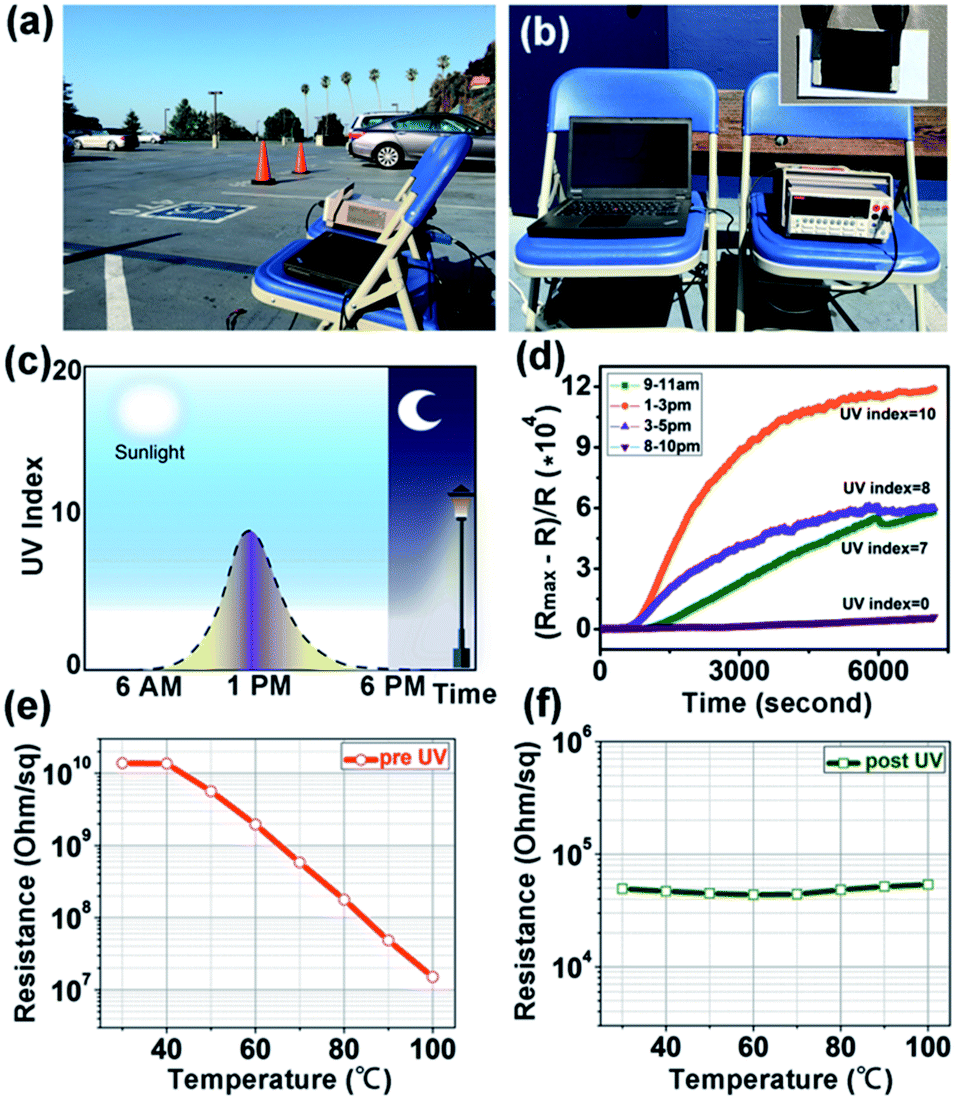 | ||
| Fig. 3 (a and b) Camera pictures of the outdoor test setup with the sensor film prepared on the glass substrate inserted in the inset of (b); (c) schematic illustration of a typical UV index distribution of sunlight during a day and (d) the corresponding UV sensitivity of the sensing film under the real sunlight monitored from the morning to night. Rmax and R were denoted as the resistance of the sensing film pre/post UV exposures; temperature dependence of sheet resistance (e) before and (f) after the UV exposures. | ||
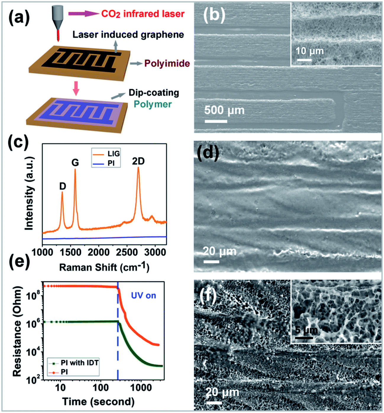 | ||
| Fig. 4 (a) Schematic illustration of the fabrication process of the composites on flexible polyimide (PI) substrates; (b) SEM images of the IDTs formed on the commercial PI substrate by using a CO2 laser source at a power of 4 W; (c) Raman spectra of the LIG film and the bare PI film; (d) SEM image of the morphology of the sensing composite before UV radiation; (e) UV sensitivity of the composite films prepared on the patterned and the bare flat PI substrates, respectively; (f) SEM image of the sensing composite after UV radiation with the high magnification image in the inset. | ||
Moreover, as shown in Fig. 5(a and b), to evaluate the wireless transmission function of the as-prepared composite, a custom-made flexible wireless copper coil (15-turns, 0.06 mm in diameter) of 115 μH (Ls) and a ceramic capacitor of 1 nF (C) were linked to the two interdigitated electrodes in parallel by a simple welding process. The size of the whole wireless readout circuit device is about 3.52 cm2 and can be placed on a human hand. Also, as illustrated Fig. 5(b), the LCR (inductance, capacitance, and resistance) meter (Agilent E4980) can conveniently, indirectly and wirelessly record the polymer impedance (Rx) change in real-time which is entirely different from the measurement carried out in the UV box as shown in Fig. S1(b) (ESI†). Fig. 5(c) shows the plot of phase angle (between the voltage and current) of the external readout versus time, which was measured under the UV source illumination. Also, the testing frequency was set to 465 kHz that resulted in the minimum phase and which is located in the minimum frequency near the secondary resonant frequency. During the entire ∼30 minutes of testing, the impedance phase obviously changed from 10° to almost 60°. After blocking the UV radiation, its value declined slightly and then stabilized, which again revealed the irreversible nature of the chemical reaction process in the smart sensing film. Furthermore, as depicted in Fig. 5(d), the measurements at multiple indoor and outdoor transitions were conducted with a two-minute interval. During the seven cycles of UV illumination, the reaction rate of the PAG in the first four cycles was rapid, and gradually decreased in the following cycles. This is consistent with the above results as shown in Fig. 2 and 5(c). In addition, during all the dark (UV off) process, the impedance phase angle experienced negligibly decrease which further verified the stable properties of this unique smart UV patch. Therefore, the resistance change of this smart sensing patch under UV irradiation can be successfully replaced and described by the phase angle change from the LCR meter. Consequently, by fabricating external portable micro-LCR meter and integrated with the watch, cell phone or other portable electronic devices which is promising way to accurately detect the UV irradiation dose from this disposable, non-polluting and low cost tiny UV patch.
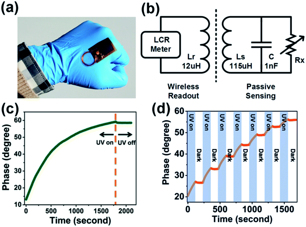 | ||
| Fig. 5 (a) Demonstration of the flexible UV smart patch attached on a human hand. (b) Schematic illustration of the simplified equivalent circuits of the outdoor wireless readout circuit and the UV sensing patch (Lr/Ls, C and Rx represent inductor, capacitor and resistance, respectively); (c) phase angle of external readout through wireless coil inductor under UV illumination; (d) phase angle of external readout measured under the multiple UV sensing cycles. | ||
4. Conclusion
In summary, a wearable, high sensitive, battery-free, and wireless UV patch was successfully fabricated to record the accumulative UV radiation in terms of resistance and phase angle. The introduction of the CNTs into the PANI-EB/PAG(TST)/PEG composite polymer solution effectively helps to enhance the range of the resistance change under the real sunlight exposure. Moreover, based on the facile laser induced graphene backbone technique and the following simplified dip-coating process, a flexible UV patch with lower initial resistance was further fabricated and optimized. Specially, the wireless detection was realized by integrating the entire flexible device with a copper coil and capacitor. The proposed sensing platform based on this unique tiny UV patch opens up a novel way to monitor the amount of excess UV exposure in natural sunlight and provides a concept design for further potential application.Conflicts of interest
There are no conflicts to declare.Acknowledgements
This work is supported in part by the DARPA SHIELD (Supply Chain Hardware Integrity for Electronics Defense) program with Agreement No. HR0011-15-C-0004. The authors would like to acknowledge financial support from the National Basic Research Program of China under Grant No. 2012CB933104, the National Science Fund of China under Grant No. 61271031, Sichuan Youth Science & Technology Fund under grant No. 2014JQ0010, Guangdong Innovative Research Team Program (No. 201001D0104713329) and the China Scholarship Council (CSC) scholarship under the State Scholarship Fund. Professor Liwei Lin is a core-principal investigator of the Tsinghua-Berkeley Shenzhen Institute (TBSI) and we acknowledge the funding support of TBSI.Notes and references
- H. Lee, T. K. Choi, Y. B. Lee, H. R. Cho, R. Ghaffari, L. Wang, H. J. Choi, T. D. Chuang, N. Lu, T. Hyeon, S. H. Choi and D. H. Kim, Nat. Nanotechnol., 2016, 11, 566–572 CrossRef CAS PubMed.
- W. Gao, S. Emaminejad, H. Y. Y. Nyein, S. Challa, K. Chen, A. Peck, H. M. Fahad, H. Ota, H. Shiraki, D. Kiriya, D. H. Lien, G. A. Brooks, R. W. Davis and A. Javey, Nature, 2016, 529, 509–514 CrossRef CAS PubMed.
- S. Xu, Y. Zhang, L. Jia, K. E. Mathewson, K. Jang, J. Kim, H. Fu, X. Huang, P. Chava, R. Wang, S. Bhole, L. Wang, Y. J. Na, Y. Guan, M. Flavin, Z. Han, Y. Huang and J. A. Rogers, Science, 2014, 344, 70–74 CrossRef CAS PubMed.
- D. H. Kim and N. Lu, et al., Science, 2011, 333, 838–843 CrossRef CAS PubMed.
- D. J. Lipomi and M. Vosgueritchian, et al., Nat. Nanotechnol., 2011, 6, 788–792 CrossRef CAS PubMed.
- K. Takei, T. Takahashi, J. C. Ho, H. Ko, A. G. Gillies, P. W. Leu, R. S. Fearing and A. Javey, Nat. Mater., 2010, 9, 821–826 CrossRef CAS PubMed.
- W. Wu, L. Wang, Y. Li, F. Zhang, L. Lin, S. Niu, D. Chenet, X. Zhang, Y. Hao, T. F. Heinz, J. Hone and Z. L. Wang, Nature, 2014, 514, 470–474 CrossRef CAS PubMed.
- M. Kaltenbrunner, T. Sekitani and J. Reeder, et al., Nature, 2013, 499, 458–463 CrossRef CAS PubMed.
- J. Liang, L. Li, X. Niu, Z. Yu and Q. Pei, Nat. Photonics, 2013, 7, 817–824 CrossRef CAS.
- S. Patel, H. Park, P. Bonato, L. Chan and M. Rodgers, J. NeuroEng. Rehabil., 2012, 9, 21 CrossRef PubMed.
- A. J. Bandodkar and J. Wang, Trends Biotechnol., 2014, 32, 363–371 CrossRef CAS PubMed.
- F. Urbach, J. Photochem. Photobiol., B, 1997, 40, 3–7 CrossRef CAS.
- M. K. Selgrade, M. H. Repacholi and H. S. Koren, Environ. Health Perspect., 1997, 105, 332 CrossRef CAS PubMed.
- H. R. Taylor, S. K. West, F. S. Rosenthal, B. Munoz, H. S. Newland, H. Abbey and E. A. Emmett, N. Engl. J. Med., 1988, 319, 1429–1433 CrossRef CAS PubMed.
- T. Tadokoro, N. Kobayashi, B. Zmudaka, S. Ito, K. Wakamatsu, Y. Yamaguchi, K. Korossy, S. Miller, J. Beer and V. J. Hearing, FASEB J., 2003, 17, 1177–1179 CAS.
- J. E. Cleaver and E. Crowley, Front. Biosci., 2002, 7, d1024–d1043 CAS.
- S. K. Panda and C. Jacob, Solid State Electron., 2012, 73, 44–50 CrossRef CAS.
- A. J. Gimenez, J. M. Yanez-Limon and J. M. Seminario, J. Phys. Chem. C, 2011, 115, 282–287 CAS.
- R. Copperwhite, C. McDonagh and S. O'Driscoll, IEEE Sens. J., 2012, 12, 1425–1426 CrossRef.
- A. Mills, M. McFarlane and S. Schneider, Anal. Bioanal. Chem., 2006, 386, 299–305 CrossRef CAS PubMed.
- J. Kim, G. A. Salvatore, H. Araki, A. M. Chiarelli, Z. Xie, A. Banks, X. Sheng, Y. Liu, J. W. Lee, K. Jang, S. Y. Heo, K. Cho, H. Luo, B. Zimmerman, J. Kim, L. Yan, X. Feng, S. Xu, M. Fabiani, G. Gratton, Y. Huang, U. Paik and J. A. Rogers, Sci. Adv., 2016, 2, 8 Search PubMed.
- H. Araki, J. Kim, S. Zhang, A. Banks, K. E. Crawford, X. Sheng, P. Gutruf, Y. Shi, R. M. Pielak and J. A. Rogers, Adv. Funct. Mater., 2017, 27, 2 Search PubMed.
- J. L. Dektar and N. P. Hacker, J. Am. Chem. Soc., 1990, 112, 6004 CrossRef CAS.
- M. A. Ratner and D. F. Shriver, Chem. Rev., 1988, 88, 109–124 CrossRef CAS.
- Q. Tang, J. Wu, Z. Tang, Y. Li and J. Lin, J. Mater. Chem., 2012, 22, 15836–15844 RSC.
- M. F. Shukur, M. F. Z. Kadir, Z. Ahmad and R. Ithnin, Adv. Mater. Res., 2012, 488, 583–587 CrossRef.
- A. C. Ibrahim, S. Devautour-Vinot, D. Naoufal and A. Mehdi, New J. Chem., 2012, 36, 1218–1223 RSC.
- C. Alber, Z. Shi, V. K. Johns, A. Lafave and Y. Liao, J. Appl. Polym. Sci., 2013, 129, 3546–3550 CrossRef CAS.
- J. C. Chiang and A. G. MacDiarmid, Synth. Met., 1986, 13, 193–205 CrossRef CAS.
- P. C. Ma, B. Z. Tang and J. K. Kim, Carbon, 2008, 46, 1497–1505 CrossRef CAS.
- E. N. Konyushenko, J. Stejskal, M. Trchova, J. Hradil, J. Kovarova, J. Prokes, M. Cieslar, J. Y. Hwang, K. H. Chen and I. Sapurina, Polymer, 2006, 47, 5715–5723 CrossRef CAS.
- J. Lin, Z. Peng, Y. Liu, F. R. Zepeda, R. Ye, E. L. G. Samuel, M. J. Yacaman, B. I. Yakobson and J. M. Tour, Nat. Commun., 2014, 5, 5714 CrossRef CAS PubMed.
- R. J. Nemanich and S. A. Solin, Phys. Rev. B: Condens. Matter Mater. Phys., 1979, 20, 392–401 CrossRef CAS.
- A. C. Ferrari, et al., Phys. Rev. Lett., 2006, 97, 187401 CrossRef CAS PubMed.
- D. Wen, Y. Liu, C. Yang, H. Liu, Y. Wu, X. Li, W. Cai, Y. Cui, B. Zhao, H. Zhang, F. Bai and L. Lin, in 19th International Conference on Solid-State Sensors, Actuators and Microsystems (TRANSDUCERS), IEEE, 2017, pp. 1144–1147 Search PubMed.
Footnote |
| † Electronic supplementary information (ESI) available. See DOI: 10.1039/c7ra10789g |
| This journal is © The Royal Society of Chemistry 2017 |