
 Open Access Article
 This Open Access Article is licensed under a
 Creative Commons Attribution 3.0 Unported Licence
Surfactant-mediated self-assembly of nanocrystals to form hierarchically structured zeolite thin films with controlled crystal orientation†
Chon Hei Lam‡
a,
Heng-Yu Chi‡a,
Shu-Ming Hsub,
Yun-Shiuan Lib,
Wen-Ya Lee c,
I-Chun Chengb and
Dun-Yen Kang*a
c,
I-Chun Chengb and
Dun-Yen Kang*a
aDepartment of Chemical Engineering, National Taiwan University, 1, Sec. 4, Roosevelt Road, Taipei 10617, Taiwan. E-mail: dunyen@ntu.edu.tw
bGraduate Institute of Photonics and Optoelectronics, National Taiwan University, 1, Sec. 4, Roosevelt Road, Taipei 10617, Taiwan
cDepartment of Chemical Engineering and Biotechnology, National Taipei University of Technology, 1, Sec. 3, Zhong-Xiao E. Rd., Taipei 10608, Taiwan
First published on 18th October 2017
Abstract
We report on a scalable wet deposition to simultaneously manipulate the self-assembly and orientation of zeolite Linde Type A (LTA) nanocrystals. This process, referred to as surfactant-mediated self-assembly (SMSA), creates zeolite LTA thin films with long-range ordered cylindrical patterns, wherein {100} faces of the crystals are preferably oriented parallel to the support surface. This approach makes it possible to control the diameter as well as the depth of the cylindrical patterns in zeolite thin films fabricated via scalable wet deposition. To elucidate the mechanism underlying the SMSA process, we applied in situ imaging to cast solutions subjected to a temperature swing. Our results indicate that the cylindrical patterns may be developed from micelles of the surfactant, which make up a thermodynamic phase in the cast solution. We also demonstrate that the apparent dielectric constant and optical haze of the zeolite LTA thin films can be engineered by altering the dimensions of the cylindrical patterns.
Introduction
Zeolites are nanoporous crystalline aluminosilicates used in a broad range of industrial applications.1–10 Over the last two decades, revolutionary advances in zeolite engineering have led to the fabrication of zeolite thin films/membranes11–28 as well as the creation of hierarchical structures4,29–35 within zeolite particles. The ability to engineer zeolite crystals as a thin film or a membrane has opened up new opportunities in the fields of membrane separation,36–45 membrane reactors,46–54 and thin-film-based electronics.24,55–58 Hierarchically structured zeolites represent a bridge between conventional bulk zeolites and meso/macroporous aluminosilicates, achieving unique properties for highly specific applications.59–63 For instance, zeolite particles have been used in the development of advanced catalysts with high shape selectivity (attributed to the microporosity) and reduced internal mass transfer resistance (attributed to the mesoporosity).59 Despite considerable advances in the development of hierarchically structured zeolite particles, researchers have not yet to establish a self-assembly-based (bottom-up) method for the deposition of hierarchically structured zeolite thin films/membranes on non-templated substrates.Relatively few reports have described top-down techniques for the patterning of zeolite thin films, and most of these have involved electron beam lithography or photolithography.17,64,65 Electron beam lithography has been used to create square patterns of 10 × 10 mm on thin films comprising zeolite A and silicalite to enable the selective adsorption of bovine serum albumin.64 Several studies have described bottom-up techniques for the structuring of zeolite thin films.17,27,66,67 It has been demonstrated that organic functional groups tethered on a glass substrate can be used for the transfer of patterns to cast ZSM-5 films.66,67 Micromolding has been implemented using a patterned polydimethylsilane (PDMS) stamp for the structuring of silicalite thin films.27 However, all existing bottom-up techniques require a pre-patterned substrate or mold.
In this paper, we report on a novel bottom-up method, referred to as surfactant-mediated self-assembly (SMSA), for the fabrication of mesostructured zeolite thin films with controlled crystal orientation. This method allows for large-scale deposition of structured zeolite thin films on pattern-free substrates. The proposed method of SMSA involves the formation of surfactant micelles in the cast solution. The zeolite depletion phase (comprising the surfactant-solvent micelle) in the cast solution ultimately forms into patterns in the zeolite thin films. As a proof of concept, we utilized the SMSA to fabricate zeolite Linde Type A (LTA) thin films with ordered cylindrical patterns, wherein the {100} faces of zeolite LTA nanocrystals were oriented to parallel the support surface (Fig. 1). The zeolite LTA discussed in this study was formulated at a Si![[thin space (1/6-em)]](https://www.rsc.org/images/entities/char_2009.gif) :Al ratio of 3:1. TWEEN® 80 was used as the surfactant for SMSA. We demonstrated that the diameter as well as the depth of the cylindrical patterns in the zeolite thin films can be precisely controlled by the experimental conditions of SMSA. In situ imaging was performed to capture the dynamics of assembly of zeolite nanocrystals. We also showed that the apparent dielectric and optical properties of the zeolite LTA thin films can be engineered by the mesostructure of the thin films.
:Al ratio of 3:1. TWEEN® 80 was used as the surfactant for SMSA. We demonstrated that the diameter as well as the depth of the cylindrical patterns in the zeolite thin films can be precisely controlled by the experimental conditions of SMSA. In situ imaging was performed to capture the dynamics of assembly of zeolite nanocrystals. We also showed that the apparent dielectric and optical properties of the zeolite LTA thin films can be engineered by the mesostructure of the thin films.
Results and discussion
The photographic image of zeolite LTA cast solutions is presented in the ESI (Fig. S1†). The zeolite LTA film cast from the solution with a TWEEN® 80 concentration of 6.67 wt% is referred to as LTA-6.67, and the remaining samples are named by analogy. Spin cast was employed to deposit the zeolite LTA films on a silicon wafer or glass substrate. Following calcination, the zeolite LTA thin films were approximately 300 nm in thickness (Fig. 1). The thin films with cylindrical patterns were composed of nearly spherical zeolite LTA crystals with a size of approximately 100 nm.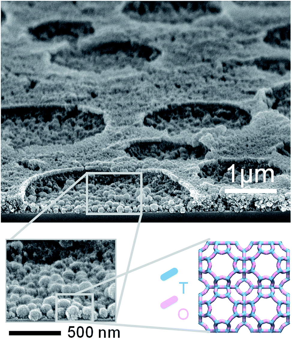 | ||
| Fig. 1 (Top) Tilt SEM image of LTA-6.67 cast on a silicon wafer substrate, showing that the zeolite LTA thin film comprises zeolite LTA crystals of approximately 100 nm in diameter. In this image, the interface between the thin film and substrate can be clearly observed. (Bottom) The illustration shows the topology of zeolite LTA as well as its orientation with respect to the substrate, wherein the T atoms are tetrahedral silicon or aluminum, and the O atoms are oxygen. | ||
The crystallinity and crystal orientation of the deposited zeolite LTA films was investigated by grazing-incidence wide-angle X-ray scattering (GIWAXS) (Fig. 2a and b). The GIWAXS pattern of the silicon wafer substrate is presented in the ESI (Fig. S2a†). To confirm the existence of zeolite LTA phase, the raw 2D GIWAXS patterns were reduced to 1D patterns and were compared the simulated powder XRD pattern (Fig. 2c). Both LTA-3.34 and LTA-6.67 possessed the characteristic XRD pattern of zeolite LTA. The azimuthal intensity profiles (intensity profile in χ-direction) of the first four diffractions ({100}, {110}, {111}, and {210}) in the 2D GIWAXS pattern are shown in Fig. 2d to analyze the preferred orientation of zeolite LTA crystals in the thin films. The highest intensity of these four peaks occurred at 0, −45, −55, and −22°, respectively. The results indicate that the {100} faces of zeolite LTA nanocrystals in the thin films were oriented to parallel the support surface. However, the highest intensity of {210} diffraction should theoretically be at −27° instead of −22°. The observed shift was likely due to the relatively low signal-to-noise ratio of {210} diffraction. In contrast, the intensity in the GIWAXS pattern of LTA-0 showed uniform distribution along the azimuthal direction (ESI, Fig. S2†), which indicates no preferred orientation of the zeolite LTA crystals in the thin film. The results suggest that the presence of a surfactant may be the key for the control of crystal orientation. Compared to the existing techniques for controlling crystal orientation in zeolite thin films/membranes,38,68–70 our proposed method considerably simplifies the fabrication process.
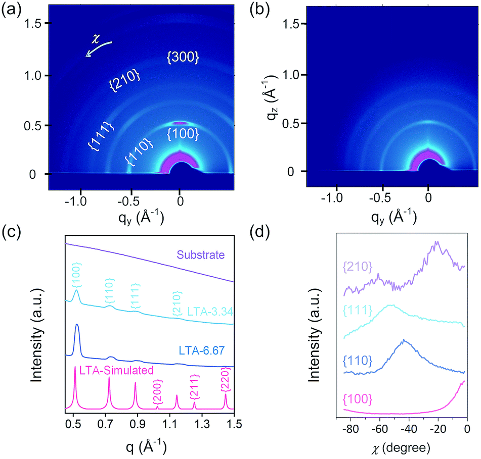 | ||
| Fig. 2 (a) 2D GIWAXS pattern of LTA-6.67. (b) 2D GIWAXS pattern of LTA-3.34. (c) X-ray scattering intensity profiles integrated along the azimuthal direction of the raw 2D GIWAXS patterns and the simulated powder XRD pattern of zeolite LTA. (d) The intensity profiles of the first four diffractions of LTA-6.67 as a function of the azimuthal angle (χ) indicate a preferred orientation of zeolite LTA crystal in this thin film sample. The direction of χ = 0° coincides with the positive qz direction, and that of χ = −90° coincides with negative qy direction. | ||
The size of the cylindrical pattern can be controlled by adjusting the concentration of TWEEN® 80 in the cast solution. Fig. 3 presents top-view images obtained from optical microscope (OM) and scanning electron microscope (SEM), showing zeolite LTA thin films formed from cast solution with a TWEEN® 80 concentration of 3.34, 6.67, or 9.67 wt% (corresponding to a TWEEN® 80-to-Si molar ratio of 0.039, 0.078, and 0.118, respectively). The substrate used in the preparation of this set of samples was a silicon wafer with a water contact angle of 35°.
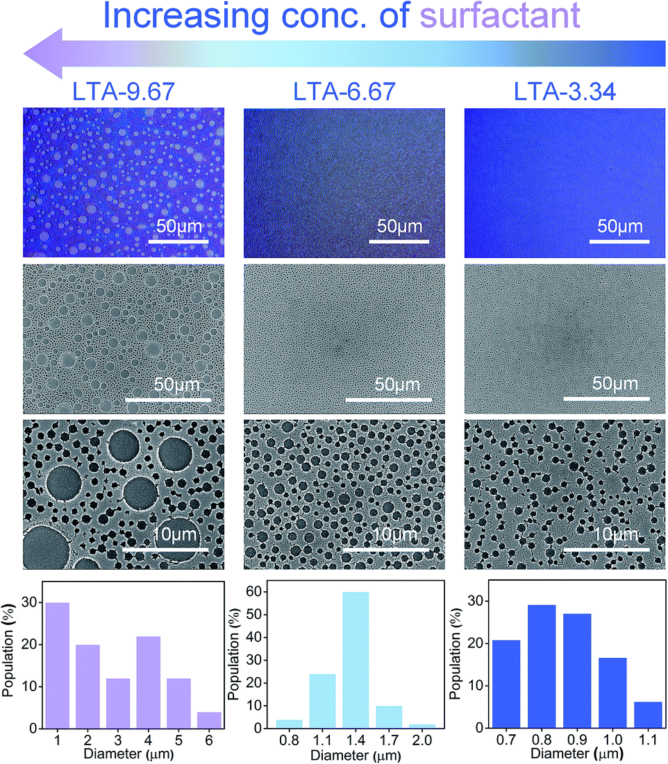 | ||
| Fig. 3 OM (first row) and SEM (second and third row) images of the zeolite LTA thin films and a statistical summary (last row) of the size of cylindrical patterns formed in the thin films. The thin films were cast on a silicon wafer substrate with a water contact angle of 35° from aqueous colloidal suspensions that included the surfactant, TWEEN® 80, at various concentrations. | ||
It was found that the size of the cylindrical patterns increased with the concentration of TWEEN® 80 in the cast solutions. On each of the three samples (LTA-3.34, LTA-6.67, and LTA-9.67), cylindrical patterns appeared over a large area of the thin film, rather than over a local area. The SEM images presented in Fig. 4 highlight the cylindrical patterns with long-range order. The size distributions of the patterns in each sample are also shown in Fig. 3. The pattern diameter of LTA-3.34 ranged from 0.7 to 1.1 μm, whereas that of LTA-6.67 ranged from 0.9 to 1.9 μm. Both samples presented a narrow distribution of pattern sizes. However, we observed a bimodal distribution in the pattern size of LTA-9.67, resulting in patterns with a diameter exceeding 5 μm. The patterns in the LTA-0 and LTA-12.5 samples in the ESI (Fig. S3†) were poorly defined.
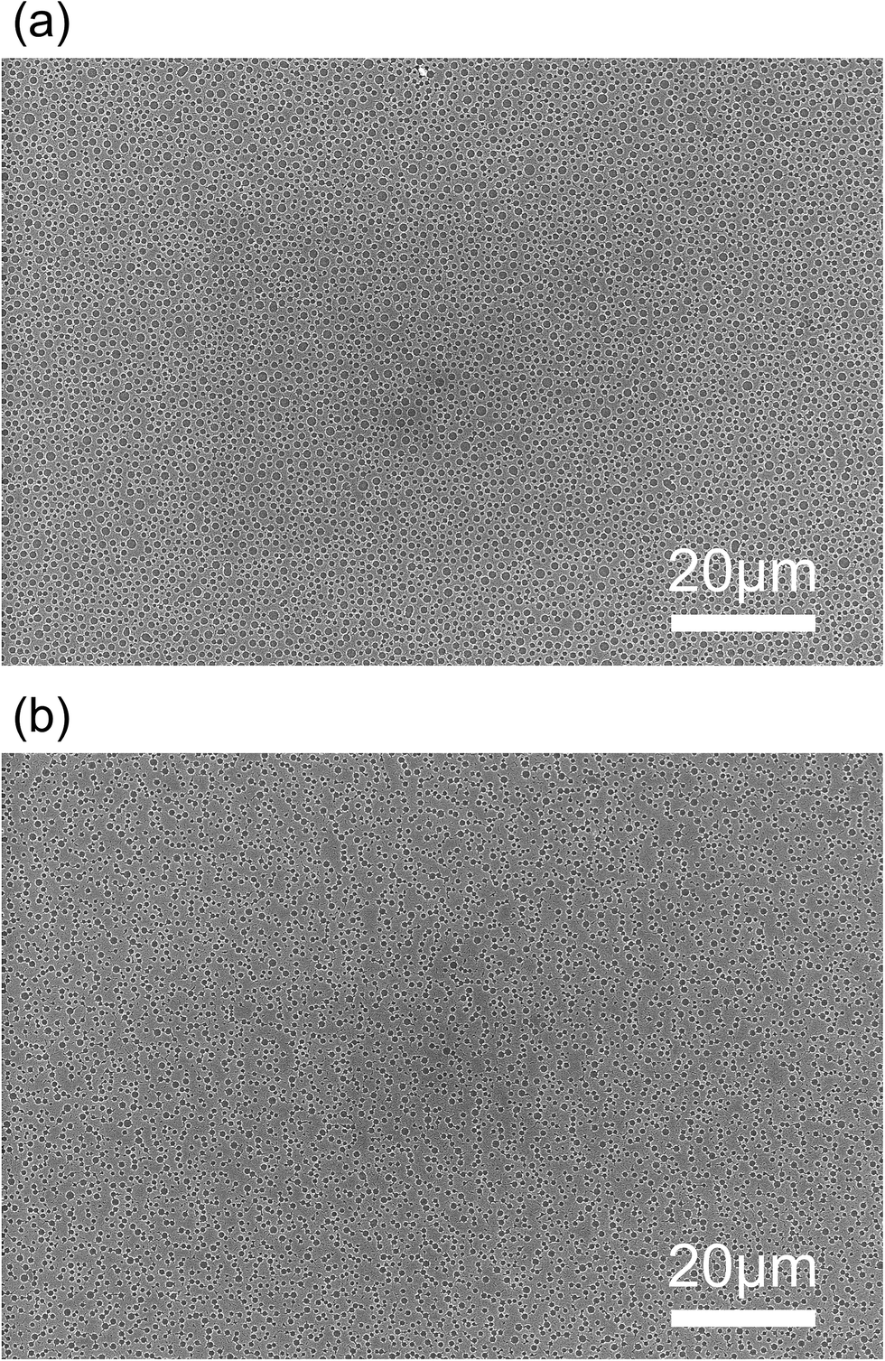 | ||
| Fig. 4 Low-magnification SEM images of (a) LTA-6.67 and (b) LTA-3.34. These images suggest that the LTA thin films possess long-range ordered cylindrical patterns. | ||
In addition to the diameter control, we were also able to tailor the depth of the cylindrical patterns in the zeolite LTA thin films simply by adjusting the surface hydrophilicity of the substrate. The substrate with higher hydrophilicity (water contact angle = 35°) produced LTA thin films with shallower cylindrical patterns (Fig. 5a). Depositing the same cast solution on the silicon wafer with the lower hydrophilicity (water contact angle = 54°) produced cylindrical patterns that pierced the LTA films and left the substrate partially uncovered (Fig. 5b). The pattern size distributions of the zeolite thin film cast on the relatively hydrophobic Si wafer substrate are shown in ESI (Fig. S4†). The difference in the pattern depth could be attributed to the relative hydrophilicity of the zeolite LTA particles and the micelles formed by the surfactant and the solvent (water). Specifically, we hypothesize that the micelle was formed by water surrounded by the hydrophilic groups of TWEEN® 80, whereas the exterior surface of the micelle comprises hydrophobic groups of the surfactant. The hydrophobic nature of the micelle surface caused the micelles to wet the surface of the hydrophobic silicon wafer, which may explain why the patterns pierced the zeolite LTA films on a relatively hydrophobic substrate. Fig. 5 (right column) illustrates the proposed scheme described above. To test our hypothesis, we used a glass substrate with a water contact angle of 42°, similar to that of the hydrophilic silicon wafer for the deposition of thin films. The resulting cylindrical patterns which is showed in the ESI (Fig. S5†) did not pierce the films. The shape of the patterns in the LTA films on a glass substrate was not as uniform as that seen in films on a silicon wafer, due to the fact that the surface of the glass substrate is rougher than that of the silicon. This indicates that the experiments using the glass substrate cannot fully compare with those using the silicon wafer substrate.
 | ||
| Fig. 5 (a) A relatively hydrophilic substrate yielded shallow patterns. (b) A relatively hydrophobic substrate yielded patterns that pierced the substrate. The proposed schemes underlying the formation of surfactant micelles in solutions spin cast on the two substrates are illustrated in the right-bottom of corners of (a) and (b). | ||
An in situ investigation was conducted by using an optical microscope to gain insight into the formation of patterns in the zeolite LTA films via surfactant-mediated self-assembly (SMSA). Specifically, we filmed the suspension that formed the LTA-3.34 when spin cast on a silicon wafer substrate subject to a temperature swing between 15 to 80 °C. A video clip from this experiment has been appended in the ESI (Video S1†), and representative snapshots are presented in Fig. 6. The as-cast solution at 15 °C appeared entirely featureless, which suggests that the entire system formed a homogeneous phase. Dot patterns appeared when the temperature was increased to 80 °C, indicating the occurrence of phase separation.
 | ||
| Fig. 6 Snapshots of spin cast zeolite LTA-3.34 suspension subject to a temperature swing. The scale bar for the snapshots represents 20 μm. The dot patterns observed at 105 s and 416 s are probably a surfactant-rich phase formed by the surfactant micelle, which ultimately formed cylindrical voids in the zeolite LTA thin films following calcination. | ||
The dimensions of the dot patterns observed in the cast solution were close to those of the cylindrical patterns observed in calcined zeolite LTA thin films. Thus, we suspect that the pattern of dispersed dots in the cast solution was a surfactant-rich phase formed by micelles of the surfactant, which was burned off during calcination leaving cylindrical voids in the thin films. We surmise that the continuous phase in the cast solution may be a zeolite-rich phase, due to the fact that it remained even after high-temperature calcination.
Interestingly, we found that SMSA can be controlled thermodynamically. The dot patterns disappeared when the temperature was lowered from 80 °C to 15 °C, as shown in the snapshot obtained at 306 s (Fig. 6). The dot patterns re-appeared when the temperature was brought back to 80 °C, as shown in the snapshot obtained at 416 s (Fig. 6). The reversibility of the micelle formation during the temperature swing suggests that the surfactant micelle is very likely to be a thermodynamic phase. Nonetheless, the three snapshot images of the cast solution obtained at 15 °C (Fig. 6) appear similar but are not identical. Furthermore, the two snapshot images of the cast solution obtained at 80 °C (Fig. 6) were not completely identical either. This might be due to the persistent evaporation of the solvent (water) from the cast solution throughout the experiment, which resulted in variations in the composition of the cast solution.
To evaluate the effectiveness of SMSA in engineering the electrical and optical properties of zeolite LTA thin films, we performed measurements on the dielectric constant, transmission, and reflection haze. Fig. 7 summarizes the dielectric constants (εr) of three zeolite LTA thin film samples (LTA-9.67, LTA-6.67, and LTA-3.34) at frequencies ranging from 1 to 1000 kHz. Fig. S6† illustrates the architecture of the device for the measurements. These samples were deposited on a silicon wafer substrate with a water contact angle of 54°.
 | ||
| Fig. 7 Dielectric constants of various zeolite LTA thin films. These results demonstrate that the apparent electrical properties can be controlled by varying the size of the cylindrical patterns created in the thin films. | ||
The εr value of all tested samples decreased monotonically with frequency, which is common in dielectric materials. LTA-9.67 presented considerably higher mean εr values and a larger standard deviation than did the other two samples. This was probably due to the large size of the cylindrical patterns (relative to LTA-6.67 and LTA-3.34), which could cause current leakage. The patterns on LTA-9.67 also presented a broad size distribution, which may account for the large standard deviation in the values for εr. The small standard deviation in εr in the LTA-6.67 and LTA-3.34 samples suggests that almost no current leakage occurred during the measurements. The εr of a zeolite crystal is considered an intrinsic property governed by the topology as well as the composition. LTA-3.34 and LTA-6.67 present an identical topology and composition; however, the εr values are different. The average size of the cylindrical patterns in LTA-3.34 was approximately 0.5 μm smaller than the patterns observed in LTA-6.67, which suggests that micrometer-sized patterns may alter the apparent εr of zeolite thin films. The dielectric constants of LTA-0 and LTA-12.5 were also measured (ESI, Fig. S7†). Both samples showed εr values with large standard deviation. It was likely because a number of defects presented in these samples, which caused high leakage current during the measurements.
Zeolite LTA films were cast on glass substrate to enable the tuning of substrate transparency (Fig. 8). The OM and SEM images of the tested samples are presented in the ESI (Fig. S5†). The results of haze measurements showed that the bare glass substrate produced negligible transmission haze and less than 30% reflection haze in the visible light region. Transmission haze and reflection haze were both shown to increase following the deposition of a zeolite LTA film on the substrate. We investigated three samples in which the zeolite LTA thin film samples (LTA-12.5, LTA-9.67, and LTA-6.67) were deposited on a glass substrate. LTA-6.67 presented the smallest cylindrical patterns as well as the highest transmission haze and reflection haze. Transmission haze and reflection haze were both shown to decrease with an increase in the size of the patterns. This can be attributed to the fact that surface features with lateral auto correlation lengths at scale of several micrometers are less prone to light scattering, thereby reducing the haze produced in the visible light region.71 Finally, to assess the physical adhesion between the zeolite thin films and the substrate, we blew the thin film samples with high-pressure nitrogen. We found that the microstructure in the thin films stayed unchanged after the high-pressure treatment (ESI, Fig. S8†).
 | ||
| Fig. 8 Transmission haze and reflection haze of various zeolite LTA thin films. These results demonstrate that the apparent optical properties can be controlled by varying the size of the cylindrical patterns created in the thin films. | ||
Conclusions
The surfactant-mediated self-assembly (SMSA) method proposed in this paper represents a remarkable step toward manipulating zeolite crystals as well as other classes of nanocrystals to form patterned thin films via wet deposition. This thermodynamically controlled technique is capable of directing the self-assembly of zeolite LTA nanocrystals to form cylindrical patterns with long-range order. Furthermore the crystal orientation can be controlled in situ during thin film deposition. The proposed SMSA method avoids the tedious procedures involved in existing top-down patterning techniques, and it offers a new route by which to tune the extrinsic dielectric as well as optical properties of mesostructrued thin films formed of nanocrystals. Using the SMSA method, the thin films possessing patterns with size gradient may be prepared for cell culture.Experimental section
Chemicals
Sodium hydroxide (98 wt%), LUDOX HS-30 colloidal silica (30 wt%), aluminum isopropoxide (98 wt%), TWEEN® 80, hydrogen peroxide (30 wt%), sulfuric acid (95 wt%), and hydrochloric acid (37 wt%) were purchased from Sigma Aldrich. Tetramethylammonium hydroxide solution (TMAOH 25 wt% in water) was purchased from Merck. Triethoxy(octyl)silane (97 wt%) and toluene (99 wt%) were purchased from Acros. The deionized water used for the synthesis was purified using the Thermo Scientific™ Barnstead™ NANOpure® DIamond™ analytical ultrapure water system.Synthesis of zeolite LTA cast solution
0.13 g of sodium hydroxide (98 wt%) was dissolved in 7.9 g of deionized water at room temperature in a paraformaldehyde (PFA) container. This solution was then mixed with 25.4 g of tetramethylammonium hydroxide (TMAOH) solution (25 wt% in water) to form a mixture of NaOH–H2O–TMAOH weighing 33.4 g, of which 16.7 g was mixed with 5.8 g of LUDOX HS-30 colloidal silica (30 wt% suspension in water). The resulting suspension was agitated at 298 K in a PFA container for 3 h. The remaining 16.7 g of NaOH–H2O–TMAOH mixture was added with 2.0 g of aluminum isopropoxide (98 wt%) and the resulting mixture was agitated at 298 K in a PFA container for 3 h. The two mixtures (with a silicon source and with an aluminum source) were mixed and aged at room temperature for 24 h under agitation. The entire mixture produced a mass of 41.2 g with the following molar ratio: Al2O3:SiO2:Na2O:(TMA)2O:H2O = 1:6:0.32:7.27:350. We transferred 7.0 g of the aged solution to a 10 mL sealed vial made of glass (IntelliVent™ Reaction Vial System) for the hydrothermal reaction, which was conducted using a microwave oven (CEM Discover® Personal Synthesizer with LabMate™ System). The hydrothermal synthesis process was conducted at 353 K for 45 minutes under agitation. To maintain a constant reaction temperature during synthesis, the power of the microwave radiation was varied between 2 and 5 W. After the microwave assisted synthesis, a solution containing zeolite LTA nanoparticles formed during the hydrothermal reaction. Various quantities of the surfactant TWEEN® 80 (0, 0.25, 0.5, 0.75, or 1.0 g) was subsequently added to 7 g of the premade zeolite LTA suspension. The resulting mixtures were then stirred vigorously for 24 h to form uniform cast solutions with 0, 3.34, 6.67, 9.67, or 12.5 wt% of TWEEN® 80. The cast solutions with 0, 3.34, 6.67, 9.67, or 12.5 wt% of TWEEN® 80 resulted in TWEEN® 80-to-Si molar ratios of 0, 0.039, 0.078, 0.118, and 0.158, respectively.
Deposition of zeolite LTA thin films
Cast solutions with 0, 3.34, 6.67, 9.67, or 12.5 wt% of TWEEN® 80 were deposited on a silicon wafer substrate using a spin coater (Laurell Model-WS-650M2-23NPPB). Two types of silicon wafer (differing only in hydrophilicity) and one type of glass substrate were used in this study. Both silicon wafer substrates were purchased from SUMMIT-TECH Resource Corp. The relatively hydrophilic silicon wafer presented resistivity of 1.5–100 ohm-cm, whereas the relatively hydrophobic silicon wafer presented resistivity of less than 0.0015 ohm-cm. Both silicon wafer substrates were P-boron type with native oxide and orientation of (100) ±0.5 degree. The glass substrates (Corning® EXG Taiwan) were cleaned using piranha solution (1:1 30% H2O2 in H2O:H2SO4) before spin coating. The cast solution was dropped until it covered the entire substrate and then spin cast at 2000 rpm for 30 s. Another layer of the cast solution was subsequently dropped on the same substrate and subjected to spin coating under the same spin conditions and duration. Substrates covered with a thin layer of cast solution were then transferred to a furnace (pre-heated to 80 °C) for the removal of solvent and organic moieties. The thin film samples were baked at 80 °C for 1 h, after which the temperature was increased to 450 °C (heating ramp: 1 °C min−1) and held there for 5 h. This led to the formation of a solid-state thin film on the substrates. The thin film samples then underwent direct material characterization using optical microscopy, scanning electron microscopy, X-ray diffraction, and UV-vis-NIR reflectance spectroscopy. Surface modification aimed at increasing the hydrophobicity of the samples was conducted to facilitate the measurement of the dielectric constant. The surface modification procedure is described in the following section.
Surface modification of zeolite LTA thin films
Triethoxy(octyl)silane (OTES) was used to modify the surface of the samples in order to increase the hydrophobicity of the LTA films. Prior to modification, the LTA thin films were immersed in hydrochloric acid (HCl) for 20 min. The OTES solution was prepared by mixing 3 mL of OTES (97 wt%) with 30 mL of toluene. The acid-treated LTA films were immersed in the OTES solution at 90 °C for 90 min before being rinsed in toluene and dried using a high-pressure nitrogen gun. The thin film samples were then baked at 150 °C in a furnace before measuring the electrical properties.Material characterization
A Hitachi S4800 field emission scanning electron microscope (SEM) was used to characterize the morphology of the thin film samples. The samples were coated with platinum via sputtering deposition at an acceleration voltage of 25 V for 40 s. SEM imaging was conducted at an acceleration voltage of 10 kV.An optical microscope (Whited WM-100) was used to image the thin film samples as well as the solutions spin cast on the substrates. The same microscope was used for the real-time imaging of surfactant-mediated self-assembly (SMSA) occurring within the cast solutions on the substrates.
GISAXS patterns were obtained using the facilities at beamline 13A station at the National Synchrotron Radiation Research Center (NSRRC) in Taiwan. We employed incidence X-ray with energy of 12.12 keV (1.0227 Å). A sample-to-detector distance of 335.67 mm was opted. The incidence angle of each X-ray beam was 0.5027°. Scattering patterns were recorded using a Bicron point detector (Mar165 CCD) with 8 to 10 s of exposure. The raw scattering patterns were processed using GIXSGUI.72
The water contact angle of the substrate was determined using a contact angle analyzer (FTA125, First Ten Angstroms, Inc.). Two measurements were performed on each sample.
To fabricate the device (ESI, Fig. S6†) for the measurements of relative permittivity (dielectric constant) of zeolite thin films, physical vapor deposition (PVD) was first used to deposit gold electrodes on the samples. The pressure in the vacuum chamber was first lowered to less than 10−5 Torr. A rotary table (operating at 10 rpm) was used for the placement of samples. The operating voltage of the gold heater was 70 V, resulting in a gold deposition rate of 1.2 Å s−1. The final thickness of the gold electrode was 100 nm. The capacitance was measured using a Keysight 4284A Precision LCR meter under a bias voltage of 1 V. Measurements were conducted at frequencies of 1, 10, 100, and 1000 kHz. The dielectric constant (εr) of the thin films was calculated using the relation εr = Cd/ε0A, where C is the measured capacitance, d is the thickness (determined from cross-sectional SEM images), A is the area of the deposited electrode (2 mm2), and ε0 is the vacuum permittivity (8.85 × 10⁻¹² F m−1).
The UV-vis-NIR transmittance and reflectance spectra of the LTA thin films on glass substrates was measured by using a UV-vis-NIR spectrophotometer (V-670, Jasco, Japan). The wavelength range was 300 nm to 800 nm and the scanning rate was 1000 nm min−1. The total transmission and reflectance spectra were measured with the samples held normal to the incident beam. Transmission haze values were calculated according to the ratio of diffuse transmittance to total transmittance, and the reflection haze value was defined as the ratio of reflected light spreading 5° from specular reflections to the total reflection.
Conflicts of interest
There are no conflicts to declare.Acknowledgements
This work was supported by the Ministry of Science and Technology (MOST) of Taiwan (MOST 104-2628-E-002-009-MY3 and MOST 105-2221-E-002-056-MY2). We would like to thank Chin-Yan Lin and Ya-Yun Yang at the Electron Microscope Unit of Instrument Center at National Taiwan University for their valuable assistance in obtaining SEM images. We also acknowledge the scientists at beamline 13A in National Synchrotron Radiation Research Center (NSRRC) of Taiwan for the assistance in GIWAXS measurements.Notes and references
- J. Gascon, F. Kapteijn, B. Zornoza, V. Sebastian, C. Casado and J. Coronas, Chem. Mater., 2012, 24, 2829–2844 CrossRef CAS.
- V. Valtchev and L. Tosheva, Chem. Rev., 2013, 113, 6734–6760 CrossRef CAS PubMed.
- C. M. A. Parlett, K. Wilson and A. F. Lee, Chem. Soc. Rev., 2013, 42, 3876–3893 RSC.
- I. I. Ivanova and E. E. Knyazeva, Chem. Soc. Rev., 2013, 42, 3671–3688 RSC.
- J.-H. Lee, Sens. Actuators, B, 2009, 140, 319–336 CrossRef CAS.
- N. Yu, R. Z. Wang and L. W. Wang, Prog. Energy Combust. Sci., 2013, 39, 489–514 CrossRef.
- D. P. Serrano, J. Aguado and J. M. Escola, ACS Catal., 2012, 2, 1924–1941 CrossRef CAS.
- M. Moliner, C. Martinez and A. Corma, Angew. Chem., Int. Ed., 2015, 54, 3560–3579 CrossRef CAS PubMed.
- T. Ennaert, J. Van Aelst, J. Dijkmans, R. De Clercq, W. Schutyser, M. Dusselier, D. Verboekend and B. F. Sels, Chem. Soc. Rev., 2016, 45, 584–611 RSC.
- V. Van Speybroeck, K. Hemelsoet, L. Joos, M. Waroquier, R. G. Bell and C. R. A. Catlow, Chem. Soc. Rev., 2015, 44, 7044–7111 RSC.
- M. G. Buonomenna, Desalination, 2013, 314, 73–88 CrossRef CAS.
- W. G. Kim and S. Nair, Chem. Eng. Sci., 2013, 104, 908–924 CrossRef CAS.
- S. S. Shenvi, A. M. Isloor and A. F. Ismail, Desalination, 2015, 368, 10–26 CrossRef CAS.
- S. Daer, J. Kharraz, A. Giwa and S. W. Hasan, Desalination, 2015, 367, 37–48 CrossRef CAS.
- C. Mousty and A. Walcarius, J. Solid State Electrochem., 2015, 19, 1905–1931 CrossRef CAS.
- S. Shaikhutdinov and H. J. Freund, J. Phys.: Condens. Matter, 2015, 27, 15 CrossRef PubMed.
- S. Mandal, H. L. Williams and H. K. Hunt, Microporous Mesoporous Mater., 2015, 203, 245–258 CrossRef CAS.
- M. A. Mir, M. A. Bhat, R. A. Naikoo, R. A. Bhat, M. Khan, M. Shaik, P. Kumar, P. K. Sharma and R. Tomar, Sens. Actuators, B, 2017, 242, 1007–1020 CrossRef CAS.
- G. F. Fine, L. M. Cavanagh, A. Afonja and R. Binions, Sensors, 2010, 10, 5469–5502 CrossRef CAS PubMed.
- K. P. Lee, T. C. Arnot and D. Mattia, J. Membr. Sci., 2011, 370, 1–22 CrossRef CAS.
- K. Varoon, X. Y. Zhang, B. Elyassi, D. D. Brewer, M. Gettel, S. Kumar, J. A. Lee, S. Maheshwari, A. Mittal, C. Y. Sung, M. Cococcioni, L. F. Francis, A. V. McCormick, K. A. Mkhoyan and M. Tsapatsis, Science, 2011, 334, 72–75 CrossRef CAS PubMed.
- H. Y. Chen, J. Wydra, X. Y. Zhang, P. S. Lee, Z. P. Wang, W. Fan and M. Tsapatsis, J. Am. Chem. Soc., 2011, 133, 12390–12393 CrossRef CAS PubMed.
- N. Ma, J. Wei, R. H. Liao and C. Y. Y. Tang, J. Membr. Sci., 2012, 405, 149–157 CrossRef.
- C. M. Lew, R. Cai and Y. Yan, Acc. Chem. Res., 2010, 43, 210–219 CrossRef CAS PubMed.
- M. L. Lind, D. E. Suk, T. V. Nguyen and E. M. V. Hoek, Environ. Sci. Technol., 2010, 44, 8230–8235 CrossRef CAS PubMed.
- M. T. M. Pendergast, J. M. Nygaard, A. K. Ghosh and E. M. V. Hoek, Desalination, 2010, 261, 255–263 CrossRef CAS.
- L. Huang, Z. Wang, J. Sun, L. Miao, Q. Li, Y. Yan and D. Zhao, J. Am. Chem. Soc., 2000, 122, 3530–3531 CrossRef CAS.
- S. Claes, P. Vandezande, S. Mullens, K. De Sitter, R. Peeters and M. K. Van Bael, J. Membr. Sci., 2012, 389, 265–271 CrossRef CAS.
- D. Verboekend and J. Perez-Ramirez, Catal. Sci. Technol., 2011, 1, 879–890 CAS.
- K. H. Li, J. Valla and J. Garcia-Martinez, ChemCatChem, 2014, 6, 46–66 CrossRef CAS.
- A. Inayat, B. Reinhardt, H. Uhlig, W. D. Einicke and D. Enke, Chem. Soc. Rev., 2013, 42, 3753–3764 RSC.
- W. Schwieger, A. G. Machoke, T. Weissenberger, A. Inayat, T. Selvam, M. Klumpp and A. Inayat, Chem. Soc. Rev., 2016, 45, 3353–3376 RSC.
- W. J. Roth, B. Gil, W. Makowski, B. Marszalek and P. Eliasova, Chem. Soc. Rev., 2016, 45, 3400–3438 RSC.
- D. Schneider, D. Mehlhorn, P. Zeigermann, J. Karger and R. Valiullin, Chem. Soc. Rev., 2016, 45, 3439–3467 RSC.
- Z. X. Qin, J. P. Gilson and V. Valtchev, Curr. Opin. Chem. Eng., 2015, 8, 1–6 CrossRef.
- N. Rangnekar, N. Mittal, B. Elyassi, J. Caro and M. Tsapatsis, Chem. Soc. Rev., 2015, 44, 7128–7154 RSC.
- M. A. Snyder and M. Tsapatsis, Angew. Chem., Int. Ed., 2007, 46, 7560–7573 CrossRef CAS PubMed.
- Z. Lai, G. Bonilla, I. Diaz, J. G. Nery, K. Sujaoti, M. A. Amat, E. Kokkoli, O. Terasaki, R. W. Thompson, M. Tsapatsis and D. G. Vlachos, Science, 2003, 300, 456–460 CAS.
- T. C. T. Pham, H. S. Kim and K. B. Yoon, Science, 2011, 334, 1533–1538 CrossRef CAS PubMed.
- A. S. Huang, F. Y. Liang, F. Steinbach and J. Caro, J. Membr. Sci., 2010, 350, 5–9 CrossRef CAS.
- J. C. White, P. K. Dutta, K. Shqau and H. Verweij, Langmuir, 2010, 26, 10287–10293 CrossRef CAS PubMed.
- R. T. Adams, S. S. Lee, T. H. Bae, J. K. Ward, J. R. Johnson, C. W. Jones, S. Nair and W. J. Koros, J. Membr. Sci., 2011, 367, 197–203 CrossRef CAS.
- O. G. Nik, X. Y. Chen and S. Kaliaguine, J. Membr. Sci., 2011, 379, 468–478 CrossRef CAS.
- M. Palomino, A. Corma, F. Rey and S. Valencia, Langmuir, 2010, 26, 1910–1917 CrossRef CAS PubMed.
- Q. Wen, J. C. Di, L. Jiang, J. H. Yu and R. R. Xu, Chem. Sci., 2013, 4, 591–595 RSC.
- Y. Wang and F. Caruso, Adv. Funct. Mater., 2004, 14, 1012–1018 CrossRef CAS.
- M. L. Bosko, J. F. Munera, E. A. Lombardo and L. M. Cornaglia, J. Membr. Sci., 2010, 364, 17–26 CrossRef CAS.
- S. J. Kim, Z. Xu, G. K. Reddy, P. Smirniotis and J. H. Dong, Ind. Eng. Chem. Res., 2012, 51, 1364–1375 CrossRef CAS.
- Y. T. Zhang, Z. J. Wu, Z. Hong, X. H. Gu and N. P. Xu, Chem. Eng. J., 2012, 197, 314–321 CrossRef CAS.
- A. Sachse, A. Galarneau, F. Fajula and B. Coq, Chem. Mater., 2010, 22, 4123–4125 CrossRef CAS.
- S. Khajavi, J. C. Jansen and F. Kapteijn, Catal. Today, 2010, 156, 132–139 CrossRef CAS.
- Z. Tang, S. J. Kim, G. K. Reddy, J. H. Dong and P. Smirniotis, J. Membr. Sci., 2010, 354, 114–122 CrossRef CAS.
- X. B. Wang, X. F. Zhang, H. Liu, K. L. Yeung and J. Q. Wang, Chem. Eng. J., 2010, 156, 562–570 CrossRef CAS.
- Y. He, D. M. Bagley, K. T. Leung, S. N. Liss and B. Q. Liao, Biotechnol. Adv., 2012, 30, 817–858 CrossRef CAS PubMed.
- T. Seo, T. Yoshino, N. Ohnuki, Y. Seino, Y. Cho, N. Hata and T. Kikkawa, J. Electrochem. Soc., 2011, 158, H659–H665 CrossRef CAS.
- G. D. Wu, H. L. Zhang, J. M. Zhou, A. S. Huang and Q. Wan, J. Mater. Chem. C, 2013, 1, 5669–5674 RSC.
- S. Mandal, A. D. Planells and H. K. Hunt, Microporous Mesoporous Mater., 2016, 223, 68–78 CrossRef CAS.
- S. Mandal, D. Macoubrie and H. K. Hunt, Microporous Mesoporous Mater., 2015, 204, 81–90 CrossRef CAS.
- M. Choi, H. S. Cho, R. Srivastava, C. Venkatesan, D.-H. Choi and R. Ryoo, Nat. Mater., 2006, 5, 718–723 CrossRef CAS PubMed.
- K. Möller and T. Bein, Science, 2011, 333, 297–298 CrossRef PubMed.
- J. Jiang, J. L. Jorda, J. Yu, L. A. Baumes, E. Mugnaioli, M. J. Diaz-Cabanas, U. Kolb and A. Corma, Science, 2011, 333, 1131–1134 CrossRef CAS PubMed.
- L.-H. Chen, X.-Y. Li, J. C. Rooke, Y.-H. Zhang, X.-Y. Yang, Y. Tang, F.-S. Xiao and B.-L. Su, J. Mater. Chem., 2012, 22, 17381–17403 RSC.
- B. Zhang, S. A. Davis and S. Mann, Chem. Mater., 2002, 14, 1369–1375 CrossRef CAS.
- S. K. Kirdeciler, C. Ozen and B. Akata, Microporous Mesoporous Mater., 2014, 191, 59–66 CrossRef CAS.
- V. Tsukala and D. Kouzoudis, Microporous Mesoporous Mater., 2014, 197, 213–220 CrossRef CAS.
- K. Ha, Y. J. Lee, Y. S. Chun, Y. S. Park, G. S. Lee and K. B. Yoon, Adv. Mater., 2001, 13, 594–596 CrossRef CAS.
- K. Ha, Y. J. Lee, D. Y. Jung, J. H. Lee and K. B. Yoon, Adv. Mater., 2000, 12, 1614–1617 CrossRef CAS.
- A. Kulak, Y. J. Lee, Y. S. Park and K. B. Yoon, Angew. Chem., 2000, 112, 980–983 CrossRef.
- Y. Liu, Y. Li and W. Yang, J. Am. Chem. Soc., 2010, 132, 1768–1769 CrossRef CAS PubMed.
- J. Choi, S. Ghosh, Z. Lai and M. Tsapatsis, Angew. Chem., 2006, 118, 1172–1176 CrossRef.
- N. Sahraei, K. Forberich, S. Venkataraj, A. G. Aberle and M. Peters, Opt. Express, 2014, 22, A53–A67 CrossRef PubMed.
- Z. Jiang, J. Appl. Crystallogr., 2015, 48, 917–926 CrossRef CAS.
Footnotes |
| † Electronic supplementary information (ESI) available. See DOI: 10.1039/c7ra10679c |
| ‡ Authors contributed equally. |
| This journal is © The Royal Society of Chemistry 2017 |