
 Open Access Article
 This Open Access Article is licensed under a
 Creative Commons Attribution 3.0 Unported Licence
Helical graphite metamaterials for intense and locally controllable magnetic fields
T. L. Mitranab and
G. A. Nemnes *ab
*ab
aHoria Hulubei National Institute for Physics and Nuclear Engineering, 077126 Magurele-Ilfov, Romania
bUniversity of Bucharest, Faculty of Physics, Materials and Devices for Electronics and Optoelectronics Research Center, 077125 Magurele-Ilfov, Romania. E-mail: nemnes@solid.fizica.unibuc.ro
First published on 18th October 2017
Abstract
We propose a novel class of bulk metamaterials, termed helical graphite (HG), which is able to produce intense magnetic fields under an external electrical bias. The nanometer-sized helical structures that make up such a material are formed by introducing periodic SDs in graphite or it's associated boron nitride hybrids. The system behaves as a collection of individual, closely packed nano-solenoids, which generate magnetic field when a current flows through them. Systems based solely on carbon or hybrid carbon–boron nitride are analyzed comparatively, assessing their stability and potential in generating strong magnetic fields. Our results show that the magnetic field produced by HG structures is not only tunable but may also surpass the typical values obtained in rare-earth magnets.
1 Introduction
Permanent magnetic materials represent an important component of current technology and are also found in a large number of engineering and research branches. Just as important are electro-magnets, which are able to produce a tunable, but inherently non-permanent magnetic field. Although these two classes of systems are quite similar in their scope, i.e. producing a macroscopic magnetic field, they exploit different physical phenomena: the alignment of microscopic magnetic domains versus the flow of current through a solenoid. It would be interesting to combine the main properties from these two physical systems into a novel class of bulk metamaterials that would have a nano-scale structure able to produce intense magnetic fields when electrical bias is applied.The ever growing interest in developing artificial materials with new and customized properties led to the development of metamaterials with specific optical,1 electromagnetic,2 thermal3 or mechanical properties.4 In particular, electromagnetic metamaterials with tunable magnetic permeability,5 refractive index6 or lensing properties7 have been already successfully fabricated. The construction of negative-index materials based on ferrites was achieved,8 demonstrating the tunability of the effective index, which can be explained by an effective-medium theoretical approach developed for anisotropic magnetic metamaterials.9 Furthermore, an enhanced molding reflection of electromagnetic waves by magnetic surface plasmons was observed,10 while one-way waveguides were designed using gyromagnetic materials11 and unidirectional absorption was achieved in a magnetic metamaterial using an array of ferrite rods.12
In addition to this class of metamaterials, devices based on individual helical structures were proposed in order to produce and control local magnetic fields in the nanometer range.13 Even more, the concept of helical structures appears to be fundamental in nature as it has been used in numerous research fields, ranging from the fundamental study of complex manifolds or minimal surfaces in mathematics and physics, but also in astrophysics,14 chemistry15 or biology.16–18 Recently, such quasi-one dimensional (q-1D) spirals have been studied for their electro-mechanical,19 electro-magnetical13 and topological20 properties. Conceptually similar to other proposed designs using carbon nanotubes,21,22 nano-solenoids based on isolated screw dislocations (SDs), or helices, constructed from a wound graphene nanoribbon, prove to be efficient inductor nanostructures capable of producing intense magnetic fields (∼1 T).13 Moreover these systems show high potential in being used for the design of inductive circuit elements at the nanoscale. It is however more difficult to integrate the individual structures into larger functional blocks.
We propose here a novel bulk metamaterial, which we have termed helical graphite (HG), that is built from periodic helical structures23,24 and is capable of producing large magnetic fields under an external bias. Conceptually similar to magnetic materials, the resulting system retains the electro-magnetic functionality even if broken into small pieces, down to individual helices. Exploiting the well known presence of naturally occurring SDs in graphite,25,26 we have chosen to study different carbon based systems structured as periodic SDs induced between successively stacked graphene layers. Actually, pairs of SDs were also proposed to naturally exist in pyrocarbon.27 For the experimental fabrication of HG one could use an atomic layer growth method on a periodically textured surface where suitable surface irregularities would act as nucleation seeds for growing the constituent helices that make up the HG structure. Other possible routes may adapt existing methods that allow 3D patterning or printing to atomic scale, such as glancing angle deposition (GLAD)28 or interference lithography.29
The paper is structured as follows: in the next section the details of ab initio computations in the framework of density functional theory (DFT) are indicated. Next, the physical structures are described and their stability is discussed. The magnetic fields are calculated for the helical carbon based structures and compared with optimized hybrid structures by alternating carbon and boron nitride (BN). The obtained values for the saturation magnetization are indicated and compared with the ones obtained from rare earth magnets.
2 Computational details
The atomic systems were studied by ab initio DFT numerical simulations performed with the SIESTA package.30 All the systems were investigated by using the local density approximation (LDA), which is a suitable compromise between simulation time and accuracy when investigating basic structural and electronic properties of graphene or graphite.24,31 The parametrization proposed by Ceperley and Alder32 was used for the exchange–correlation functional and the Kohn–Sham orbitals were represented through a localized double-zeta polarized basis set. Norm-conserving Troullier–Martins pseudopotentials were used. A 500 Ry mesh cut-off and a 1 × 1 × 5 Monkhorst Pack33 grid were selected for the structural relaxation, while for the wave function determination and subsequent reciprocal space integration used to compute the charge current a more precise 5 × 5 × 7 grid was necessary. The tolerance for the self-consistent loop was 10−3 eV and for the structural relaxation a maximum force of 0.1 eV Å−1 was considered. Some of the graphics containing the atomic structures were produced with XCrySDen crystalline visualization software.343 Results and discussion
3.1 Atomic structure and stability
The systems investigated here are particular instances of a more general class of artificial materials constructed from periodic SD dipoles induced in the underlying crystal structure. The structure of such a metamaterial can be described by considering a transition route from well known AB stacked graphite towards the final structure, that of helical graphite. The unit cell is initially defined by the unit vectors ,
,  ,
,  , which describe an N1 × N2 × 1 supercell in AB graphite, as depicted in Fig. 1, with N1, N2 multiples of graphene lattice constant a0 = 2.46 Å. A fourth vector,
 ![[b with combining right harpoon above (vector)]](https://www.rsc.org/images/entities/i_char_0062_20d1.gif) , indicates the separation of the SD dipoles, and is located within the graphene plane. By considering a cut along and shear along
, indicates the separation of the SD dipoles, and is located within the graphene plane. By considering a cut along and shear along  , the stacked graphene sheets can be interconnected. The height of the supercell is given by
  , also known as Burgers vector, corresponding to the inter-planar shift. Next, atoms around both chiral axes of the SD dipoles were removed in order to obtain a hollow core, or pore, as detailed below.
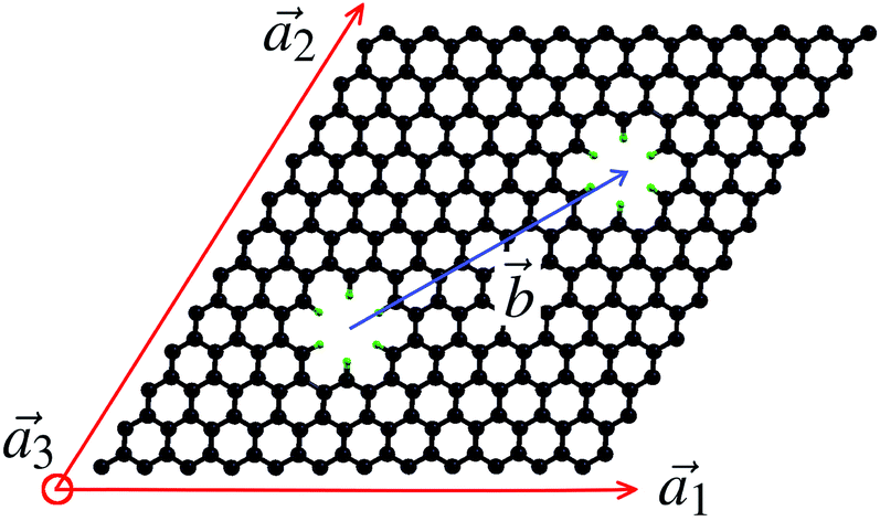 | ||
Fig. 1 Unit cell of a 12 × 12 × 1 HG structure, with  and and  chosen along a graphene sheet, while viewed along the third vector, chosen along a graphene sheet, while viewed along the third vector,  . The vector describes the relative position of the SD dipoles. . The vector describes the relative position of the SD dipoles. | ||
For the current study, we considered systems with the following in plane N1 × N2 multiples of a0: 6 × 6, 9 × 9 and 12 × 12. In order to study their structural stability, systems with two inner diameters for the hydrogen passivated pores were considered: denoted by S (for “small”), where 6 carbon atoms which are nearest to the screw axis are replaced by hydrogens, and L (for “large”), where 18 carbon atoms are removed and 12H are added. Depending on the pore size, the system will be labeled as HG, for the pristine helical graphite, SS if both pores are small, SL for a combination of small and large pores, and LL when both pores are large. The vectors for the three system sizes were chosen as (4, 2), (6, 3) and (7, 4) (in graphene lattice units a0). Furthermore, hybrid structures based on alternating regions of carbon and boron nitride, a wide band gap semiconductor, were also investigated, as depicted in Fig. 2. In this case, the highly conductive regions are isolated from each other, leading to a guided current flow along the carbon spirals.
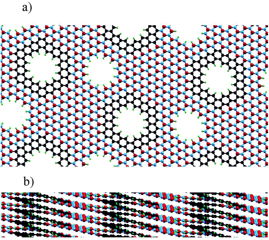 | ||
| Fig. 2 A typical HG structure with pores (12 × 12 LL–HG), made of hybrid graphene–boron nitride sheets: (a) top view of a single layer; (b) side view, showing the spirals in cross-section. | ||
The issue of structural stability is paramount for the mere existence of such metamaterials. First, the equilibrium configurations are obtained by structural relaxations, minimizing the total forces. This, however, does not ensure the intrinsic stability of the systems. An important stability criterion is to calculate and test the phonon spectrum against negative eigenvalues of the dynamical matrix. It must be stressed that, although numerous studies seem to rely solely on such a result in order to infer the stability of some atomic systems, such a validation is not sufficient and only indicates that the structure is stable against rather weak periodic lattice distortions. In order to give a stronger assessment regarding the stability of a newly proposed material, one must also find the minimum energy paths, i.e. saddle points, connecting adjacent local energy minima of the structural configuration space, e.g. using the nudged elastic bands technique.
Another important aspect is the presence of defects, such as external surfaces (the case for any finite system) or other internal structural defects that are present in real crystals. Any such symmetry breaking element could bring a system of this type out of a state of local minimum energy by collapsing the helices into the more energetically favorable stacked planar configuration.
As indicated in Fig. 3(a), the phonon spectra for pristine 6 × 6 HG system shows negative eigenvalues for all three acoustic and for the lowest optical branch. This directly indicates a system instability and the natural tendency of the spirals of opposite chirality to recombine, thus recovering the natural AB stacking. By contrast, considering the 6 × 6 SS–HG system, the phonon spectrum becomes entirely positive in Fig. 3(b). Further confirmation is found in Fig. 4(a), where the transition energy ΔEt, from a given configuration to the pristine AB stacked graphite, is plotted for several inter-spiral distances. With this approach we describe the recombination of adjacent SDs of opposite chirality by performing a bond-by-bond cut. The system shows a monotonic decrease in energy, as the two spirals are brought closer together which suggests that, even if the system resides in an energy minimum, any symmetry breaking along the  direction would cause it to collapse.
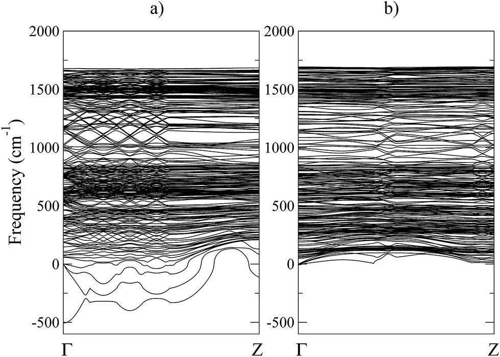 | ||
| Fig. 3 Phononic spectra showing the intrinsic instability (imaginary frequencies) of the pore-less, unpassivated 6 × 6 HG structure (a) in comparison with the 6 × 6 SS–HG system (b). | ||
 | ||
| Fig. 4 Energy differences ΔEt corresponding to transitions from a given meta-stable HG state to pristine AB graphite, for the three system sizes considered, with different pore diameters: (a) 6 × 6 SS–HG; (b) 9 × 9 SS–HG, SL–HG; (c) 12 × 12 SS–HG, SL–HG, LL–HG. Here, one SD is kept fixed, centered on one of the passivated pores, while the second one is displaced at neighboring sites along . The continuous lines indicate that the fixed helix is centered on the smaller pore while the dashed lines correspond to the cases when it is centered on the larger diameter pore. | ||
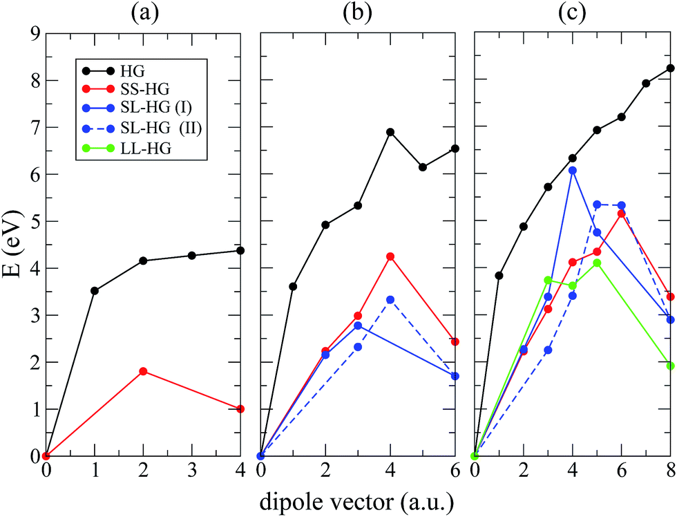
As a side note, it is somewhat surprising that in ref. 35 the authors suggest that a carbon allotrope with helical chains of opposite chirality, which could be described in our current notation as 3 × 3 cell (a1 = a2 = 3) and a dipole vector = (1,1), is dynamically stable. Since their conclusion is only drawn from an energy and phonon spectra investigation, a more detailed exploration of the energy landscape would be suggested.
A solution to stabilize the dipole in a HG crystal is to exploit the natural tendency of SDs to decrease internal stresses by introducing a hollow core.36,37 Such a configuration is also preferred because the hollow cores pin down each dislocation and prevent them from recombining. The 6 × 6 cell size allows only for small hollow cores to be considered, the 9 × 9 cell is large enough to introduce one small and one large hollow core, while in the 12 × 12 case, a pair of large hollow cores can be considered. In Fig. 4 the energy difference ΔEt = EAB − E is plotted, where EAB represents the energy of the graphite-like system, i.e. the corresponding system with or without pores, where the graphene sheets are stacked in AB configuration and E represents the system under consideration, that has one helix centered in one of the pores while the second one is placed in different intermediate positions between the two pores. The separation between the two helices is represented as the nth neighboring order of the lattice hexagon on which the second helix is centered on. One can see that maxima appear in ΔEt for all the cases where hollow cores are present: 6 × 6 – 0.8 eV (SS), 9 × 9 – 1.81 eV (SS) and 1.08 eV (SL), 12 × 12 – 1.76 eV (SS), 2.45 eV (SL), 2.18 eV (LL). In the SL configurations, moving the SD of the small pore or that of the large pore would not be symmetric. Although both of these cases were considered here, only the lowest saddle point obtained in the two calculations is indicated, i.e. the smallest energy difference that has to be overcome in order to transition from an HG configuration, corresponding to the highest separation between the helices, to the graphite-like AB configuration, when the helices have merged and have canceled out. We conclude that, if the pores are present in the system and if helices are centered on them, their recombination would correspond to overcoming a large enough energy barrier, i.e. the system is found in a metastable state. This indicates that it is thus possible to engineer a stable HG crystal. Additionally, Fig. 4 also shows that by increasing the distance between neighboring spirals the energy barrier between the helical configuration and the more stable AB graphite is enhanced.
3.2 Calculation of the current density and magnetic field
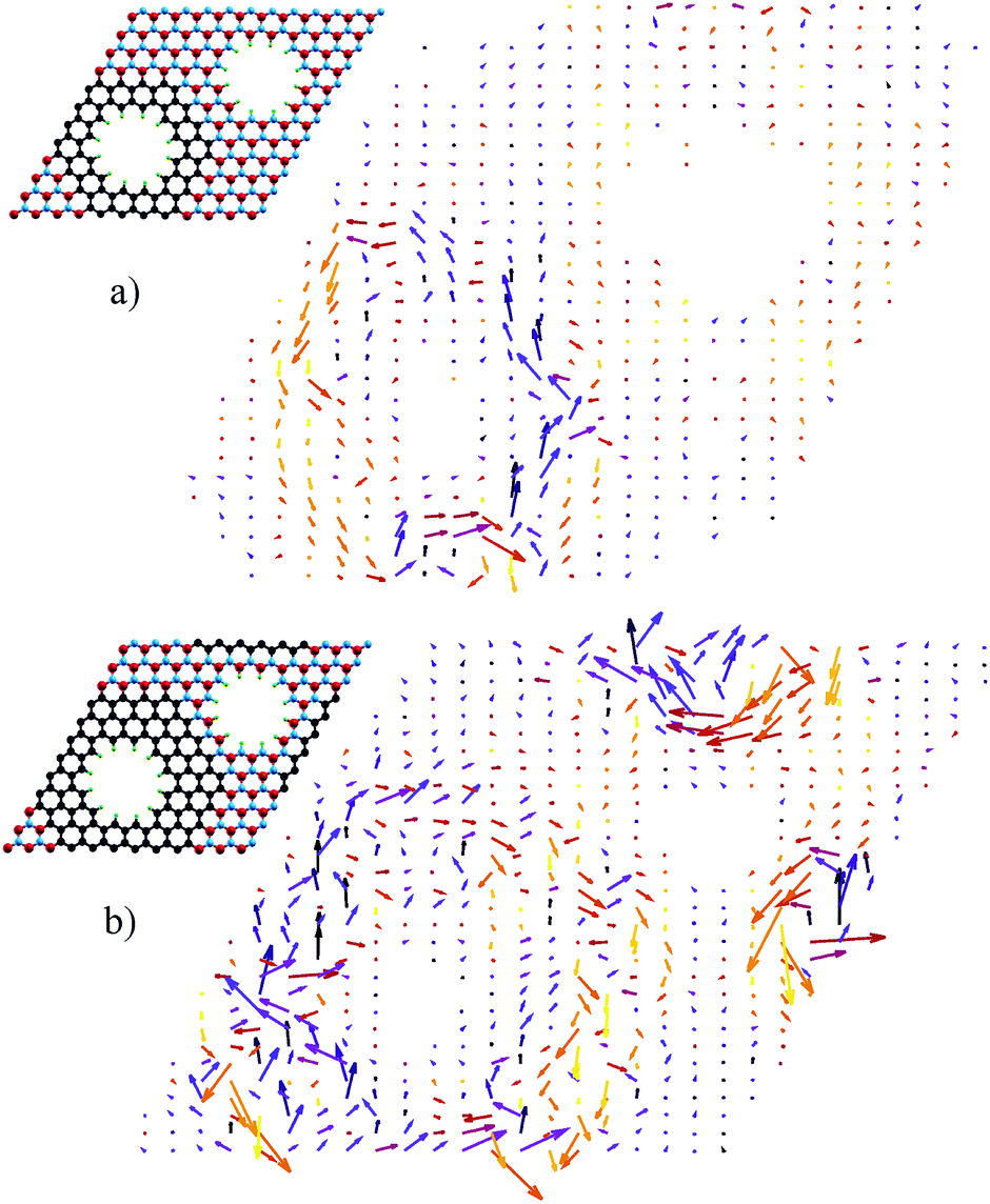
After performing structural relaxations and optimizations for stability, the electronic and transport properties were then analyzed for the three 12 × 12 systems (SS, SL and LL). It was found that all three are metallic, showing no bandgap. In order to determine the magnetic functionality of HG metamaterials, we first need to evaluate the charge current through the crystal structure under applied external bias. Since we are dealing with bulk systems, we calculate the current based on Bloch functions ΨE,k using the probability current operator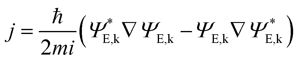 . In the coherent regime, in linear response, i.e. small applied bias U, and low for temperatures, the states contributing to the current are found in an energy interval around the Fermi energy EF, specified by −U/2 < EF < U/2, with U = 1 V. The integration over the reciprocal space is performed while only considering the E and k pairs for which the wavefunctions ΨE,k give rise to a positive current along the direction of transport, in this case, parallel to the axis of the SDs. The projection of the current density onto a section through the unit cell, perpendicular to the screw axes, is represented in Fig. 5 for three cases of a 12 × 12 system. Fig. 5 also shows that the current density vectors generally appear to be oriented from on side to the other of the cell and do not follow the winding SDs. This is not surprising since the current tends to flow along the distorted graphene sheet that makes up the HG structure rather than wind along the center of the helices.
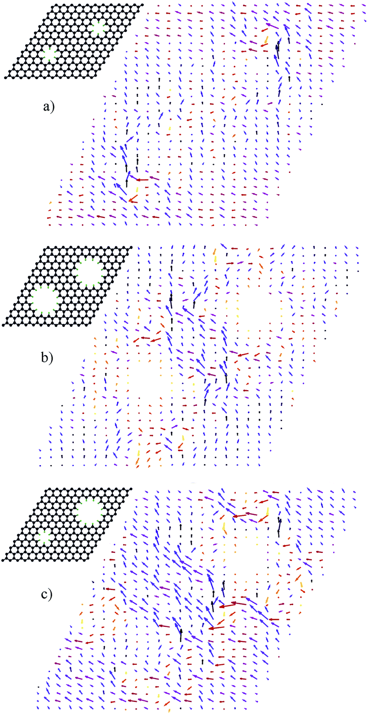 | ||
Fig. 5 Current distribution maps in cross-section calculated for U = 0.5 V: (a) SS, (b) SL and (c) LL systems. To a large extent, the current flow is not concentrating around the screw axis. For better visibility, the color scale indicates the angle orientation of the discretized current density projected on the ( ) plane, ranging from dark purple to yellow for angles within (0, π) interval. ) plane, ranging from dark purple to yellow for angles within (0, π) interval. | ||
The magnetic field ![[B with combining right harpoon above (vector)]](https://www.rsc.org/images/entities/i_char_0042_20d1.gif) is calculated at the center of the pores of each of the helices that make up a unit cell, by considering the contribution of the current inside a unit cell volume centered at each of the two locations. Effectively, this acts as a cut-off radius for the contribution of current that is considered and also treats each helix as an independent solenoid along the
is calculated at the center of the pores of each of the helices that make up a unit cell, by considering the contribution of the current inside a unit cell volume centered at each of the two locations. Effectively, this acts as a cut-off radius for the contribution of current that is considered and also treats each helix as an independent solenoid along the  axis. The magnetic field is thus computed by using the Biot–Savart law,
 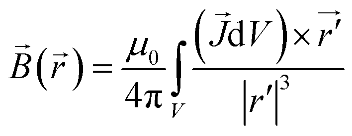 , and by integrating over the current density in a unit cell of volume V. Taking into account the geometry of the unit cell, i.e. a3/a1 ∼ 10, this value can be interpreted as the magnetic field produced by a current loop centered at either axes of the helices. Now we determine along each of the two screw/solenoid axes for systems of infinite length. This is useful when comparing the field values to the ones indicated in previous papers.13,21,22 In order to do this, we simplify the problem at hand by approximating the magnetic field previously computed as one produced by a current loop with radius 1 nm, i.e.
 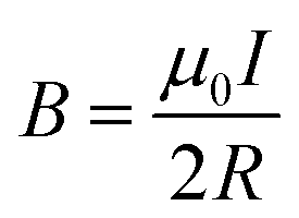 . For an infinite solenoid, the magnetic field is B = μ0nI, where n represents the number of turns of a solenoid per unit length, here n = 1/a3. Based on these approximations, it is possible to give an estimation for the intensity of the magnetic field along the core of the SDs, as shown in Fig. 6.
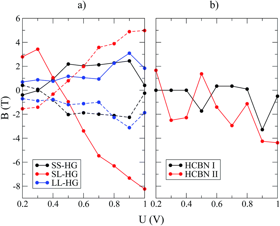 | ||
Fig. 6 Magnetic field projection on the  axis in the HG structures based on carbon (a) and on hybrid carbon–boron nitride (b) systems. The continuous and dotted lines indicate the field computed for the two distinct pores of a unit cell. For the asymmetric SL case, the continuous line indicates the magnetic field values for the smaller pore, while the dashed line corresponds to the larger diameter pore. axis in the HG structures based on carbon (a) and on hybrid carbon–boron nitride (b) systems. The continuous and dotted lines indicate the field computed for the two distinct pores of a unit cell. For the asymmetric SL case, the continuous line indicates the magnetic field values for the smaller pore, while the dashed line corresponds to the larger diameter pore. | ||
Because of the small inner diameter of the hollow core and the metallic behavior demonstrated by the HG systems, intense magnetic fields, of the order of several Tesla, can appear in the bulk of the metamaterial, which is the same order of magnitude as those reported for one dimensional systems.13,21 Interestingly, the magnetic field intensity does not depend monotonously on the applied bias, but rather oscillates and even reverses its sign, as indicated in Fig. 6. It can also be seen (Fig. 6) that for both symmetric systems (SS and LL) the magnetic field intensity along one screw axis is almost perfectly matched along the other. In spite of relatively high values, the orientation of the local magnetic field does not correspond to individual current loops and the overall effect is not that one would expect from an ideal solenoid. Rather, as can be seen in Fig. 5, in all three cases, the current will flow mostly along the central ramps that the spirals form in each cell.
Such an effect is not desirable since the material will just act as a bulk conductor and will not generate the desired uniform magnetic field oriented along the direction of the chiral axis. A feasible solution would require that only helices with one of the two chiralities would produce magnetic field and, furthermore, that each must be electrically insulated from its neighbors in order to guide the current along the spiral. This can be accomplished by integrating the inner core of the carbon-based spirals into an insulating boron nitride matrix of similar geometry. Boron nitride is not only a good choice because of its large bandgap (∼5 eV), but it also structurally matches graphene and it has been proven that hexagonal carbon domains can be easily integrated in BN.38 Two geometries that match these requirements were chosen, as depicted in Fig. 7, with two different outer diameters for the carbon spiral but symmetric pores (LL). In the case of a smaller outer diameter CBN-I (Fig. 7(a)), a bandgap of ∼0.3 eV was found, while CBN-II (Fig. 7(b)) shows no bandgap.
 | ||
| Fig. 7 Current distribution maps in cross-section calculated for U = 0.5 V in the case of CBN structures with small outer diameter CBN-I (a) and large outer diameter CBN-II (b) of the carbon domain. Vortexes are clearly observed around the screw axis while being effectively insulated from their neighbors. | ||
In Fig. 7, it can be seen that, especially for the case of a larger carbon domain, the current vortexes are not perfectly symmetrical around their axes. This is caused by the fact that the system tries to comply to the AB stacking of graphite which leads to a slight tilt, as if the helix is experiencing shear along the  axis. This, in turn, affects the charge flow. In both cases, as depicted Fig. 7, the current appears to flow in a roughly spiraling path along the axis of the SD.
In a similar fashion to the HG systems, Fig. 6(b) shows the magnetic field along the axis for a solenoid of infinite length. Because of the decrease in the density of states at the Fermi level as BN regions are introduced, the current and, implicitly, the magnetic field will be reduced while the oscillating behavior is nevertheless maintained. We can compare the magnetic properties of such hybrid C–BN metamaterials with those of known permanent magnets, specifically rare-earth magnets, which typically show a saturation magnetization between 1 and 1.5 T.39,40 Again, by considering a unit cell of our system as a current loop with magnetic moment M = IS (where S is the surface of a disc with 1 nm radius), the flux density can be computed as 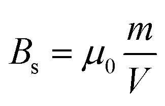 . For CBN II at U = 1 V, Bs = 11.2 T, which is roughly ten times the usual saturation remanence of rare-earth magnets. In this context, a simple calculation shows that only one conduction mode of fundamental conductance 2e2/h yields a current of 0.077 mA at an applied bias of 1 V, while the densely packed current loops in the spirals, with n ≈ 0.3 × 10¹⁰ m−1, produce a magnetic field of ∼0.3 T.
In order to better understand the complex oscillating behavior of the magnetic field represented in Fig. 6, a cross-section view of the current flow in the SL–HG and HCBN II systems is depicted in Fig. 8. The reason for the sign reversal of the magnetic field is immediately visible in Fig. 8 by observing the main flow of the current relative to the centers of the helices. In the case of SL–HG [Fig. 6(a)] one can see that the current flows around the outer edges of the two helices at 0.3 V (B = 3.4 T), while at 0.6 V (B = −3.3 T) the dominant flow is between them. A similar effect is visible in the case of HCBN II [Fig. 6(b))] where the main flow of the current reverses it's rotation relative to the center of the carbon helix. Although, intuitively, one might expect the current to follow the winding of the conductive helices, this is not necessarily the case when the graphene planes are distorted and, at the same time, when the inter-planar distances are relatively small. The propagating modes are energy dependent and, at finite bias, this can lead to currents of opposite chirality to that of underlying atomic helical structure.
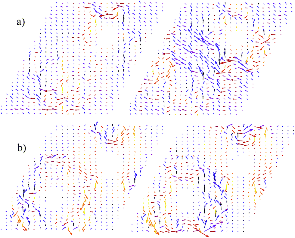 | ||
| Fig. 8 Current distribution maps in cross-section for: (a) SL–HG at 0.3 V, B = 3.4 T (left) and 0.6 V, B = −3.3 T (right) and (b) HCBN II at 0.2 V, B = 1.6 T (left) and 0.3 V, B = −2.5 T (right). In each case, the bias values were chosen for opposite orientations of the magnetic field, as indicated in Fig. 6. | ||
4 Conclusions
We investigated a novel metamaterial structure, which we call helical graphite, as a prototype material for producing intense magnetic fields. By employing DFT calculations, we provide a detailed discussion regarding the stability of the proposed systems and evaluate the charge transport and magnetic properties of such metamaterials under external bias. While pristine HG has shown the promising results by producing large internal magnetic fields, optimized structures based on a carbon–boron nitride hybrid are also indicated. The hybrid C–BN metamaterial shows the highest potential of producing intense magnetic fields, exceeding the values typically obtained in rare-earth magnets. In addition, since the metamaterial's construction allows the magnetic properties to be preserved over a range of scales, from individual helices and up to macroscopic systems, the HG structures may also find applications in the nanoscale control of magnetotransport based devices.Conflicts of interest
There are no conflicts to declare.Acknowledgements
This work was supported by the National Authority for Scientific Research and Innovation (ANCSI) under grant PN16420202 and Romania-JINR cooperation project JINR Order 220/10.04.2017, pp. 24.References
- W. Cai and V. Shalev, Optical Metamaterials – Fundamentals and Applications, Springer, 2010 Search PubMed.
- C. Caloz and T. Itoh, Electromagnetic metamaterials – Transmission Line Theory and Microwave Applications, John Wiley & Sons, 2006 Search PubMed.
- T. Han, X. Bai, J. T. L. Thong, B. Li and C.-W. Qiu, Adv. Mater., 2014, 26, 1731–1734 CrossRef CAS PubMed.
- B. Florijn, C. Coulais and M. van Hecke, Phys. Rev. Lett., 2014, 113, 175503 CrossRef PubMed.
- S. Xiao, U. K. Chettiar, A. V. Kildishev, V. Drachev, I. C. Khoo and V. M. Shalaev, Appl. Phys. Lett., 2009, 95, 033115 CrossRef.
- V. M. Shalaev, Nat. Photonics, 2007, 1, 41–48 CrossRef CAS.
- C. Sheng, H. Liu, Y. Wang, S. N. Zhu and D. A. Genov, Nat. Photonics, 2013, 7, 902–906 CrossRef CAS.
- S. Liu, W. Chen, J. Du, Z. Lin, S. T. Chui and C. T. Chan, Phys. Rev. Lett., 2008, 101, 157407 CrossRef PubMed.
- J. Jin, S. Liu, Z. Lin and S. T. Chui, Phys. Rev. B: Condens. Matter Mater. Phys., 2009, 80, 115101 CrossRef.
- S. Liu, W. Lu, Z. Lin and S. T. Chui, Phys. Rev. B: Condens. Matter Mater. Phys., 2011, 84, 045425 CrossRef.
- Z. Wang, Y. D. Chong, J. D. Joannopoulos and M. Soljačić, Phys. Rev. Lett., 2008, 100, 013905 CrossRef PubMed.
- J. Yu, H. Chen, Y. Wu and S. Liu, EPL, 2012, 100, 47007 CrossRef.
- F. Xu, H. Yu, A. Sadrzadeh and B. I. Yakobson, Nano Lett., 2016, 16, 34–39 CrossRef CAS PubMed.
- D. K. Berry, M. E. Caplan, C. J. Horowitz, G. Huber and A. S. Schneider, Phys. Rev. C, 2016, 94, 055801 CrossRef.
- M. Rickhaus, M. Mayor and M. Juricek, Chem. Soc. Rev., 2016, 45, 1542–1556 RSC.
- M. Terasaki, T. Shemesh, N. Kasthuri, R. Klemm, R. Schalek, K. Hayworth, A. Hand, M. Yankova, G. Huber, J. Lichtman, T. Rapoport and M. Kozlov, Cell, 2013, 154, 285–296 CrossRef CAS PubMed.
- L. Pauling, R. B. Corey and H. Branson, Proc. Natl. Acad. Sci. U. S. A., 1951, 37, 205–211 CrossRef CAS.
- J. Watson and F. Crick, Nature, 1953, 171, 737–738 CrossRef CAS PubMed.
- T. Korhonen and P. Koskinen, AIP Adv., 2014, 4, 127125 CrossRef.
- S. M. Avdoshenko, P. Koskinen, H. Sevinçli, A. A. Popov and C. G. Rocha, Sci. Rep., 2013, 3, 1632 CrossRef PubMed.
- Z.-Y. Zhang, C. Miao and W. Guo, Nanoscale, 2013, 5, 11902–11909 RSC.
- F. Xu, A. Sadrzadeh, Z. Xu and B. I. Yakobson, Comput. Mater. Sci., 2014, 83, 426–433 CrossRef CAS.
- A. Kuc and G. Seifert, Phys. Rev. B: Condens. Matter Mater. Phys., 2006, 74, 214104 CrossRef.
- I. Suarez-Martinez, G. Savini, G. Haffenden, J.-M. Campanera and M. I. Heggie, Phys. Status Solidi C, 2007, 4, 2958–2962 CrossRef CAS.
- G. R. Hennig, Science, 1965, 147, 733–734 CAS.
- A. R. Patel and O. P. Bahl, Br. J. Appl. Phys., 1965, 16, 169 CrossRef.
- J.-M. Leyssale, J.-P. D. Costa, C. Germain, P. Weisbecker and G. Vignoles, Carbon, 2012, 50, 4388–4400 CrossRef CAS.
- S. R. Kennedy, M. J. Brett, O. Toader and S. John, Nano Lett., 2002, 2, 59–62 CrossRef CAS.
- X. Xiao, T. E. Beechem, M. T. Brumbach, T. N. Lambert, D. J. Davis, J. R. Michael, C. M. Washburn, J. Wang, S. M. Brozik, D. R. Wheeler, D. B. Burckel and R. Polsky, ACS Nano, 2012, 6, 3573–3579 CrossRef CAS PubMed.
- J. M. Soler, E. Artacho, J. D. Gale, A. García, J. Junquera, P. Ordejón and D. Sánchez-Portal, J. Phys.: Condens. Matter, 2002, 14, 2745 CrossRef CAS.
- N. Ooi, A. Rairkar and J. B. Adams, Carbon, 2006, 44, 231–242 CrossRef CAS.
- D. M. Ceperley and B. J. Alder, Phys. Rev. Lett., 1980, 45, 566–569 CrossRef CAS.
- H. J. Monkhorst and J. D. Pack, Phys. Rev. B: Condens. Matter Mater. Phys., 1976, 13, 5188–5192 CrossRef.
- A. Kokalj, J. Mol. Graphics Modell., 1999, 17, 176–179 CrossRef CAS PubMed.
- J.-T. Wang, C. Chen, E. Wang and Y. Kawazoe, Sci. Rep., 2014, 4, 4339 CrossRef PubMed.
- J. P. Golightly, Z. Kristallogr. - Cryst. Mater., 1969, 310–313 CrossRef CAS.
- W. Si, M. Dudley, R. Glass, V. Tsvetkov and C. Carter, J. Electron. Mater., 1997, 26, 128–133 CrossRef CAS.
- Z. Liu, L. Ma, G. Shi, W. Zhou, Y. Gong, S. Lei, X. Yang, J. Zhang, J. Yu, K. P. Hackenberg, A. Babakhani, J.-C. Idrobo, R. Vajtai, J. Lou and P. M. Ajayan, Nat. Nanotechnol., 2013, 8, 119–124 CrossRef CAS PubMed.
- D. Jiles, Acta Mater., 2003, 51, 5907–5939 CrossRef CAS.
- E. Nesbit and J. Wernick, Rare earth permanent magnets, Academic Press, 1973 Search PubMed.
| This journal is © The Royal Society of Chemistry 2017 |