
 Open Access Article
 This Open Access Article is licensed under a
 Creative Commons Attribution 3.0 Unported Licence
N-Channel and P-channel few-layer InSe photoelectric devices†
Lin Tao and
Yongtao Li *
*
College of Material and Energy, Guangdong University of Technology, Guangzhou 510006, People's Republic of China. E-mail: liyt@semi.ac.cn
First published on 25th October 2017
Abstract
Herein, high-quality bulk InSe was grown by a low-cost pathway, after which mechanically exfoliated few-layer InSe nanosheets were obtained on a SiO2/Si substrate. The field-effect transistor (FET) devices with InSe channels were fabricated using two methods, including the shadow mask technique (SMT) and the ultraviolet lithography technique (ULT). Distinct different conducting characteristics were found in these devices on the basis of their manufacturing process, where the FET devices made by SMT displayed N-type channels, while P-type channels were obtained when ULT was used. Electrical and photoelectric properties studies demonstrated that the InSe devices made by SMT and ULT possess a high on/off ratio (4.7 × 10⁴ and 1.4 × 10²), mobility (18.7 cm2 V−1 s−1 and 0.33 cm2 V−1 s−1), photoresponsivity (0.59 A W−1 and 2.7 A W−1) and external quantum efficiency (115% and 527%), respectively. Theoretical and experimental investigation showed that the charge transfer between the H2O molecules and the InSe nanosheets caused the change in the conducting performances, and the defects led to an even heavier P-type doping effect in the channel.
Introduction
Since it was first discovered in 2004, graphene has attracted extensive attention due to its extremely high charge-carrier mobility,1,2 good optical transparency3 and flexibility.4 However, the nature of the zero band gap in graphene also seriously hinders its use as micro-/nano-electronic devices in electronic products. On the contrary, transition metal dichalcogenides (TMD) possess an adjustable band gap, great electrical and optical properties.5 The TMD monolayers (MX2) are a class of sandwich 2D materials with X atoms at the top and bottom and M atoms in between. Typically, M is a transition metal element from group IV, group V, or group VI, and X is a chalcogen (S, Se or Te). TMDs, such as MoS2 and SnS2, transistors have been theoretically and experimentally confirmed, and showed great potential as low-power, high-performance electronic devices for future applications.6–10 For example, the current on/off ratio of single-layer MoS2 transistors exceeds 108 at room temperature, which is much higher than that (approximately 100) of graphene transistors.6In recent years, layer-structure Indium selenide (InSe), belonging to III–V group compounds, has become one of the most attractive two-dimensional materials due to its excellent electronic and optoelectronic performance. Many efforts have been made in the investigation of its basic properties and for improving strategies for InSe. Feng et al. demonstrated high-performance multi-layer InSe transistors on a poly-(methyl methacrylate) (PMMA)/Al2O3 bilayer dielectric with a room-temperature mobility greater than 1000 cm2 V−1 s−1, and the transistors showed high current on/off ratios of 1 × 10⁸, revealing their great potential as field-effect transistor (FET) devices.11,12 Moreover, Lei et al. presented research showing that devices of mechanically exfoliated few-layer InSe flakes could be used as a photo sensor with a high photo-responsivity.13,14 The Zhang group have reported a theoretical study about charge transfer and functionalization of monolayer InSe by adsorption of different molecules, causing an effective doping effect to the InSe.15 Boukhvalov et al. also demonstrated that a BN coated InSe device possesses a bipolar characteristic while the uncapped one exhibited a P-doping property for the absorption.16 In spite of this, the techniques for effectively controlling the conducting channel of few-layer InSe devices still need further study, and the controllable and efficient strategy to achieve N-type and P-type channel InSe FETs is of great importance for its use in future electrical applications.
Here, large-size and high-quality bulk InSe was synthesized by a simple chemical vapor transport (CVT) method. Few-layer InSe nanosheets were also mechanically exfoliated onto a SiO2/Si substrate from the bulk material, and an atomic force microscope (AFM) demonstrated that the thickness of the sheets could be down to several nanometers. On this basis, two methods, including the shadow mask technique (SMT) and the ultraviolet lithography technique (ULT), have been employed to fabricate field-effect transistor devices using the few-layer InSe nanosheets as channels. The impressive results of the same batch of samples with different fabrication techniques showed that the FET devices made by SMT displayed N-type channels, while P-type channels were obtained when ULT was used. Studies on the electrical and photoelectric properties demonstrated that the InSe devices made by SMT and ULT possess a high on/off ratio (4.7 × 10⁴ and 1.4 × 10²), mobility (18.7 cm2 V−1 s−1 and 0.33 cm2 V−1 s−1), photoresponsivity (0.59 A W−1 and 2.7 A W−1) and external quantum efficiency (115% and 527%), respectively. Theoretical and experimental investigation showed that the charge transfer between H2O molecules and InSe nanosheets played a major role in the P-type doping behavior, and the defects (or vacancies) caused a heavier doping effect in the channel.
Results and discussion
Synthetic process of the bulk InSe material was conducted via a CVT technique, where pure In particles reacted with Se powder at a high temperature and formed layer-structure InSe blocks when cooled down slowly (see the detailed process in the Experimental section). As shown in Fig. 1a, the finished product of bulk InSe exhibits a color of darkish silver and the size of the material can also grow up to several millimeter in length and width. Thickness of the layered InSe was then reduced by the mechanical exfoliation method and then transferred to a clean SiO2/Si substrate for further characterization. There is a certain probability that few-layer or even monolayer InSe nanosheets could be obtained (Fig. 1b). Fig. 1c exhibits a typical optical image of a thin InSe nanosheet and our AFM measurement confirmed a thickness of about 4 nm of the sample (Fig. 1d). The lattice structure of layered InSe is also presented in Fig. 1e and f. In the case of the monolayer InSe, the Se atoms are located at the top and bottom of the layer, while two layers of In atoms are located in the middle, where the atoms connect to surrounding ones via chemical bonds. While few-layer or bulk InSe are composed of vertically stacked monolayer ones by van der Waals interaction, with a layer spacing of about 0.8475 nm.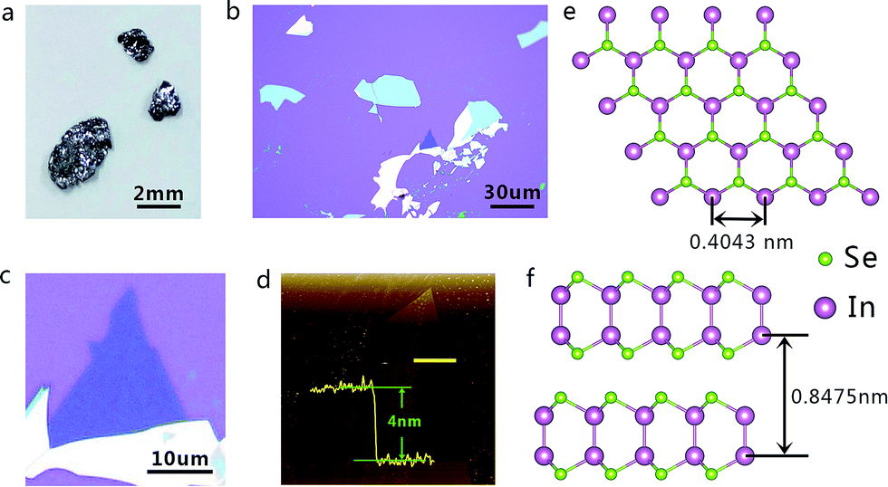 | ||
| Fig. 1 (a) Image of bulk InSe. (b) Low-magnification optical image of mechanically exfoliated multi-layer and few-layer InSe sheets on SiO2/Si substrate. (c) High-magnification optical image of few-layer InSe nanosheet. (d) AFM image and height profile of the InSe nanosheet in (c). (e) The top view and (f) side view of InSe lattice structure. | ||
Raman measurement was also employed to characterize the layered material. As shown in Fig. 2, the Raman spectrum collected from a few-layer InSe nanosheet revealed intensity peaks at about 116.2 cm−1, 177.4 cm−1 and 227.48 cm−1, corresponding to the A11g, E12g and A21g mode in the InSe, respectively. Moreover, no obvious shift of the Raman peaks were found in the bulk and few-layer InSe, except that intensity of the peaks were stronger in the bulk than in the few-layer nanosheets. On the other hand, the PL spectroscopy, which provided us with an effective way to gain the band gap width information of semiconductors, was also used in our experiments (Fig. S1†). The positions of the PL peaks of InSe nanosheets demonstrated an obvious trend of redshift as the thickness was increased from several layers to bulk. We transferred the nanosheets onto a Cu grid and performed TEM and electron diffraction studies to gain fine lattice information about the sample. The selected area electron diffraction (SAED) pattern taken from the sheet displayed a typical six-fold symmetry, whose set of hexagonal diffraction spots could be indexed to the (001) surface of the InSe lattice (Fig. S2†). SAED patterns at different positions on the nanosheet had this common feature with the same orientation, revealing the nature of a single crystal of our sample. The systematic characterizations described above demonstrated the high quality of the InSe nanosheets used in our experiment, which was an important basis for our further investigation about interesting electrical and photoelectrical properties of this semiconductor.
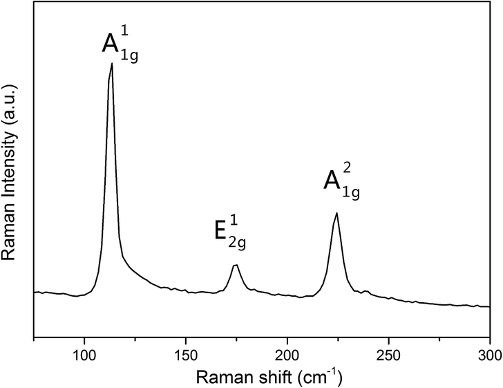 | ||
| Fig. 2 Raman spectrum of a few-layer InSe nanosheet. | ||
To evaluate the electrical and photoelectrical properties of the InSe nanosheets, few-layer samples on SiO2/Si substrate were then fabricated into FET devices via two different methods, namely the SMT and ULT. In the SMT process (Fig. 3a), a major feature was that a gold ribbon was used as a mask, which could stop the gold atoms depositing onto the device channel while symmetric drain and source electrodes were utilized during the metal evaporating process. On the other hand, the ULT process (Fig. 3b) adopted standard semiconductor device technology in our experiment. Detailed procedures of these two methods are illustrated in the Experimental section.
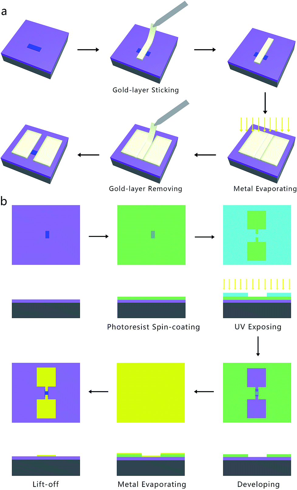 | ||
| Fig. 3 (a) Shadow mask technique used for the fabrication of FET devices. Gold ribbon was employed as the shadow mask to form the channel in FET. The asymmetric electrodes were utilized in the metal evaporating process, and the gold ribbon was removed by probe in the final step. (b) Ultraviolet lithography technique used for the fabrication of FET devices. The process adopted standard semiconductor device technology, including photoresist spin-coating, UV light exposure, developed by developer, goal thermal evaporating and the final lift-off procedure. | ||
Several points deserve to be mentioned here for a clear sense of these techniques. Firstly, no obvious differences could be observed in the final devices made by these two methods, except that the electrodes in the ULT FET possess regular shapes and sharper edges corresponding to the photomask, while the electrodes in the SMT devices might be less regular because of the manual operations in the procedure of transferring and pasting gold ribbons. The reliability of these two techniques have been verified by our group and many other groups in previous reports.17–20 Secondly, a large difference in these methods is that little or even no damage will be introduced into or onto the surface of the sample in the SMT devices because the gold ribbon was only slightly covering the channel area of the nanosheet while there was not any chemical reaction occurring in the whole process. However, in the fabrication process of ULT devices, some chemical substances, such as photoresist, strong alkaline developer, deionized H2O, and acetone were employed. As a result, materials such as organic semiconductors, substances susceptible to alkali corrosion, etc., may be affected and exhibit some interesting properties.
We then probed the devices with respect to their electrical and photoelectrical properties under natural air environment at room temperature. The schematic and optical image of the few-layer InSe FET device fabricated by SMT is shown in Fig. 4a, where the InSe nanosheet served as a conducting channel with a size of 12 um in length and 10 um in width. Each end of the nanosheet was covered by a gold film as the drain and source electrode, and the N-doped SiO2/Si substrate was used as a bottom gate to adjust the carriers in the channel. As shown in Fig. 4c, the transfer curve demonstrated a typical N-type conducting characteristic of the channel, and the current on/off ratio was able to exceed 4.7 × 10⁴, and the off state of the drain-source current (Ids) was about 1.0 × 10⁻¹⁰ A under a field effect of −80 V. Moreover, mobility of the InSe nanosheet can also be extracted from the transfer curve following the equation: 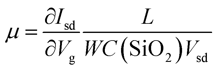 , where W is the InSe nanosheet FET channel width of 10 um, L is the FET channel length of 12 nm, and C(SiO2) = 11.6 nF cm−1 is the capacitance of the 300 nm SiO2 layer. The calculated mobility of the device is 18.7 cm2 V−1 s−1. The output curves were obtained by measuring the Vsd from −1 V to 1 V at a Vg of −80 V and then increased to Vg to 80 V gradually repeating above this step (Fig. 4d). The obvious change of the Ids under different gate voltage effects indicated the effective adjustment of the electric field on the conducting performance of the InSe channel.
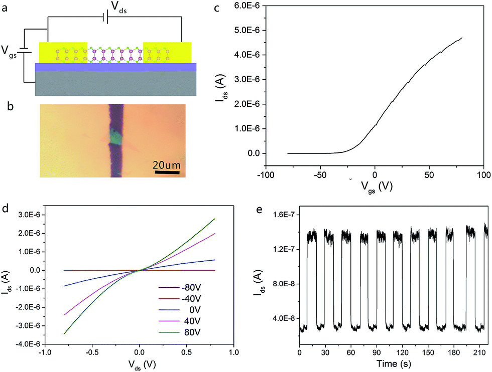 | ||
| Fig. 4 (a) Schematic and (b) optical image of InSe FET device fabricated by SMT. (c) Room-temperature transfer characteristic of the FET under a bias voltage of 1 V. (d) Ids–Vds characteristics of the device under different gate voltages in dark condition. (e) Time-resolved Isd of the InSe photodetector in response to light (635 nm laser, 0.2 W cm−2) on and off states under a bias voltage of 1 V. | ||
Fig. 4e is the time-dependent Isd of the InSe nanosheets with the laser switching between the on and off states under a source-drain voltage of 1 V. The curve shows that the ratio of the light current (Ilight) and dark current (Idark) is 4.4 (Vsd = 1 V) with a light current of about 1.34 × 10⁻⁷ A and a dark current of 3.03 × 10⁻⁸ A. In addition, the photoresponsivity R could be calculated by using the formula  , where Iph is a photocurrent defined as Iph = Ilight − Idark and P is the light power and S = 120 μm2. The external quantum efficiency (EQE) could be calculated by using the equation
  where h is Planck's constant (6.62 × 10⁻³⁴); c is the velocity of light (3 × 10⁸); e is the electron charge (1.6 × 10⁻¹⁹); and λ is the excitation wavelength. In this work, we chose a wavelength of 638 nm and a 0.2 W cm−2 laser to illuminate. The calculated response of the photoresponsivity R and the EQE of the InSe nanosheets are 0.59 A W−1 and 115%, respectively.
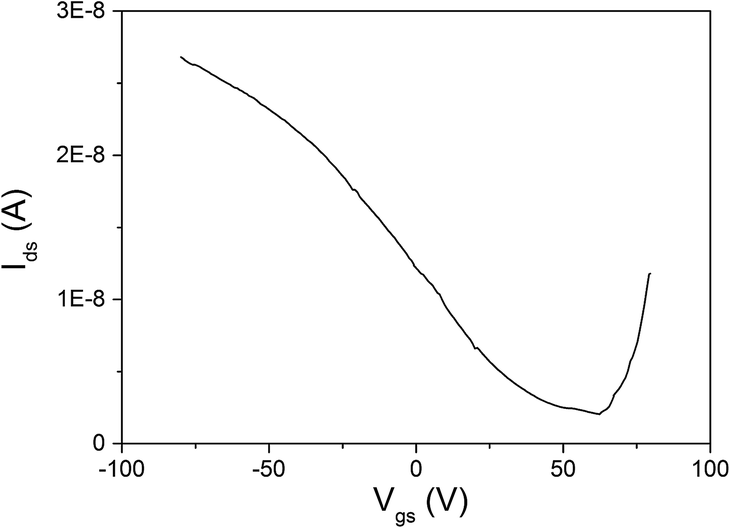
Considering the features of the InSe FET device fabricated by ULT, a distinct change in the conducting type of the channel was observed, and the devices exhibited a typical P-type conducting characteristic of the channel. Fig. 5a presents the model and image of the device made via ULT. In general, the structure of the ULT device was the same as that made by SMT. Interestingly, the transfer curve in Fig. 5b presented a P-type channel in the device, where the drain-source current was at a minimum under gate voltage of 80 V while it increased monotonously to the largest current under a gate voltage of −80 V. The current on/off ratio was about 140 with a maximum current of 3.66 × 10⁻⁷ A and minimum current of 2.6 × 10⁻⁹ A at −80 V and 80 V, respectively. Mobility of the P-type channel was extracted to be 0.33 cm2 V−1 s−1.
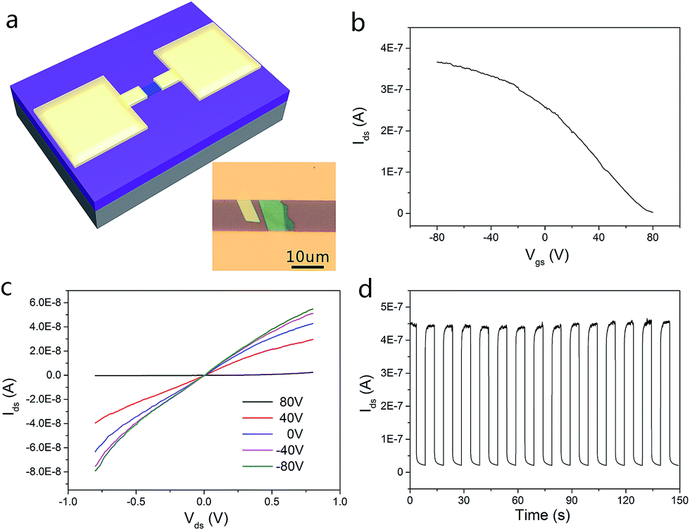 | ||
| Fig. 5 (a) Model and optical image of the InSe FET device fabricated by ULT. Sharper edges of electrode can be obtained in this method in comparison to that made in SMT. (b) Room-temperature transfer characteristic of the FET under a bias voltage of 1 V. (c) Ids–Vds characteristics of the device under different gate voltages in dark conditions. (d) Time-resolved Isd of the InSe photodetector in response to light (635 nm laser, 0.2 W cm−2) on and off states under a bias voltage of 1 V. | ||
Fig. 5c also displays the output curves of the device under different gate voltages, and the change of the Ids possessed an opposite trend in comparison to that in the SMT device (Fig. 4c). Furthermore, the InSe FET made by ULT also demonstrated good photoelectrical properties when being exposed to illumination (Fig. 5d). The Ilight/Idark ratio was about 18 with a light current of 4.4 × 10⁻⁷ A and a dark current of 2.4 × 10⁻⁸ A. The photoresponsivity R and EQE of the device were also extracted to be 2.7 A W−1 and 527%, respectively. The table of physical properties of the InSe devices fabricated by SMT and ULT can also be seen in Table 1.
| InSe (SMT) | InSe (ULT) | |
|---|---|---|
| Conduction type | N type | P type |
| Mobility (cm2 V−1 s−1) | 18.7 | 0.33 |
| On/off ratio | 4.7 × 10⁴ | 1.4 × 10² |
| Photoresponsivity (A W−1) | 0.59 | 2.7 |
| External quantum efficiency | 115% | 527% |
This study provides us an with important lesson that we are able to controllably acquire N-type and P-type channel few-layer InSe FET devices by the means of using different fabrication methods, namely SMT and ULT. Additionally, the feature of N-type characteristic in the SMT-made InSe devices are also consistent with that demonstrated in previous reports.11,12 After comparing the detailed process in these two techniques carefully, the impact of H2O adsorption was believed to be the major fact that caused the P-type changing in the few-layer InSe nanosheets. As we have mentioned above, strong alkaline developer solution and deionized H2O have been employed during the fabrication process in ULT (further details in the Experimental section). The adsorption energies of H2O on the InSe nanosheet was theoretically calculated via a first-principle calculation method and was extracted from the formula: ΔE = Etotal − EInSe − EH2O, and a calculation result of −0.23 eV was obtained, demonstrating that the H2O molecules tended to adsorb on the surface of InSe. The adsorption of H2O caused electrons in the nanosheets to transfer to the H2O molecules for the stronger electronegativity of the oxygen atom in H2O (Fig. 6). The similar doping effect of H2O molecules on InSe has also been theoretically proven by Politano, where the adsorbed water molecules would attract electrons from their InSe substrate, causing a P-type doping in the channel.15,16 To further confirm the surface modification effect of water on InSe, the photolithographic-pattern transfer technique was also employed in our experiment, where the electrode patterns were transferred directly wetted onto the channel material (Fig. S3†), an interesting result was found that these devices demonstrated a typical bipolar behavior (Fig. 7).21 A similar performance was also found in the dry MST devices which had been soaked in deionized water for an hour. The above experimental and theoretical results gave us a hint that the water adsorption was one of the major factors that caused P-type doping in InSe, but some other factors might also promote the doping effect, because the devices made by ULT performed monotonously by P-channel in their transfer characteristics (Fig. 5b).
 | ||
| Fig. 6 The schematic of charge density difference between pristine InSe and H2O-adsorbed InSe monolayer. The yellow region denotes charge accumulation and the blue region denotes charge depletion. | ||
 | ||
| Fig. 7 Transfer characteristic of InSe device fabricated by photolithographic-pattern transfer technique. An obvious bipolar behavior can be seen in the result. | ||
Besides the H2O adsorption, another important chemical reagent, namely strong alkaline developer solution, was believed to be the major difference between the ULT process and other methods. Even though no noteworthy change could be observed in the InSe nanosheets before and after being fabricated into devices by ULT, the individual procedure of development by alkaline developer was studied separately to better understand its impact on the InSe. The developing time often needed 30 s in the real process, but a much longer time was tried in the control experiment to gain a more obvious outcome. As shown in Fig. 8, it was interesting to find that when the InSe nanosheets were soaked in the developer for half an hour, an evident appearance of etching was observed. In addition, all of the samples were etched away within an hour. This result reflects the knowledge that multiple In- and Se-vacancies can be caused on the surface of InSe nanosheets during the developing procedure even though the real developing time was only 30 s. In this way, the stronger activated energy at defects (In- and Se-vacancies) greatly help to promote the adsorption of H2O molecules, resulting in a heavier P-type doping in the devices fabricated by ULT.22 At the same time, the impact of the scattering centers (including H2O adsorption and defects) could also account for the relatively poorer mobility and on/off ratio in the ULT devices.
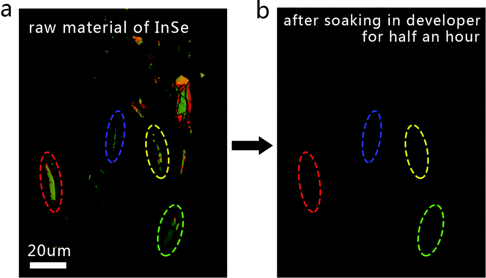 | ||
| Fig. 8 Optical images of multi-layer and few-layer InSe nanosheets (a) before and (b) after being etched by developer. | ||
Conclusions
In summary, we successfully developed a controllable strategy for the fabrication of N-channel and P-channel few-layer InSe FET devices. Electric and photoelectric property studies demonstrated that the MST FET possess a higher on/off ratio and mobility while the photoresponsivity and EQE were better in ULT devices. The SMT and ULT FET possess the following characteristics, on/off ratio (4.7 × 10⁴ and 1.4 × 10²), mobility (18.7 cm2 V−1 s−1 and 0.33 cm2 V−1 s−1), photoresponsivity (0.59 A W−1 and 2.7 A W−1) and external quantum efficiency (115% and 527%), respectively. Theoretical and experimental investigation showed that the charge transfer between H2O molecules and InSe nanosheets caused the P-type doping in InSe and the defects even strengthened the doping effect. These interesting findings in few-layer InSe devices could help to extend their use in high-performance FET, photodetectors and optoelectronic circuits.Experimental section
Synthesis of bulk InSe and preparation of few-layer InSe nanosheets
The synthesis of the bulk InSe crystal was performed by a CVT method in a horizontal single-zone tube furnace. Prior to the crystal growth, a quartz tube with the source materials was evacuated to below 10−5 Torr and securely sealed. The purity of the source materials was indium particles 99.99%, selenide powder 99.99%, with a molar ratio of In![[thin space (1/6-em)]](https://www.rsc.org/images/entities/char_2009.gif) :Se equal to 52:48. Next, the precursor was heated up to 685 °C at a rate of 1 °C min−1 and maintained for 10 hours to ensure sufficient diffusion and equilibration for the single-crystal synthesis. Furthermore, the temperature was increased to 700 °C and held in this condition over 3 hours to form a uniform InSe melt. The melt was then cooled down to 400 °C at a ramp rate of 20 °C per hour, followed by natural cooling to room temperature to obtain InSe crystals. The CVT growth yielded large-size and high-quality InSe single crystals.
:Se equal to 52:48. Next, the precursor was heated up to 685 °C at a rate of 1 °C min−1 and maintained for 10 hours to ensure sufficient diffusion and equilibration for the single-crystal synthesis. Furthermore, the temperature was increased to 700 °C and held in this condition over 3 hours to form a uniform InSe melt. The melt was then cooled down to 400 °C at a ramp rate of 20 °C per hour, followed by natural cooling to room temperature to obtain InSe crystals. The CVT growth yielded large-size and high-quality InSe single crystals.
Few-layer InSe nanosheets were exfoliated from the above-mentioned bulk crystals using scotch-tape micromechanical cleavage technique.23 Silicon chips with 300 nm SiO2 layer were used as substrates for a better visibility in the optical microscope image.
Transfer process for TEM characterization
The InSe nanosheets were transferred by a wet-transfer method. First, poly(methyl methacrylate) (PMMA) was spin-coated onto the substrate and baked on a heating plate at 150 °C for 30 min. After that, the substrate with PMMA was soaked in NaOH solution until the PMMA film with nanosheets separated from the substrate and floated on the solution surface. The PMMA film was rinsed with deionized water several times and transferred onto a TEM grid and dried. Finally, the PMMA film was dissolved in acetone for 30 min.Fabrication of devices by SMT
First, a gold layer with a thickness of about 100 nm was deposited onto a clean SiO2/Si wafer by thermal evaporation. The gold film was then scraped and separated into many gold ribbons (about 10 × 300 um) with the help of a probe in a probe station. In the second step, the gold ribbon was peeled off from the substrate using the probe under the effects of electrostatic interaction, and transferred onto another substrate covered with a few-layer InSe nanosheet, careful operations were conducted with the help of microscope so that the gold ribbon strode over the middle of the nanosheet. Then a pair of Au electrodes with a thickness of 30 nm were deposited onto the substrate by thermal evaporation. And edges of the silicon chips were covered with tin foil in case of connection between the electrodes and the side-face of the SiO2/Si substrate. Finally, by slightly removing the gold ribbon from the substrate by probe again, a channel in the device was accomplished.Fabrication of devices by ultraviolet lithography technique
The SiO2/Si substrate a with few-layer InSe on was first spin-coated with a thin layer of photoresist (AR-P 5350 of ALLRESIST GmbH Company) at 4000 rpm and then baked on a 100 °C heating plate for 4 minutes. After that, exposure was performed, in which a lithography mask was pressed onto the substrate, following exposing under UV light for 2 s. 0.8% tetramethylammonium hydroxide (TMAH) in deionized water was used as the development solution and the chip was dipped into the TMAH solution for 30 s in order to remove the photoresist in the exposure area. After that, a 30 nm Au layer was deposited onto the chip, followed by removing of the redundant Au layer and photoresist in acetone, and leaving the final electrodes contacting both ends of the few-layer InSe nanosheet.Etching of multi-layer and few-layer InSe sheets
The investigation into the InSe etching was conducted by soaking the sheets in alkaline developer for a certain time. Before the etching process, InSe sheets were firstly mechanically exfoliated onto SiO2/Si substrate and then a film of PMMA was spin-coated onto the substrate and baked at 150 °C for half an hour. The use of PMMA in this experiment was to stick the InSe sheets on the PMMA so that the sheets would not move away during the etching process. Microscope images were taken for comparison with the etched sheets later. The substrate covered by PMMA was then soaked in the developer, which was used in our ULT process, for a certain time from 10 min to one hour. At this time, the SiO2 layer would be etched first by the alkaline developer, so that the solution could get into the interlayer between the PMMA film and substrate. After a certain time, the substrate and PMMA were washed several times by deionized water and observed using a microscope.Characterization
The samples were characterized by optical microscopy, Raman spectroscopy (LabRAM HR 800, with laser excitation of 632 nm and a spot size of 1 μm), and TEM (Hitachi HT7700, 120 kV acceleration voltage). The devices were measured in natural air atmosphere at room temperature using an Agilent B2902A system. The mobility of the charge carriers is extracted from the equation: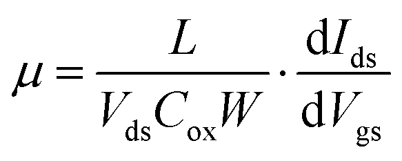 , where L and W are the device channel length and width, Ids and Vds are the current and voltage between source and drain electrodes, respectively, and Cox is the gate capacitance per unit area.
Conflicts of interest
There are no conflicts to declare.Acknowledgements
This work was financially supported by the National Natural Science Foundation of China (Grant No. 11674310, Grant No. 51602065 and Grant No. 61704034), and “Hundred Talents Program” of Guangdong University of Technology.Notes and references
- K. S. Novoselov, A. K. Geim, S. V. Morozov, D. Jiang, Y. Zhang, S. V. Dubonos, I. V. Grigorieva and A. A. Firsov, science, 2004, 306, 666–669 CrossRef CAS PubMed.
- Q. Liu, Y. Gong, T. Wang, W. L. Chan and J. Wu, Carbon, 2016, 96, 203–211 CrossRef CAS.
- S. Bae, H. Kim, Y. Lee, X. Xu, J. S. Park, Y. Zheng, J. Balakrishnan, T. Lei, H. R. Kim and Y. I. Song, Nat. Nanotechnol., 2010, 5, 574 CrossRef CAS PubMed.
- C. Yan, J. H. Cho and J. H. Ahn, Nanoscale, 2012, 4, 4870–4882 RSC.
- Y. Shi, H. Li and L.-J. Li, Chem. Soc. Rev., 2015, 44, 2744–2756 RSC.
- B. Radisavljevic, A. Radenovic, J. Brivio, V. Giacometti and A. Kis, Nat. Nanotechnol., 2011, 6, 147–150 CrossRef CAS PubMed.
- Z. Yin, H. Li, H. Li, L. Jiang, Y. Shi, Y. Sun, G. Lu, Q. Zhang, X. Chen and H. Zhang, ACS Nano, 2011, 6, 74–80 CrossRef PubMed.
- B. Radisavljevic, M. B. Whitwick and A. Kis, ACS Nano, 2011, 5, 9934–9938 CrossRef CAS PubMed.
- H. Song, S. Li, L. Gao, Y. Xu, K. Ueno, J. Tang, Y. Cheng and K. Tsukagoshi, Nanoscale, 2013, 5, 9666–9670 RSC.
- Q. Liu, B. Cook, M. Gong, Y. Gong, E. Dan, M. Casper, A. Stramel and J. Wu, ACS Appl. Mater. Interfaces, 2017, 9, 12728 CAS.
- W. Feng, W. Zheng, W. Cao and P. Hu, Adv. Mater., 2014, 26, 6587–6593 CrossRef CAS PubMed.
- S. Sucharitakul, N. J. Goble, U. R. Kumar, R. Sankar, Z. A. Bogorad, F.-C. Chou, Y.-T. Chen and X. P. Gao, Nano Lett., 2015, 15, 3815–3819 CrossRef CAS PubMed.
- S. Lei, L. Ge, S. Najmaei, A. George, R. Kappera, J. Lou, M. Chhowalla, H. Yamaguchi, G. Gupta and R. Vajtai, ACS Nano, 2014, 8, 1263–1272 CrossRef CAS PubMed.
- S. R. Tamalampudi, Y.-Y. Lu, U. R. Kumar, R. Sankar, C.-D. Liao, B. K. Moorthy, C.-H. Cheng, F. C. Chou and Y.-T. Chen, Nano Lett., 2014, 14, 2800–2806 CrossRef CAS PubMed.
- Y. Cai, G. Zhang and Y.-W. Zhang, J. Phys. Chem. C, 2017, 121, 10182–10193 CAS.
- A. Politano, G. Chiarello, R. Samnakay, G. Liu, B. Gürbulak, S. Duman, A. Balandin and D. Boukhvalov, Nanoscale, 2016, 8, 8474–8479 RSC.
- L. Jiang, J. Gao, E. Wang, H. Li, Z. Wang, W. Hu and L. Jiang, Adv. Mater., 2008, 20, 2735–2740 CrossRef CAS PubMed.
- Q. Tang, L. Jiang, Y. Tong, H. Li, Y. Liu, Z. Wang, W. Hu, Y. Liu and D. Zhu, Nanoscale Res. Lett., 2008, 3, 395 CrossRef PubMed.
- L. Jiang, H. Dong, Q. Meng, J. Tan, W. Jiang, C. Xu, Z. Wang and W. Hu, Adv. Mater., 2012, 24, 694–698 CrossRef CAS PubMed.
- N. Huo, J. Kang, Z. Wei, S. S. Li, J. Li and S. H. Wei, Adv. Funct. Mater., 2015, 24, 7025–7031 CrossRef.
- Y. Li, L. Huang, M. Zhong, Z. Wei and J. Li, Adv. Mater. Technol., 2016, 1, 1600001 CrossRef.
- Y. Li, H. Le, L. Bo, X. Wang, Z. Zhou, J. Li and Z. Wei, ACS Nano, 2016, 10, 8938 CrossRef CAS PubMed.
- M. Yi and Z. Shen, J. Mater. Chem. A, 2015, 3, 11700–11715 CAS.
Footnote |
| † Electronic supplementary information (ESI) available. See DOI: 10.1039/c7ra10588f |
| This journal is © The Royal Society of Chemistry 2017 |