
 Open Access Article
 This Open Access Article is licensed under a Creative Commons Attribution-Non Commercial 3.0 Unported Licence
A stable, efficient textile-based flexible perovskite solar cell with improved washable and deployable capabilities for wearable device applications†
Jeun-Yan Lama,
Jung-Yao Chenb,
Ping-Chun Tsaia,
Yun-Ting Hsiehb,
Chu-Chen Chueh *b,
Shih-Huang Tung*a and
Wen-Chang Chen*ab
*b,
Shih-Huang Tung*a and
Wen-Chang Chen*ab
aInstitute of Polymer Science and Engineering, National Taiwan University, Taipei 10617, Taiwan. E-mail: shtung@ntu.edu.tw; chenwc@ntu.edu.tw
bDepartment of Chemical Engineering, National Taiwan University, Taipei 10617, Taiwan. E-mail: cchueh@ntu.edu.tw
First published on 27th November 2017
Abstract
Organic–inorganic hybrid perovskite solar cells (PVSC) have appeared as promising high power-per-weight power systems for wearable electronic devices. Herein, we utilized a low-temperature electrodeposited tin oxide (SnO2) electron-transporting layer (ETL) coupled with a thin PCBM ETL and a functional encapsulating layer to realize an efficient, stable textile-based flexible PVSC. We first demonstrated that an easily accessible elastomer can serve as an effective encapsulating material for the fabricated flexible PVSC, as exemplified by the largely improved ambient stability and waterproof properties. Furthermore, we established that the good adhesive properties generated by the elastomer can largely enrich the deployable capability of the completed device stack as evidenced by the effortless integration of a completed device stack onto a textile. As a result, a ∼15% textile-based flexible PVSC with improved ambient stability and washable capability was demonstrated. A proof-of-concept device was successfully integrated with other electronic devices on a unitary textile to serve as an efficient power supply system for wearable electronic devices. The findings revealed in this work can promote the future potential applications of PVSCs in wearable device applications.
Introduction
The rapid progress of human civilization has been accompanied with a large demand for energy. Therefore, the development of renewable clean energy has become an urgent issue for this generation. From the sustainable perspective, solar energy has emerged as the most promising candidate due to its almost inexhaustible access and high radiation energy. More importantly, it requires no extra fuels and produces few by-products when supplying power silently.Among the rapid tide of photovoltaic techniques, organic–inorganic hybrid halide perovskite materials with a formula of ABX3 (A = Cs+, CH3NH3+, or CH(NH2)2+; B = Sn2+ or Pb2+; X = Cl−, Br−, or I−) have recently attracted worldwide attention since they not only possess exceptional opto-physical properties but also own facile solution processability.1–7 Such appealing features have enabled them to be considered as the most transformative photovoltaic technology nowadays.7 Currently, the state-of-the-art power conversion efficiency (PCE) of the perovskite solar cells (PVSCs) on rigid glass substrates has reached over 22% despite its only few year's development.8
Generally, PVSCs can be divided into two types, n-i-p and p-i-n structures, according to the sequence of the employed charge-transporting layers (CTLs). The prototypal PVSC is based on a conventional n-i-p configuration as evolved from the mesoporous dye-sensitized solar cells (DSSCs), which consists of a transition metal oxide (TMO) scaffold serving as an electron-transporting layer (ETL) at device's bottom side. Originally, the TMO is mainly based on TiOx and requires elaborate preparation procedures involving high-temperature sintering.5,9–13 However, such sophisticated processes would imperceptibly increase the production costs and limit the substrate choice.14 Further, it impedes the widespread applications of the derived devices in the flexible and wearable electronics, for which polymeric substrates with low glass transition temperatures were usually employed.15 For this reason, versatile low-temperature procedures are developed for TiOx. One example is that Kim et al. have adopted the atomic layer deposition (ALD) technology to prepare a TiOx layer ETL at a reduced temperature to realize an efficient (PCE: >12%) flexible conventional PVSC with satisfactory mechanic stability under 1000 bending cycles for a bending radius of 10 mm.16
Meanwhile, other TMOs besides TiOx with low-temperature processed capability are continuously exploited in the past few years, such as ZnO, SnO2, Zn2SnO4, and BaSnO3.17–19 Among them, SnOx-based TMO has attracted the most research attention due to its much higher electron mobility than TiOx. Several groups have individually developed distinct synthetic processes to prepare SnOx-based films at reduced temperatures to facilitate their electron-transporting properties to realize efficient PVSCs.20,21 Recently, we have also utilized the electrochemical deposition technique to successfully prepare a high-quality SnO2 film at a low temperature below 100 °C to fabricate efficient conventional PVSCs.15 These aforementioned achievements in developing efficient low-temperature processed ETLs indeed promote the future applications of PVSCs as promising high power-per-weight energy source for unmanned aerial vehicles for environmental and industrial monitoring, rescue and emergency response, and tactical security applications.22
While the current state-of-the-art PCE of PVSC can rival the performance of traditional inorganic photovoltaic techniques, more research focuses in this field have been shifted to improve its long-term device stability. The perovskite materials have been documented to be susceptible to moisture, thermal, and intense illumination.23–27 In this regard, the encapsulation of PVSC will play a pivotal role to sustain its long-term stability for real operation. At present, barriers and ALD technologies are the most commonly methods used for device encapsulation. For the device fabricated on the regular rigid substrates, it is quite common to employ a thin glass cover slip to cover the completed device stack, followed by sealing with UV curable epoxy resin.28–30 However, the UV exposure procedure needs to be carefully controlled to avoid deteriorating the perovskite layer. As for the flexible devices, the encapsulation is more challenging. Thus far, utilizing membranes31,32 or ALD technology are considered as the most feasible approaches for encapsulating flexible PVSCs.29,30,33,34
In this study, extended from our previous work,15 we employed the electrodeposited SnO2 film onto a flexible substrate to fabricate a flexible PVSC. Surprisingly, it is revealed that the quality of the low-temperature electrodeposited SnO2 film on the flexible substrate is inferior to the case deposited on regular rigid substrate, attributed to the lower conductivity of ITO on the flexible substrate. Fortunately, this deficiency can be compensated by introducing an additional fullerene layer on top of SnO2 film, as a common strategy adopted in regular conventional PVSCs. Furthermore, we manifested that an easily accessible elastomer can effectively encapsulate the fabricated flexible PVSC, as exemplified by its largely improved ambient stability and waterproof property. More intriguingly, its respectable adhesive property can also facilitate the effortless integration of the completed device stack onto a textile substrate. As a result, a ∼15% textile-based flexible PVSC with improved ambient stability and washable capability was demonstrated. A proof-of-concept device was successfully integrated with other electronic devices on a unitary textile to serve as an efficient power supply system, demonstrating its promising potential for the wearable device applications.
Results and discussion
Recently, we have employed a low-temperature electrodeposited SnO2 film to serve as an efficient ETL to realize an efficient PVSC on regular rigid ITO substrate.15 Regarding its low-temperature manufacturing process, we continuously explored its efficacy in fabricating efficient flexible PVSCs. An ITO/polyethylene naphthalate (PEN) substrate was herein chose to compare with the regular rigid ITO/glass substrate. It has been acknowledged that the ITO/flexible substrates (like PEN, terephthalate (PET), and polyimide (PI))-based devices typically possess inferior performance compared to the rigid ITO/glass counterparts due to the brittle and unsatisfactory bendable nature of ITO.35Fig. 1 presents the high-resolution TEM (HR-TEM) image and selected area electron diffraction (SAED) of the prepared SnO2 film. As can be seen, the inset fast Fourier transform (FFT) pattern shows clear ring patterns associated with diffraction spots. It indicates the highly crystalline structures of SnO2 with random orientation, being consistent to the morphology observed in the HR-TEM image.
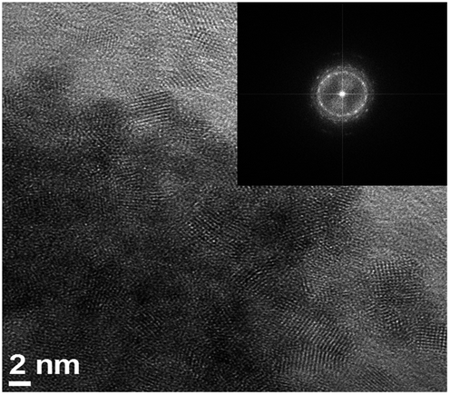 | ||
| Fig. 1 HRTEM micrograph of the electrodeposited SnO2 film with the corresponding insert FFT pattern. | ||
We first surprisingly observed that the quality of the electrodeposited SnO2 on the ITO/PEN substrate is much worse than the film deposited on the regular ITO/glass substrate. In contrast to the homogeneous surface morphology observed in the rigid substrate (Fig. S1†), the morphology of the SnO2 deposited on the ITO/PEN substrate is quite discrete and isolated island-like domains was clearly observed as shown in Fig. 2a. This discrepancy might originate from the lower conductivity of ITO on PEN than on glass since the brittleness of ITO might engender more defects existed in the substrate, which unavoidably leads to the less efficient electrodeposition of SnO2 film. Such incomplete surface coverage will also deteriorate the performance of its derived PVSC because the pin-hole formation could easily incur the shunting paths in the device.
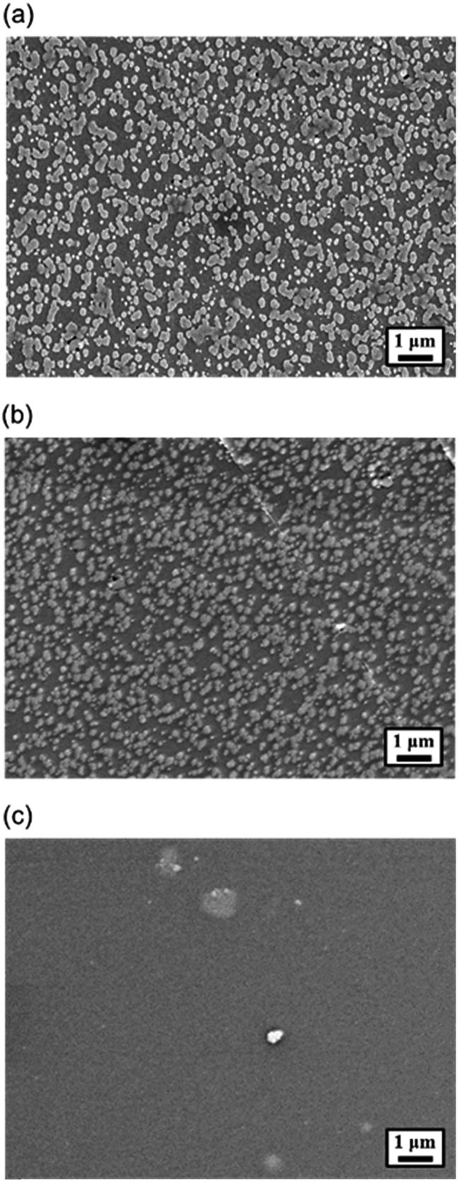 | ||
| Fig. 2 The top-view SEM image of (a) the electrodeposited SnO2, (b) the electrodeposited SnO2/PCBM, and (c) PCBM films on the ITO/PEN flexible substrate. | ||
To address this deficiency, we therefore introduced an additional PCBM layer onto the deposited SnO2 layer. The fullerene materials have not only been demonstrated as efficient ETLs for PVSCs,36,37 but also been proven as sufficient surface modifiers of TMO-based ETLs to facilitate the charge transfer and transport between them and perovskite in the conventional n-i-p PVSCs.38 Shown in Fig. 2b and c are the SEM surface images of the SnO2/PCBM and simplex PCBM layers deposited on the ITO/PEN substrates, respectively. As can be seen, the simplex PCBM clearly exhibited a featureless surface morphology, revealing its superior film formation capability. After adding this layer onto the pre-electrodeposited SnO2 layer, the originally rough surface was kind of flattened and the pristine sharp edges of discrete SnO2 domains was smoothened, indicating that PCBM layer covered the entire surface to avoid any direct contact between perovskite and ITO electrode.
The local surface morphology of these studied ETLs on the ITO/PEN substrate was further characterized using AFM as presented in Fig. 3. As seen, the in-plane continuity of the prepared films is identified, wherein the discrete large grains were observed in the SnO2 film, consistent with its corresponding SEM image (Fig. 2a). Notably, the root-mean-squire (RMS) roughness (Rq) for the SnO2 film and SnO2/PCBM film was evaluated to be 19.4 nm and 12.1 nm, respectively. The significant decrease in Rq affirms the passivation function of the PCBM layer. The smoothened surface of this bilayered ETL is essential for realizing homogeneous deposition of perovskite to result in high performance.
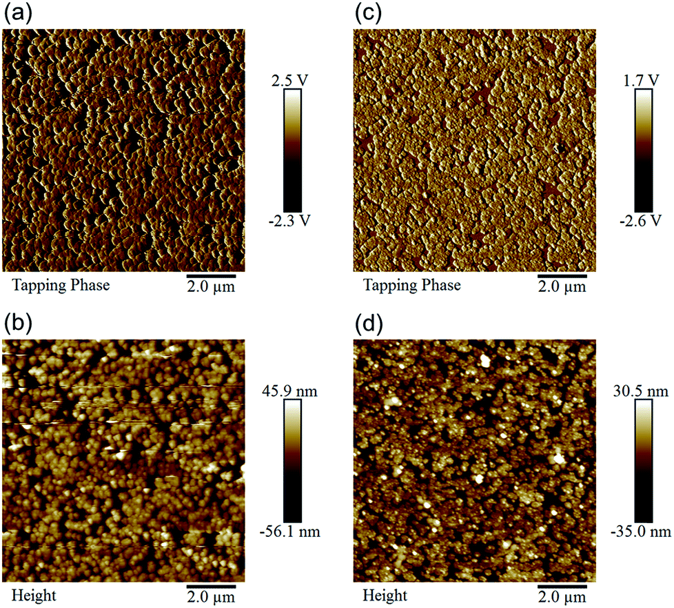 | ||
| Fig. 3 The AFM phase (a and c) and height (b and d) images of the electrodeposited SnO2 film (a and b) and the electrodeposited SnO2/PCBM (c and d) layers on the ITO/PEN flexible substrate. | ||
In addition to the morphological issue, high transparency is another important index for a qualified ETL for achieving high efficiency since it can prevent the parasitical absorption of perovskite absorber. Fig. 4a compared the transmittance spectra of the electrodeposited SnO2 and the electrodeposited SnO2/PCBM films on the ITO/PEN substrates. As can be seen, the bilayered ETL can still possess a reasonable transmittance of ∼80% in the range of wavelengths large than 600 nm despite the slightly decreased transmittance below 600 nm as a result of the absorption of the PCBM layer. Note that the transmittance dramatically decreased at ∼400 nm which is attributed to the absorption of ITO/PEN substrate.
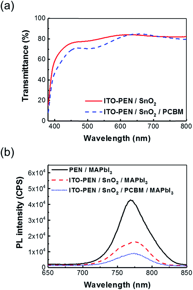 | ||
| Fig. 4 (a) The optical transmittance of the studied ETLs deposited on ITO/PEN substrate and (b) the PL spectra of perovskite and perovskite deposited on the studied ETLs. | ||
In order to evaluate the efficiency of charge transfer between the prepared ETLs and perovskite layer, the photoluminescence (PL) of the ETL/perovskite samples were measured accordingly as portrayed in Fig. 4b. It clearly showed that the PL quenching of CH3NH3PbI3 deposited on a SnO2/PCBM film is higher than the one grown on a simplex SnO2 film, suggesting the facilitated charge transfer between SnO2/PCBM and perovskite. This result is expectable as considering the improvement in morphology as discussed earlier.
To examine the efficacy of the prepared ETLs on a flexible substrates, a convention PVSC consisting of PEN/ITO/studied ETLs/CH3NH3PbI3/Spiro-OMeTAD/Au (Fig. 5, left) was primarily fabricated and the cross-sectional SEM image of the representative device using SnO2/PCBM ETL was present in Fig. 5 (right) to illustrate its well mutli-layered architecture, in which the thickness of SnO2, CH3NH3PbI3, and Spiro-OMeTAD is estimated to be ∼20 nm, 250 nm, and 150 nm, respectively.
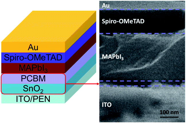 | ||
| Fig. 5 Device structure and the corresponding cross-sectional SEM image. | ||
As a point of note, in order to develop a stable flexible PVSC, we capped the completed device with a ductile elastomer (Scheme 1). As discussed earlier, a thin glass cover slip is the most widely adopted encapsulating technique to date. Its rigidity however impedes the further applications on flexible electronics. Hence, the ductile elastomer was chose as the encapsulating material regarding its easy accessibility, decent adhesion, and good isolation for external substances. Shown in Fig. S2† is the performance comparison of the control devices using a glass slide and an elastomer as the encapsulating layer. Encouragingly, both encapsulating materials can yield similar performance, qualifying the commercial elastomer as a feasible encapsulating material. Provided the good adhesive property of the elastomer, it might not only can serve as a laudable encapsulating material for flexible PVSCs but also can facilitate the fabrication of textile-based PVSCs (Scheme 1), enriching their application values.
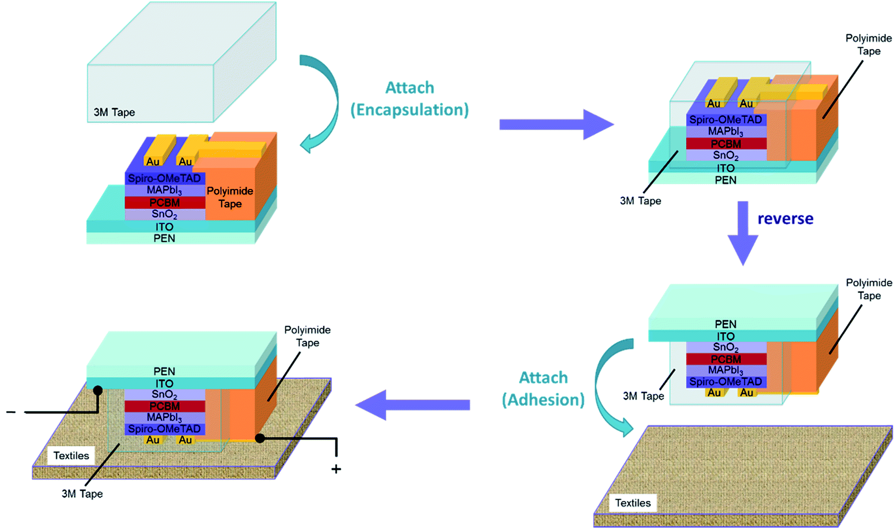 | ||
| Scheme 1 Illustration of the fabrication of the textile-based flexible PVSC via a functional encapsulating layer in this work. | ||
Fig. 6a presented the J–V characteristics of the encapsulated flexible PVSCs using different ETLs measured under 0.8 sun and 1.0 sun illumination and the corresponding photovoltaic parameters are summarized in Table 1. It is deserved to mention that we found out there is no performance difference before and after integrating the encapsulated PVSC on the textile (Scheme 1). This result reflects the merit of using elastomer as the encapsulating materials and demonstrates its convenience of integration onto arbitrary substrates.
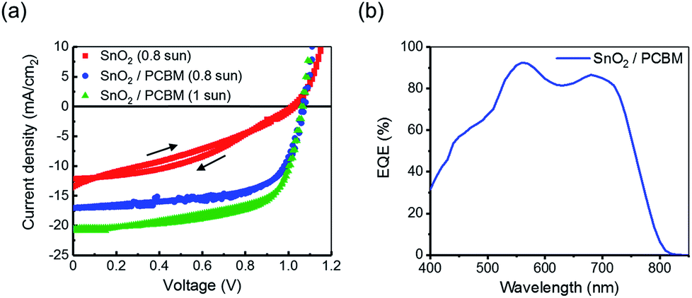 | ||
| Fig. 6 (a) The J–V curves of the studied flexible PVSCs using the electrodeposited SnO2 ETL and SnO2/PCBM ETL. (b) EQE of the PVSC using SnO2/PCBM ETL under 1 sun. | ||
| Electron-transporting layer | VOC (V) | JSC (mA cm−2) | FF | PCE (%) | |
|---|---|---|---|---|---|
| a F: forward-bias sweep (−0.1 V → 1.2 V); R: reverse-bias sweep (1.2 V → −0.1 V).b Time of electrodeposition for SnO2: 120 s. | |||||
| SnO2 (0.8 sun)b | Fa | 1.03 | −13.47 | 0.31 | 5.4 |
| Ra | 1.02 | −12.16 | 0.41 | 6.3 | |
| SnO2/PCBM (0.8 sun) | Fa | 1.08 | −17.07 | 0.63 | 14.5 |
| Ra | 1.06 | −17.05 | 0.65 | 14.8 | |
| SnO2/PCBM (1 sun) | Fa | 1.07 | −20.90 | 0.62 | 13.9 |
| Ra | 1.06 | −20.53 | 0.66 | 14.3 | |
As clearly shown, under 0.8 sun illumination, the control device using simplex electrodeposited SnO2 ETL yielded a low photocurrent along with a poor fill factor (FF), which can be traced to the high series resistance (Rs) and low shunt resistance (Rsh) caused by low-quality SnO2 layer as discussed earlier. Its discontinuous morphology associated with isolated island-like domains impedes efficient charge transport and beget severe charge recombination. However, after introducing a thin PCBM layer, the resultant performance can be significantly improved. As shown, under 0.8 sun illumination, the VOC was improved from 1.02 V to 1.06 V, JSC was raised from 12.16 mA cm−2 to 17.05 mA cm−2, and FF was enhanced from 0.41 to 0.65, corresponding to an increased PCE from 6.3% to 14.8%. This result clearly highlights the pivotal role of PCBM in our fabricated flexible device, which not only smoothens the rough surface of electrodeposited SnO2 film but also facilitates the charge transfer and transport at the corresponding interface. While this top-performing device was measured under 1 sun illumination, the resultant JSC was accordingly increased while the VOC and FF were remained, for which a PCE of 14.3% comparable to the value measured under 0.8 sun illumination is obtained. The external quantum efficiency (EQE) spectrum of this optimized SnO2/PCBM-based device is presented in Fig. 6b. As seen, it showed a broad photo-response across 400 nm to 800 nm, in a good agreement with the light-harvesting behavior of CH3NH3PbI3.39 We note that the lower EQE efficiency across from 400 nm to 520 nm might be ascribed to the parasitic absorption from the hybrid ETL and the substrate and the dip at ∼630 nm might be attributed to the reduced absorption of the perovskite as a result of optical interference.40
Notably, we also fabricated the devices on the regular ITO/glass substrate for a fair comparison and the results were shown in Fig. S3 and Table S1.† As shown, different to the case of using flexible substrate, there is only slight performance difference between the SnO2-based device and SnO2/PCBM-based device. Both devices exhibited hysteresis-free J–V characteristics and yields PCEs of ∼14%. This suggests the high-quality SnO2 can be successfully achieved on the ITO/glass substrate through electrodeposition15 and the additional PCBM interlayer therefore plays a less important role. On the other hand, we have also investigated the feasibility of replacing SnO2 ETL with a PCBM ETL on the flexible ITO/PFN substrate. As shown in Fig. S4 and Table S2,† the device using a simplex PCBM ETL yield a lower JSC than the SnO2-based devices. In addition, it showed severe device hysteresis as reported in the literature.41
We next evaluated the ambient stability of the fabricated textile-based flexible PVSC. In order to understand the encapsulating efficacy of elastomer, flexible PEN-based devices with and without encapsulation were compared in parallel in an ambient condition with a controlled humidity of 65%. As shown in Fig. 7, the encapsulated textile-based device showed a much enhanced ambient stability, for which over 70% of initial PCE can be maintained after 425 h storage. In contrast, the unencapsulated device was quickly degraded within 100 h due to the poor surface barrier properties of Spiro-OMeTAD42 and the fragility of perovskite to oxygen and moisture.43,44 As mentioned above, our device shows good performance at first days of operation but possesses poor stability without encapsulation, indicating that Spiro-OMeTAD is not suitable for serving as an effective surface barrier for H2O and O2 diffusion. Further optimization using more advanced HTLs is in progress in our group.
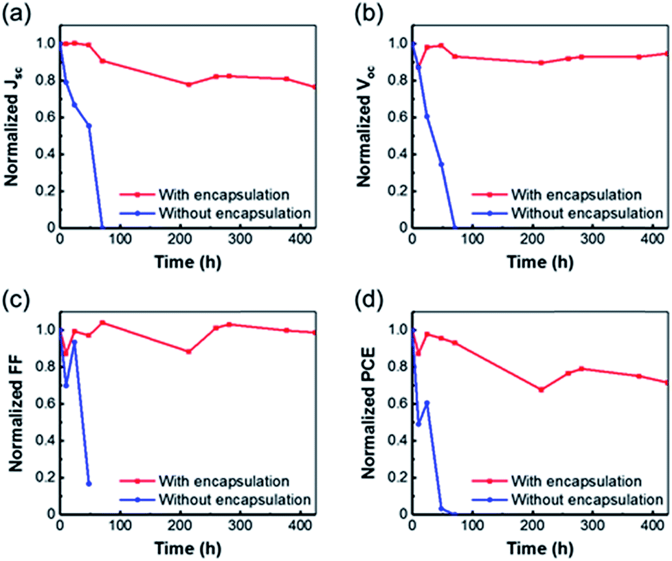 | ||
| Fig. 7 Device performance of the textile-based flexible PVSC (red square) and the reference PVSC without encapsulation (blue dot) as a function of storage time in an ambient environment (humidity: ∼65%; T = 25 °C). (a) Normalized JSC, (b) normalized VOC, (c) normalized FF, and (d) normalized PCE. | ||
Besides the ambient stability, we also examined the water-resistance of the textile-based PVSC in an extreme case, for which the whole device stack was immersed into water for a certain period of time as shown in Fig. 8a. Presented in Fig. 8b is a photograph comparing the devices with and without encapsulation. As can be clearly seen, the color of the unencapsulated part was immediately (<1 s) turned into yellow and completely lost the photovoltaic performance. Whereas, the encapsulated device can still preserve a comparable performance after 35 minute immersion in water as displayed in Fig. 8c, for which only a slight decrease in Jsc was observed. These encouraging results manifested that the elastomer can effectively isolate the penetration of air and water into device, enhancing the washable abilities of the encapsulated flexible PVSC, which is very critical for the future potential applications in the wearable devices.
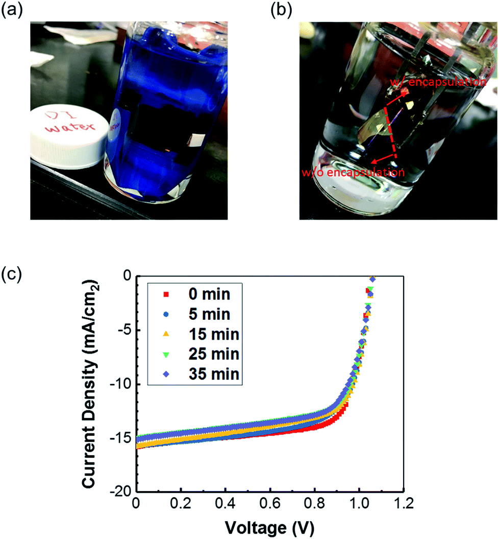 | ||
| Fig. 8 Photos of (a) the textile-based flexible PVSC immersing in water and (b) a designed device with and without encapsulation immersing in water. (c) The J–V curve of the textile-based flexible PVSC as a function of immersing time in water. | ||
With the successful realization of an efficient textile-based flexible PVSC (Fig. 9a), we further utilized this proof-of-concept device to demonstrate some possible applications in wearable electronics. For example, we arranged the integrated PVSCs on textile in series connection to successfully light up a commercial light-emitting diode integrated on the same textile as displayed in Fig. 9b. This result suggests our novel device design not only can deliver a stable and efficient flexible PVSC but also can enrich the device's functionality in wearable devices to serve as an efficient power supply system.
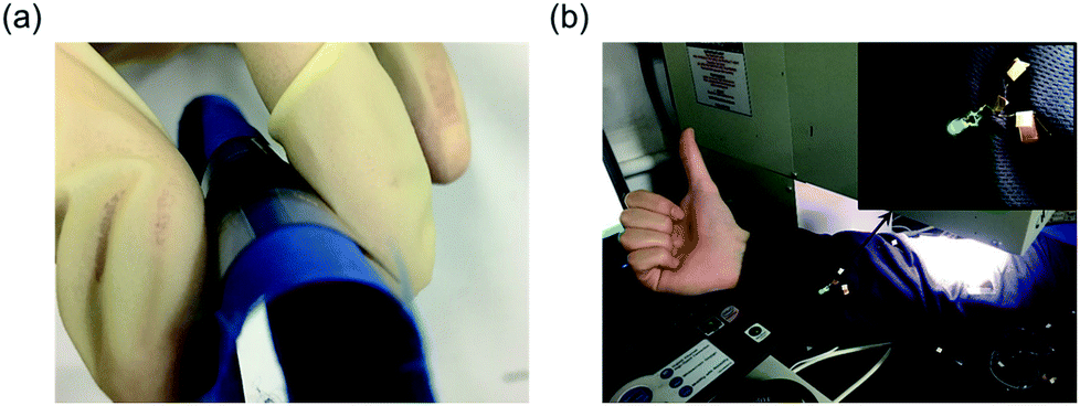 | ||
| Fig. 9 Photos of (a) the textile-based flexible PVSC and (b) a commercial LED lit up by the fabricated textile-based flexible PVSCs under 0.8 sun illumination. | ||
Conclusion
In this work, we successfully developed an efficient textile-based flexible PVSC by employing a low-temperature electrodeposited SnO2 ETL coupled with a thin PCBM ETL and a functional encapsulating layer. Different to our previous work,15 we unexpectedly revealed that the quality of the low-temperature electrodeposited SnO2 film on flexible ITO/PEN substrate is inferior to the film deposited on regular rigid substrate, attributed to the lower conductivity of ITO on the flexible substrate. Fortunately, introducing an additional PCBM layer can compensate this deficiency. Besides, we demonstrated that an easily accessible elastomer can effectively encapsulate the fabricated flexible PVSC, as exemplified by the largely improved ambient stability and waterproof property. Moreover, benefiting from its good adhesive property, the completed device stack can be effortlessly integrated onto a textile substrate, showing a much improved deployable capability. As a result, a ∼15% textile-based flexible PVSC with improved ambient stability and washable capability was demonstrated. A proof-of-concept device was successfully integrated with other electronic devices on the textile to serve as an efficient power supply system, demonstrating its promising potential for the wearable device applications.Experimental
Preparation of SnO2 via electrodeposition method
All materials and chemicals were used as received unless stated otherwise. The electrodeposition of SnO2 films on indium tin oxide (ITO)-coated glass substrates follows our previously reported method.15 The ITO/PEN substrates were cleaned with detergent and then sequentially ultra-sonicated in deionized water, acetone, and isopropanol for 15 min, respectively. Afterward, the substrates were dried at 120 °C for 10 min, followed by UV-ozone exposure for 20 min. The electrochemical deposition was performed on a CHI 611D electrochemical analyzer using a three-electrode cell in which ITO was used as a working electrode. A platinum wire was used as a counter-electrode and an Ag/AgCl electrode (with a potential at +0.22 V vs. standard hydrogen electrode) was used as the reference electrode. The deposition solution is made of 20 mM SnCl2, 100 mM NaNO3 and 75 mM HNO3 dissolved in de-ionized water. For the deposition of SnO2 thin film, ITO/PEN without using a seed layer was placed in deposition bath and a constant voltage of −0.4 V vs. Ag/AgCl reference electrode was applied for 120 s under 50 °C.Fabrication of planar perovskite solar cells
All fabrication processes except for the SnO2 electrodeposition were operated in an N2-filled glove box. A thin PCBM (∼10 mg ml−1 in chlorobenzene) layer was spin-coated onto the SnO2 coated-ITO/PEN substrate at 1000 rpm for 60 s. A 1 M precursor solution of perovskite was prepared by dissolving lead iodide (PbI2, 1 mmol) and methylammonium iodide (CH3NH3I, 1 mmol) in a 7![[thin space (1/6-em)]](https://www.rsc.org/images/entities/char_2009.gif) :3 v/v γ-butyrolactone/dimethyl sulfoxide binary solvent mixture. The perovskite layer was prepared through the solvent washing technique by consecutive three steps: 500 rpm for 5 s, 1000 rpm for 45 s, and 5000 rpm for 40 s. During the spin-coating, anhydrous toluene was in situ dropped at 20 s prior to the stop to facilitate the conversion of intermediate iodoplumbate anions to perovskite.45,46 The deposited perovskite film was subsequently annealed at 100 °C for 10 min. The hole-transporting layer (HTL) was deposited by spin coating a 40 mg ml−1 concentration of 2,2′,7,7′-tetrakis(N,N-di-p-methoxyphenylamine)-9,9′-spirobifluorene (spiro-OMeTAD) solution in chlorobenzene added with 33 μl of lithium bis(trifluoromethanesulfonyl) imide (Li-TFSI) solution (175.1 mg Li-TSFI in 1 ml acetonitrile, Sigma-Aldrich, 99.8%) and 16 μl of 4-tert-butyl pyridine (tBP) at the speed of 2000 rpm for 60 s. After depositing the HTL, the samples were stored inside a desiccator for a designated period of time. Finally, Au electrodes were thermally evaporated under high vacuum through a shadow mask to complete the device fabrication.
:3 v/v γ-butyrolactone/dimethyl sulfoxide binary solvent mixture. The perovskite layer was prepared through the solvent washing technique by consecutive three steps: 500 rpm for 5 s, 1000 rpm for 45 s, and 5000 rpm for 40 s. During the spin-coating, anhydrous toluene was in situ dropped at 20 s prior to the stop to facilitate the conversion of intermediate iodoplumbate anions to perovskite.45,46 The deposited perovskite film was subsequently annealed at 100 °C for 10 min. The hole-transporting layer (HTL) was deposited by spin coating a 40 mg ml−1 concentration of 2,2′,7,7′-tetrakis(N,N-di-p-methoxyphenylamine)-9,9′-spirobifluorene (spiro-OMeTAD) solution in chlorobenzene added with 33 μl of lithium bis(trifluoromethanesulfonyl) imide (Li-TFSI) solution (175.1 mg Li-TSFI in 1 ml acetonitrile, Sigma-Aldrich, 99.8%) and 16 μl of 4-tert-butyl pyridine (tBP) at the speed of 2000 rpm for 60 s. After depositing the HTL, the samples were stored inside a desiccator for a designated period of time. Finally, Au electrodes were thermally evaporated under high vacuum through a shadow mask to complete the device fabrication.
Integration of fabricated device on textiles
The integration of the fabricated flexible PVSCs on textiles was illustrated in Scheme 1. The 3M™ acrylic elastomer (3M™ VHB™ 4905) was used as received and the textiles were provided by Taiwan textile research institute (TTRI). The 3M™ elastomer was first attached on device's top side which deployed metal electrodes and then the whole device stack were reversed to adhere to the textile.Characterization
Transmission electron microscope (TEM) images and selected-area electron diffraction (SAED) pattern were taken using a microscope (FEI Tecnai G2 20) operated at 200 keV to observe the crystallographic orientation of the electrodeposited SnO2 film. Scanning electron microscopy (SEM) imaging was taken using field emission scanning electron microscope (FE-SEM, JEOL JSM-6700F, Japan). Atomic force microscopy (AFM) imaging was performed on Innova (Bruker, Germany) AFM system in a tapping mode in air. The UV-vis transmission spectrum was recorded using a Hitachi U-4100 spectrophotometer. Photoluminescence (PL) spectra were measured by Horiba Fluorolog-3. For the current density–voltage (J–V) measurement, the devices (with an active area of 0.04 cm2) were characterized under illumination of a Newport solar simulator (Newport Corp., Irvine, CA USA) with ∼800 W m−2 (∼0.8 sun) intensity calibrated with a silicon reference diode. The J–V characteristics were recorded using a source meter (Keithley 2400, USA) in reverse (from the open-circuit voltage (VOC) to the short-circuit current (JSC)) and forward (from JSC to VOC) scan directions at a sweeping rate of 0.1 V s−1. Reference ITO/glass-based device was characterized using the same conditions.Stability of the integrated device (with encapsulation) on textiles and reference device without encapsulation was monitored up to 425 h. The studied devices were stored in an ambient environment at 25 °C with a relative humidity of 65%. Water resistance test was carried out by immersing the integrated device into water without any further treatment. The tested device was took out at a certain period of time for performance checking and the residual water was gently wiped out by tissue prior to the J–V measurement.
Conflicts of interest
There are no conflicts to declare.Acknowledgements
The authors acknowledge the financial support from the Ministry of Science and Technology of Taiwan (MOST 105-2119-M-002-008 & 106-2218-E-002-021-MY2) and Top University Project from National Taiwan University (106R7322).Notes and references
- Q. Chen, H. Zhou, Z. Hong, S. Luo, H.-S. Duan, H.-H. Wang, Y. Liu, G. Li and Y. Yang, J. Am. Chem. Soc., 2014, 136, 622–625 CrossRef CAS PubMed.
- G. Niu, X. Guo and L. Wang, J. Mater. Chem. A, 2015, 3, 8970 CAS.
- M. B. Johnston and L. M. Herz, Acc. Chem. Res., 2016, 49, 146 CrossRef CAS PubMed.
- G. Xing, N. Mathews, S. Sun, S. S. Lim, Y. M. Lam, M. Grätzel, S. Mhaisalkar and T. C. Sum, Science, 2013, 342, 344 CrossRef CAS PubMed.
- W. S. Yang, J. H. Noh, N. J. Jeon, Y. C. Kim, S. Ryu, J. Seo and S. I. Seok, Science, 2015, 348, 1234 CrossRef CAS PubMed.
- N. J. Jeon, J. H. Noh, Y. C. Kim, W. S. Yang, S. Ryu and S. I. Seok, Solvent engineering for high-performance inorganic-organic hybrid perovskite solar cells, Nat. Mater., 2014, 13, 897 CrossRef CAS PubMed.
- S. T. Williams, A. Rajagopal, C.-C. Chueh and A. K. Y. Jen, J. Phys. Chem. Lett., 2016, 7, 811 CrossRef CAS PubMed.
- National Renewable Energy Laboratory (NREL), Research cell record efficiency chart, https://www.nrel.gov/pv/assets/images/efficiency-chart.png, July 2017.
- D. Bi, W. Tress, M. I. Dar, P. Gao, J. Luo, C. Renevier, K. Schenk, A. Abate, F. Giordano, J.-P. Correa Baena, J.-D. Decoppet, S. M. Zakeeruddin, M. K. Nazeeruddin, M. Grätzel and A. Hagfeldt, Sci. Adv., 2016, 2, e1501170 Search PubMed.
- H. Zhang, H. Azimi, Y. Hou, T. Ameri, T. Przybilla, E. Spiecker, M. Kraft, U. Scherf and C. J. Brabec, Chem. Mater., 2014, 26, 5190 CrossRef CAS.
- F. Giordano, A. Abate, J. P. C. Baena, M. Saliba, T. Matsui, S. H. Im, S. M. Zakeeruddin, M. K. Nazeeruddin, A. Hagfeldt and M. Graetzel, Nat. Commun., 2016, 7, 10379 CrossRef CAS PubMed.
- M.-C. Wu, S.-H. Chan, M.-H. Jao and W.-F. Su, Sol. Energy Mater. Sol. Cells, 2016, 157, 447 CrossRef CAS.
- H.-S. Kim and N.-G. Park, J. Phys. Chem. Lett., 2014, 5, 2927 CrossRef CAS PubMed.
- G. E. Eperon, V. M. Burlakov, P. Docampo, A. Goriely and H. J. Snaith, Adv. Funct. Mater., 2014, 24, 151 CrossRef CAS.
- J.-Y. Chen, C.-C. Chueh, Z. Zhu, W.-C. Chen and A. K.-Y. Jen, Sol. Energy Mater. Sol. Cells, 2017, 164, 47 CrossRef CAS.
- B. J. Kim, D. H. Kim, Y.-Y. Lee, H.-W. Shin, G. S. Han, J. S. Hong, K. Mahmood, T. K. Ahn, Y.-C. Joo, K. S. Hong, N.-G. Park, S. Lee and H. S. Jung, Energy Environ. Sci., 2015, 8, 916 CAS.
- D. Liu, M. K. Gangishetty and T. L. Kelly, J. Mater. Chem. A, 2014, 2, 19873 CAS.
- H. Tan, A. Jain, O. Voznyy, X. Lan, F. P. García de Arquer, J. Z. Fan, R. Quintero-Bermudez, M. Yuan, B. Zhang, Y. Zhao, F. Fan, P. Li, L. N. Quan, Y. Zhao, Z.-H. Lu, Z. Yang, S. Hoogland and E. H. Sargent, Science, 2017, 355, 722 CrossRef CAS PubMed.
- S. S. Shin, E. J. Yeom, W. S. Yang, S. Hur, M. G. Kim, J. Im, J. Seo, J. H. Noh and S. I. Seok, Science, 2017, 14, 167 CrossRef PubMed.
- E. H. Anaraki, A. Kermanpur, L. Steier, K. Domanski, T. Matsui, W. Tress, M. Saliba, A. Abate, M. Grätzel, A. Hagfeldt and J.-P. Correa-Baena, Energy Environ. Sci., 2016, 9, 3128 CAS.
- W. Ke, G. Fang, Q. Liu, L. Xiong, P. Qin, H. Tao, J. Wang, H. Lei, B. Li, J. Wan, G. Yang and Y. Yan, J. Am. Chem. Soc., 2015, 137, 6730 CrossRef CAS PubMed.
- M. Kaltenbrunner, G. Adam, E. D. Głowacki, M. Drack, R. Schwödiauer, L. Leonat, D. H. Apaydin, H. Groiss, M. C. Scharber, M. S. White, N. S. Sariciftci and S. Bauer, Nat. Mater., 2015, 14, 1032 CrossRef CAS PubMed.
- J. A. Christians, P. A. M. Herrera and P. V. Kamat, J. Am. Chem. Soc., 2015, 137, 1530 CrossRef CAS PubMed.
- J. M. Frost, K. T. Butler, F. Brivio, C. H. Hendon, M. van Schilfgaarde and A. Walsh, Nano Lett., 2014, 14, 2584 CrossRef CAS PubMed.
- J. Yang, B. D. Siempelkamp, D. Liu and T. L. Kelly, ACS Nano, 2015, 9, 1955 CrossRef CAS PubMed.
- H. Kim, K.-G. Lim and T.-W. Lee, Energy Environ. Sci., 2016, 9, 12 CAS.
- T. A. Berhe, W.-N. Su, C.-H. Chen, C.-J. Pan, J.-H. Cheng, H.-M. Chen, M.-C. Tsai, L.-Y. Chen, A. A. Dubale and B.-J. Hwang, Energy Environ. Sci., 2016, 9, 323 CAS.
- Y. Han, S. Meyer, Y. Dkhissi, K. Weber, J. M. Pringle, U. Bach, L. Spiccia and Y.-B. Cheng, J. Mater. Chem. A, 2015, 3, 8139 CAS.
- D. Yu, Y.-Q. Yang, Z. Chen, Y. Tao and Y.-F. Liu, Opt. Commun., 2016, 362, 43 CrossRef CAS.
- J.-S. Park, H. Chae, H. K. Chung and S. I. Lee, Semicond. Sci. Technol., 2011, 26, 034001 CrossRef.
- M. Jørgensen, K. Norrman and F. C. Krebs, Sol. Energy Mater. Sol. Cells, 2008, 92, 686 CrossRef.
- J. A. Hauch, P. Schilinsky, S. A. Choulis, S. Rajoelson and C. J. Brabec, Appl. Phys. Lett., 2008, 93, 103306 CrossRef.
- W. J. Potscavage, S. Yoo, B. Domercq and B. Kippelen, Appl. Phys. Lett., 2007, 90, 253511 CrossRef.
- C.-Y. Chang, C.-T. Chou, Y.-J. Lee, M.-J. Chen and F.-Y. Tsai, Org. Electron., 2009, 10, 1300 CrossRef CAS.
- K. Shin, J. Park and C. Lee, Thin Solid Films, 2016, 598, 95 CrossRef CAS.
- P.-W. Liang, C.-C. Chueh, S. T. Williams and A. K.-Y. Jen, Adv. Energy Mater., 2015, 5, 1402321 CrossRef.
- J. You, Z. Hong, Y. M. Yang, Q. Chen, M. Cai, T.-B. Song, C.-C. Chen, S. Lu, Y. Liu, H. Zhou and Y. Yang, ACS Nano, 2014, 8, 1674 CrossRef CAS PubMed.
- F. Fu, T. Feurer, T. Jäger, E. Avancini, B. Bissig, S. Yoon, S. Buecheler and A. N. Tiwari, Nat. Commun., 2015, 6, 8932 CrossRef CAS PubMed.
- H.-W. Chen, T.-Y. Huang, T.-H. Chang, Y. Sanehira, C.-W. Kung, C.-W. Chu, M. Ikegami, T. Miyasaka and K.-C. Ho, Sci. Rep., 2016, 6, 34319 CrossRef CAS PubMed.
- O. Malinkiewicz, A. Yella, Y. H. Lee, G. M. Espallargas, M. Graetzel, M. K. Nazeeruddin and H. J. Bolink, Nat. Photonics, 2014, 8, 128 CrossRef CAS.
- H.-S. Kim, I.-H. Jang, N. Ahn, M. Choi, A. Guerrero, J. Bisquert and N.-G. Park, J. Phys. Chem. Lett., 2015, 6, 4633 CrossRef CAS PubMed.
- B. A. Nejand, V. Ahmadi, S. Gharibzadeh and H. R. Shahverdi, ChemSusChem, 2016, 9, 302 CrossRef CAS PubMed.
- D. Bryant, N. Aristidou, S. Pont, I. Sanchez-Molina, T. Chotchunangatchaval, S. Wheeler, J. R. Durrant and S. A. Haque, Energy Environ. Sci., 2016, 9, 1655 CAS.
- Y. Zhao, J. Wei, H. Li, Y. Yan, W. Zhou, D. Yu and Q. Zhao, Nat. Commun., 2016, 7, 10228 CrossRef CAS PubMed.
- D. Bae, A. Palmstrom, K. Roelofs, B. Mei, I. Chorkendorff, S. F. Bent and P. C. K. Vesborg, ACS Appl. Mater. Interfaces, 2016, 8, 14301 CAS.
- N. Ahn, D.-Y. Son, I.-H. Jang, S. M. Kang, M. Choi and N.-G. Park, J. Am. Chem. Soc., 2015, 137, 8696 CrossRef CAS PubMed.
Footnote |
| † Electronic supplementary information (ESI) available. See DOI: 10.1039/c7ra10321b |
| This journal is © The Royal Society of Chemistry 2017 |