
 Open Access Article
 This Open Access Article is licensed under a
 Creative Commons Attribution 3.0 Unported Licence
Enhanced performance of perovskite solar cells by strengthening a self-embedded solvent annealing effect in perovskite precursor films†
Xiaobing Caoa,
Lili Zhib,
Yahui Lia,
Xian Cuia,
Lijie Ci b,
Kongxian Dingc and
Jinquan Wei*a
b,
Kongxian Dingc and
Jinquan Wei*a
aState Key Lab of New Ceramic and Fine Processing, School of Materials Science and Engineering, Tsinghua University, Beijing 100084, P. R. China. E-mail: jqwei@tsinghua.edu.cn
bSchool of Materials Science and Engineering, Shandong University, Jinan 250061, Shandong, P. R. China
cShenzhen Jiawei Solar Lighting Co., Ltd., Fuping Road, New Industrial Zone No. 1-4, Longgang District, Shenzhen 518112, Guangdong, P. R. China
First published on 20th October 2017
Abstract
The solvent embedded in the intermediate phase is widely observed in the fabrication of perovskite films. The perovskite precursor films obtained from Lewis adducts through molecular exchange contain some residue solvent. It has an intrinsic solvent annealing effect during the annealing process. Here, we pre-deposit a protective layer on the perovskite precursor films to retard the escape of solvent during the annealing process. The restricted solvent strengthens the solvent annealing effect during the formation of perovskite films. As a result, the perovskite quality, including grain size and crystallization, is improved significantly, which leads to efficient charge transportation, low recombination rate, and enhancement of the photovoltaic performance of the corresponding perovskite solar cells.
1. Introduction
The efficiency of perovskite solar cells (PSCs) has been boosted from an initial 3.8% to 22.1% in recent years.1,2 The most important approach to obtain highly efficient PSCs is to improve the quality of the light harvest layer in PSCs, including improving morphology,3,4 increasing perovskite grain size,5,6 improving crystallization7,8 and optimizing composition.9 Among all these approaches, we need basically to improve the photovoltaic performance by increasing the perovskite grain size. The large perovskite grains can reduce trap density, which is beneficial to improve the performance10 and stability11 of the perovskite solar cells.Up to now, various methods have been proposed to fabricate smooth perovskite films with large grains. For example, Nie et al. reported a solution-based hot-cast technique to grow high quality perovskite film with millimeter-scale crystalline grains.12 Xiao et al. adopted a fast deposition–crystallization processing for obtaining uniform perovskite films with large grains.13 Yang et al. developed a facile method to obtain large grain of CH3NH3I3−xBrx via an Ostwald ripening process by a simple MABr solution treatment.14 Different additives were added into precursor solutions to increase perovskite grains.15,16 Especially, Huang's group reported a novel solvent annealing to obtain large perovskite grains with excellent crystallinity.17 Typically, the solvent annealing process is as following: the perovskite film is exposed to different solvent (e.g., DMF, DMSO) in a Petri dish by optimizing annealing time and temperature.18,19 This process can promote the formation of large perovskite grains with excellent crystallization. However, the experiment condition for solvent annealing, such as the amount and distribution of solvent, annealing time, annealing temperature are extremely strict. The strict experiment conditions make it is difficult to fabricate high quality perovskite films with good reproducibility.20
The perovskite films fabricated through solution-based processing are usually intermediate phases contained some organic solvent molecules, and then the intermediate phases transform to perovskite film by removing solvent through annealing treatment. It has been a widely accepted fact that solvent embedded in intermediate phase play a key role in retarding the rapid reaction between PbI2 and MAI during the formation of high quality perovskite films.21–23 In our previous work, we fabricated smooth perovskite films from Lewis adducts through molecular exchange through a modified two-step method.24 The smooth perovskite films were ascribed to the solvent modulated the formation of perovskite film during molecular exchange and annealing process.25 It is solvent included perovskite precursor film, which is the product obtained after molecule exchange between solvent and MAI. We believe that the solvent molecule embedded in the perovskite precursor film may induce weak solvent annealing during annealing.
Here, we make use of the solvent embedded in the perovskite precursor films to induce an obvious solvent annealing effect. In order to retard the escape of the solvent, we pre-deposit a protective layer onto the perovskite precursor film before annealing. The restrained solvent strengthens the solvent annealing effect during annealing process, resulting in formation of smooth perovskite film with large grains.
2. Experimental
Fabrication of the devices
The clean of FTO substrates, deposition of TiO2 blocking layers, and TiO2 mesoporous layers have been described in details in our previous report.24 Perovskite films were fabricated through a modified two-step method.24 A layer of PbI2 precursor film was firstly spin-coated from PbI2/DMF (1.4 M) solution at 5500 rpm for 30 s, and then dipped into a solution of CH3NH3I (MAI)/2-propanol with concentration 30 mg mL−1 for 60 s to prepare perovskite precursor film. Here, we employ two different annealing approach on perovskite precursor film: traditional annealing approach without protective layer and sealed-style annealing approach with a protective layer onto perovskite precursor film. In traditional annealing approach, the perovskite precursor film was directly annealed at 100 °C for 120 min to obtain perovskite film. In the sealed-style annealing approach, a PC61BM protective layer was deposited on the top of perovskite precursor film, and then annealed at 100 °C for 120 min to obtain perovskite film. The PC61BM protective layer was washed by chlorobenzene several times before depositing a hole transportation layer. The hole transportation layer was deposited by spin-coating from HTL solution (100 mg Spiro-OMeTAD, 40 μL 4-tert-butylpyridine (tBP), 36.3 μL (520 mg mL−1 TFSI in acetonitrile) and 60 μL FK102 (300 mg mL−1 in acetonitrile) in 1 mL chlorobenzene). Finally, a gold electrode was deposited on HTL to form a complete perovskite solar cell. The active area of the electrode was fixed at 0.06 cm2.Characterization
The perovskite films were characterized by field-emission scanning electron microscopy (SEM, MERLIN VP Compact), atomic force microscopy (AFM5500, Agilent), X-ray diffraction (XRD, D8-Advance), and UV/Vis absorption spectrometer (Cary 5000 UV-vis-NIR, Agilent Technologies) in a range from 400 to 900 nm. Impedance spectra were measured by using an electrochemical workstation (CHI660D) in dark under a bias voltage of 0.9 V and an alternative signal of 10 mV in frequency range from 1 Hz to 106 Hz. Steady photoluminescence (PL) spectra were measured by an Edinburgh FLS 920 instrument (Livingston, UK) excited by monochromatic xenon lamp source (central wavelength λ = 460 nm). Time-resolved PL spectra were measured by a time-correlated single photon counting (TCSPC) system. The samples were excited by a 405 nm laser beam (EPL-405). The photovoltaic performance of PSCs were measured by using a solar simulator (AM 1.5G, 100 mW cm−2, 91195, Newport). The obtained J–V curves was recorded by Keithley 4200-SCS parameter analyzer sweeping from −0.1 to 1.2 V at a scan rate of 5 mV s−1.3. Results and discussion
Fig. 1 shows an illustration of the fabrication of perovskite by different annealing approaches. It forms Lewis adducts of PbI2·xDMF when the PbI2/DMF solutions was spin-coated onto FTO substrates coated with TiO2 layer. It forms perovskite precursor of MAI–PbI2–DMF when the Lewis adducts were dipped into MAI/IPA solution via molecular exchange. Fig. 1b shows the evolution of XRD curves during the formation of perovskite film. There are two obvious characteristic peaks located at 9.03°, 9.56° at low angle in XRD curves of PbI2·xDMF (red line in Fig. 1b), corresponding to the plane (011) and (020) of the PbI2·xDMF.26 When PbI2·xDMF film is dipped into MAI/IPA solution, it forms perovskite precursor film of MAI–PbI2–DMF, which is characterized by three characteristic peaks located between 5°and 10° in the XRD curve (see blue line in Fig. 1b).27,28 The MAI–PbI2–DMF film then transfer to MAPbI3 by removing the solvent through different annealing approaches. In the traditional annealing approach without protective layer, the perovskite intermediate films are directly annealed at 100 °C for 120 min (see Fig. 1c); while in the sealed-style annealing approach, perovskite intermediate films are covered with a protective layer, and then annealed at 100 °C for 120 min. In previous work, it has been reported that PC61BM may penetrate into grain boundary for suppression of hysteresis of device.29 So we choose PC61BM as protective layer to study the novel annealing approach on the quality of perovskite film. The PC61BM is removed by washing in chlorobenzene solvent for several times (see Fig. 1d).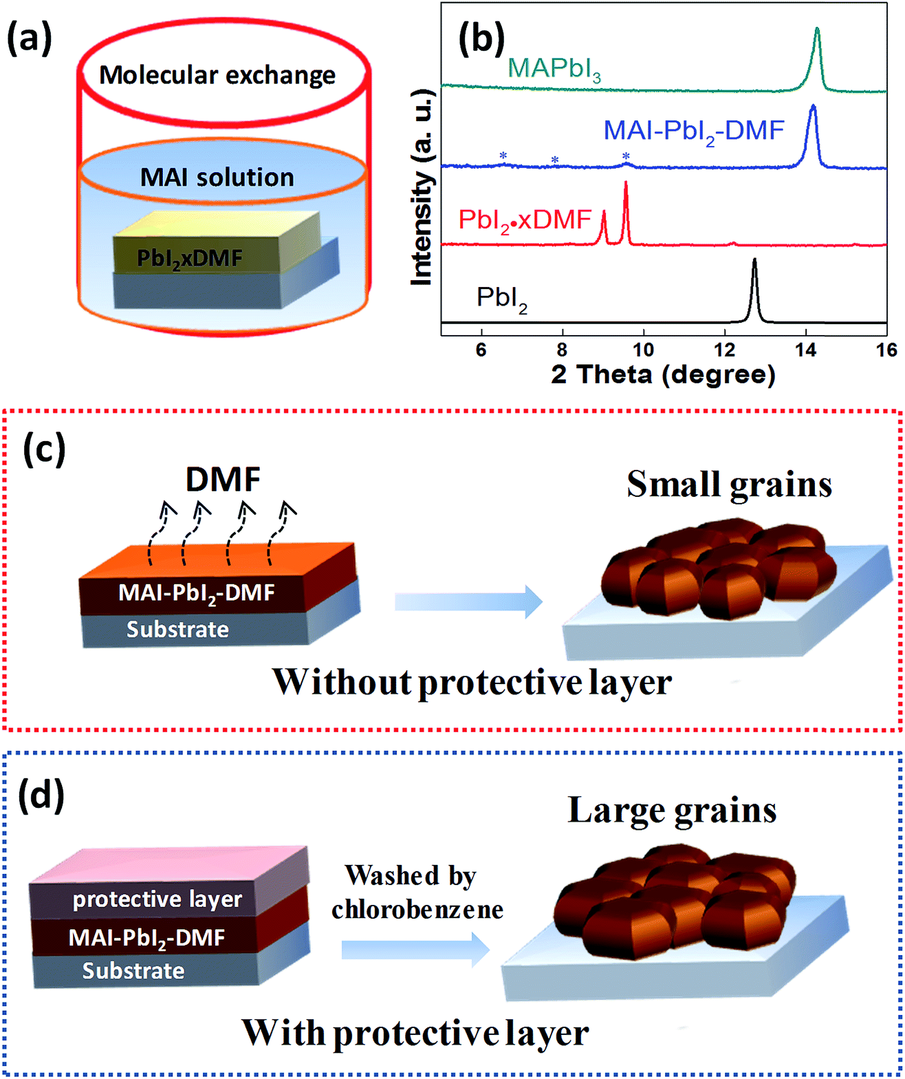 | ||
| Fig. 1 Schematic illustration of the fabrication of perovskite films. (a) Molecular exchange process, (b) evolution of XRD patterns for different films during the formation of perovskite. Different approaches to fabricate perovskite films: (c) without protective layer, (d) with protective layer. | ||
Fig. 2 is SEM images of the perovskite films annealed with and without protective layer. It is clear that the grains size strongly depends on the annealing approach. The average grains size increases from 206 nm to 351 nm (see Fig. S1†), and the average roughness of perovskite film also decrease from 20.3 nm to 13.3 nm (see Fig. S2†), when the perovskite precursor films are covered with a protective layer. Fig. 2b and d are cross-sectional SEM images of the perovskite film fabricated from different annealing approaches. The perovskite capping layers exhibit smooth and hole-free morphology with thickness of ∼340 nm. The perovskite films contain few grain boundaries in the thickness direction fabricated by annealing without PC61BM protective layer, which is ascribed to the small grain size than the perovskite film thickness. However, the perovskite films fabricated by annealing with a protective layer exhibit column-like structure. It contains only one grain in most area, which ascribes to the larger grains size than the film thickness. The column-like structure of perovskite film are extremely desired for high efficient PSCs due to reducing non-radiative charge carrier recombination at grain boundaries.30
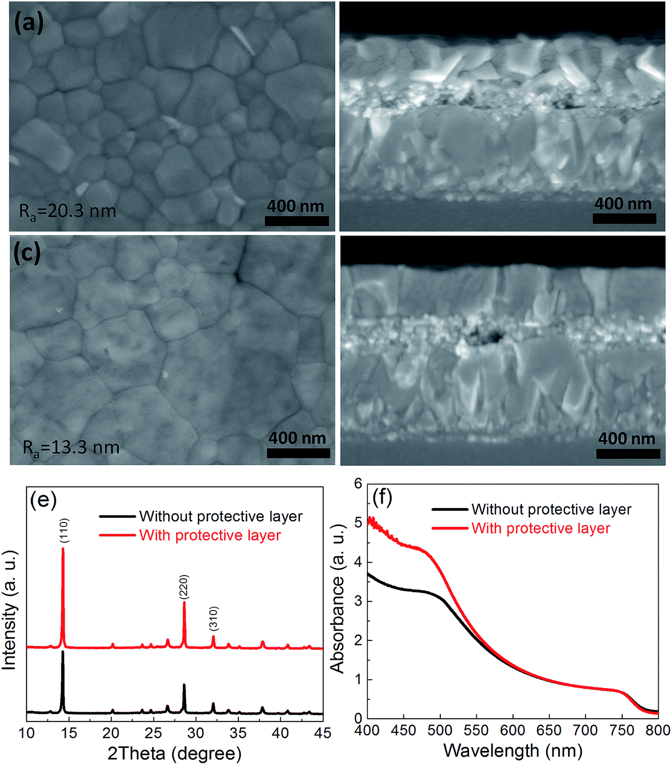 | ||
| Fig. 2 Surface and cross-sectional SEM images of the perovskite films fabricated from different annealing approaches. (a) and (b) are without protective layer, (c) and (d) are with protective layer. (e) XRD patterns and (f) UV-Vis absorption spectra of the perovskite films fabricated from different annealing approaches. | ||
Fig. 2e shows XRD curves of the perovskite films annealed with and without a PC61BM protective layer. All of the XRD curves exhibit several peaks located at 14.3°, 28.6°, and 32.0°, which correspond to the (110), (220) and (310) planes of the MAPbI3, respectively.18 It is noted that the perovskite film annealed with a protective layer exhibits higher crystallization. We introduce intensity ratios of I110/I310 and I220/I310 to evaluate the grain orientation, which denoted as the intensity of (110) and (220) peaks divided by the intensity of (310) peak, respectively.31 The value of I110/I310 and I220/I310 of the perovskite film annealed with a protective layer are 7.53 are 3.54, respectively. For comparison, the corresponding value are only 5.38 and 2.58 for the perovskite annealed without a protective layer. The increase of I110/I310 and I220/I310 indicate that the perovskite grains have a preferred orientation of (110), which is beneficial for the transportation of the carries.31 Fig. 2f shows UV absorption spectra of the perovskite films. The films show an onset at 775 nm, corresponding to the bandgap of MAPbI3 (∼1.55 eV).32 The perovskite film annealed with protective layer exhibits stronger light absorption ability, especially in range from 400 to 550 nm.
The improved crystallization and large grains size of MAPbI3 film can be ascribed to solvent annealing effect caused by DMF molecule embedded in perovskite precursor films. Without protective layer, DMF escape and evaporate from the MAI–PbI2–DMF film easily during annealing process due to its low boiling point (152 °C)33 and weak interaction between Pb2+ and DMF molecule.6,24 The protective layer on the MAI–PbI2–DMF film prevent the DMF from escaping quickly. The restricted DMF induce solvent annealing effects during annealing process. Therefore, the solvent annealing effect response for the improved crystallization and large grains of MAPbI3 films annealed with protective layer.17 We also introduce optimized DMSO into PbI2/DMF solution6 by employing PC61BM as protective layer during annealing. The perovskite grains increase significantly, but it leads to many holes in perovskite film (see Fig. S3†), which have detrimental effects on the photovoltaic performance of PSCs. In order to confirm the university of the new annealing approach, we also use Spiro-OMeTAD (without any additives) as protective layer to retard the escape of DMF molecule, it can also increase perovskite grain size and photovoltaic performance of corresponding devices due to solvent annealing effect (see Fig. S4†).
Fig. 3a is a cross-sectional SEM image of a complete PSCs, showing a geometric structure of the device containing fluorine-doped tin oxide (FTO)/compact-TiO2/mesoporous-TiO2/MAPbI3/Spiro-OMeTAD/Au. As shown in Fig. 3b, we achieved the best photovoltaic performance of the PSCs fabricated from different annealing approaches by employing this structure. The PSCs annealed with protective layer exhibit an improved performance as follows: short-circuit (Jsc) = 22.58 mA cm−2, open voltage (Voc) = 1.03 V, fill factor (FF) = 0.69, power conversion efficiency (PCE) = 16.04%. All of the photovoltaic parameters are better than those annealed without the protective layer (Jsc = 20.38 mA cm−2, Voc = 0.95 V, FF = 0.66, PCE = 12.78%). The statistical results of the photovoltaic parameters extracted from a series of PSCs are shown in Fig. 4. The statistical results further confirm similar trend to the best PSCs fabricated from different annealing approaches. Fig. 3c shows the stabilized output at the maximum point of PSCs fabricate from different annealing approaches. It shows that the PSC annealed with a protective layer exhibits higher efficiency than that from annealed without the protective layer. It is noted that the stabilized output value at the maximum power point is lower than the value obtained from reverse scan, which is widely observed in PSCs with obvious hysteresis behaviors (see Fig. S5†).34–36 Incident photon to current efficiency (IPCE) spectra in Fig. 3d confirm that the PSCs annealed with protective layer exhibits higher quantum yield throughout the entire wavelength than that annealed without protective layer, which is consistent with the photovoltaic performance. The integrated Jsc obtained from IPCE spectra is lower than the value obtained from reverse scan. This discrepancy probably due to the slow response of Jsc (Fig. 3c),37 or the existence defective in TIO2,38 or the mismatch in light spectra.39
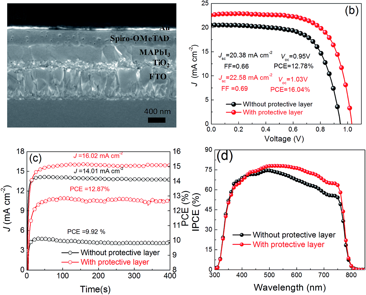 | ||
| Fig. 3 (a) Typical cross-sectional SEM images of a complete PSC fabricated with a protective layer during the annealing process. (b) J–V curves of the best PSCs fabricated from different annealing approaches. (c) The stabilized output at the maximum power point. (d) Typical IPCE spectra of the PSCs solar cells fabricated with and without protective layers. | ||
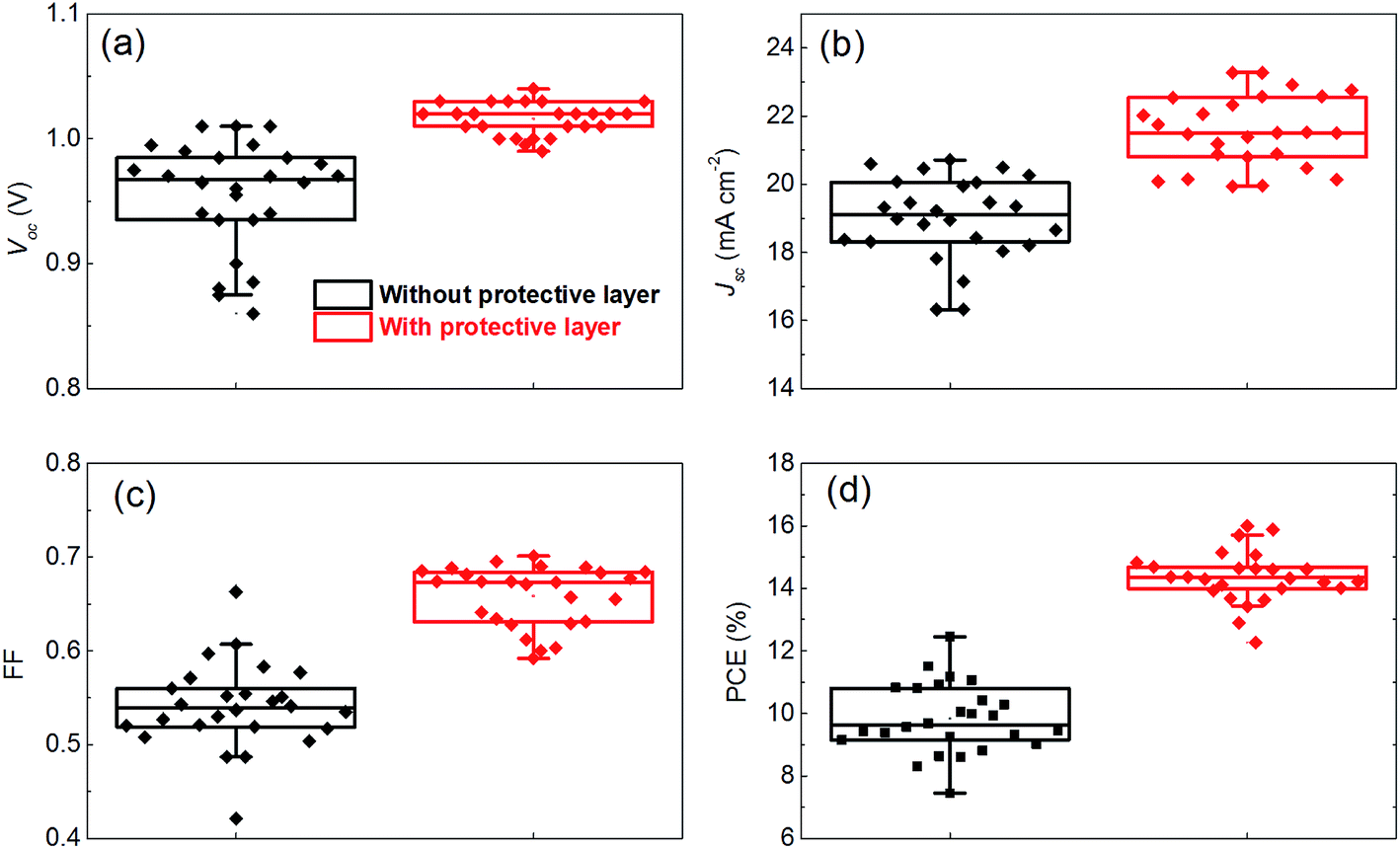 | ||
| Fig. 4 Box chart of photovoltaic parameters of a series PSCs extracted from J–V curves. (a) Voc, (b) Jsc, (c) FF, (d) PCE. | ||
Fig. 5a is Nyquist plots of impedance spectra for PSCs by employing a bias voltage of 0.9 V in dark. The simplified equivalent circuit is used to analysis the charge transportation and recombination in the PSCs.40–42 In this circuit, Rs is series resistance between two electrodes; charge transportation resistance (Rct) in parallel with a chemical capacity (CPEct) at high frequency, which ascribed to the perovskite–ETL and perovskite–HTL interface. The smaller value of Rct indicates better transportation of charges through those interface; recombination resistance (Rrec) in parallel with a chemical capacity (CPErec) at low frequency, which reflects the recombination information in PSCs. The recombination resistance (Rrec) is inversely related to the recombination rate of carriers,43 the larger value of Rrec indicates the less charge recombination in PSCs. The Rct of PSCs fabricated by employing protective layer during annealing process is 133.4 Ω, which is lower than the value 167.3 Ω obtained from the PSCs fabricated without protective layer. The reduced charge transportation resistance indicates more efficient charge transportation of carries in the whole devices. Meanwhile, the recombination resistance Rrec increased from 190.7 to 636.5 Ω when the protective layer was introduced during annealing process, the larger value of Rrec indicates the suppression of charge recombination due to the improvement of perovskite quality. The reduced recombination rate is beneficial to increase the FF and Voc of PSCs (see Fig. 3b).
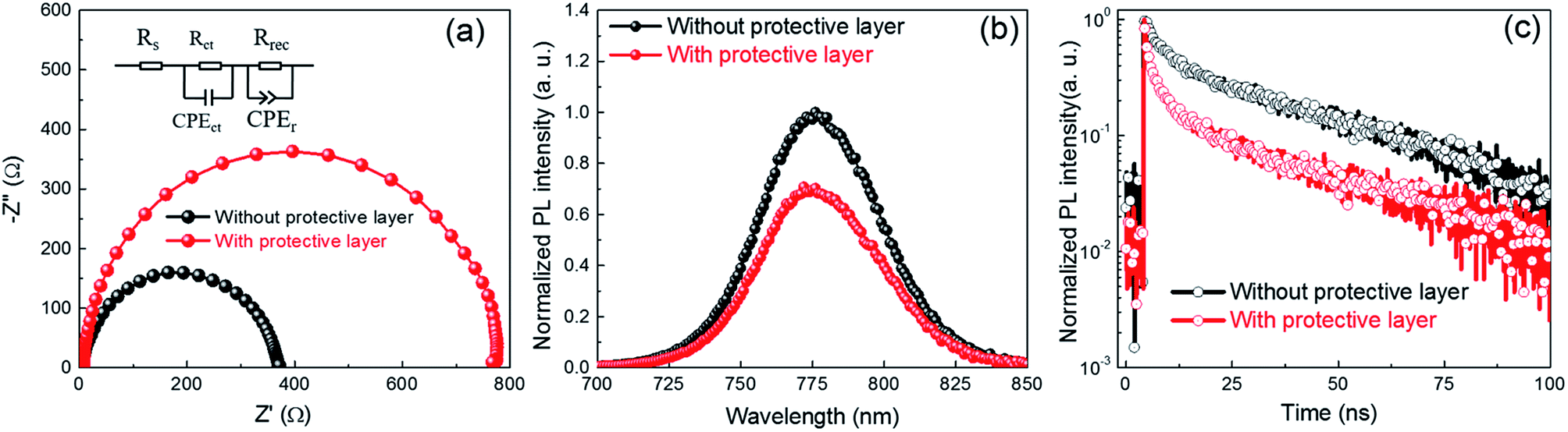 | ||
| Fig. 5 (a) Nyquist plots of the PSCs measured in dark under a bias voltage of 0.9 V. (b) Steady PL spectra of the MAPbI3 film annealed by different approaches. (c) Time resolved PL spectra and the fitting results by using bi-exponential decay. | ||
Fig. 5b are the normalized steady photo-luminescence (PL) spectra for studying the effects of perovskite quality on charge transfer at the interface of TiO2 and perovskite film. The sample for steady PL measurement is composed of FTO/TiO2/MAPbI3. Fig. 5b shows that a characteristic peak at 776 nm related the intrinsic bandgap (∼1.60 eV) of MAPbI3, which is consistent with the UV-Vis absorption spectra (see Fig. 2f). As comparison with the samples annealed without protective layer, the PL intensity of sampled annealed with protective layer deceases significantly, which indicates more efficient charge injection from MAPbI3 to TiO2 layers.44,45 The efficient charge extraction ability can be ascribed to the column-like grains (see Fig. 2d) and improved grain orientation (see Fig. 2e). The improved charge extraction ability and absorption ability in the range from 400 to 800 nm (see Fig. 2f) should be responsible for the increased Jsc obtained from PSCs (see Fig. 3b and 4b). Fig. 5c shows the time-resolved PL spectra of the perovskite film deposited on TiO2 substrates. The dynamic PL can be well fitted by a bi-exponential equation:
| I(t) = A1e−t/τ1 + A2e−t/τ2 |
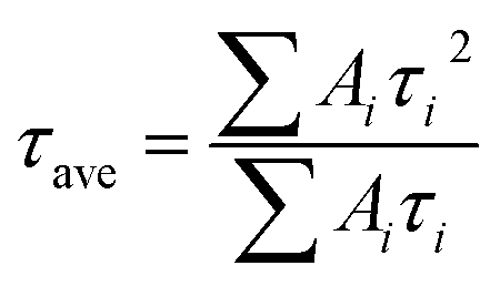
The average PL decay time reduced from 37.77 ns to 18.42 ns when the protective layer is employed during annealing process. The reduced τave also demonstrated that the efficient transportation and fast injection into TiO2 from perovskite film. The improved transportation and injection ability of charge can be ascribed to the less grain boundary along the thickness direction (see Fig. 2b and d). The reduced PL decay time is beneficial to reduce the combination at the interface at perovskite–ETL interface, which should be responsible for improvement in FF and Voc (see Fig. 3b). So higher Jsc of PSC fabricated with protective layer can be ascribed strong light harvest ability from 400 to 800 nm and fast injection of carriers. The higher Voc and FF can be ascribed to lower recombination rate due to less grains boundary in perovskite.
4. Conclusions
In summary, the solvent embedded in the perovskite precursor film play a key role in fabricating high quality perovskite films. It implies a solvent annealing effect during annealing of perovskite precursor film. We strengthen the intrinsic solvent annealing effects by pre-depositing a protective layer on the perovskite precursor film to retard the escape of solvent. The restricted solvent induces an obvious solvent annealing effect during annealing process. The strengthened solvent annealing effects lead to formation of high quality perovskite film with large grains and excellent grain orientation. The improved quality of perovskite film leads to efficient carrier transformation and injection, low recombination in devices. As a result, the performance of perovskite solar cells fabricated from corresponding perovskite film enhanced significantly. This work provides a facial method to obtain large grains by making use of self-embedded solvent in perovskite precursor film.Conflicts of interest
The authors declare no competing financial interest.Acknowledgements
This work was financially supported by Shenzhen Jiawei Photovoltaic Lighting Co. Ltd., and Tsinghua University Initiative Scientific Research Program (20161080165).References
- A. Kojima, K. Teshima, Y. Shirai and T. Miyasaka, J. Am. Chem. Soc., 2009, 131, 6050–6051 CrossRef CAS PubMed.
- W. S. Yang, B. W. Park, E. H. Jung, N. J. Jeon, Y. C. Kim, D. U. Lee, S. S. Shin, J. Seo, E. K. Kim, J. H. Noh and S. I. Seok, Science, 2017, 356, 1376–1379 CrossRef CAS PubMed.
- D. Bi, J. Luo, F. Zhang, A. Magrez, E. N. Athanasopoulou, A. Hagfeldt and M. Grätzel, ChemSusChem, 2017, 10, 1624–1630 CrossRef CAS PubMed.
- X. B. Cao, L. L. Zhi, Y. H. Li, F. Fang, X. Cui, Y. W. Yao, L. J. Ci, K. X. Ding and J. Q. Wei, J. Mater. Chem. C, 2017, 5, 7458–7464 RSC.
- Y. Zhang, L. Tan, Q. Fu, L. Chen, T. Ji, X. Hu and Y. Chen, Chem. Commun., 2016, 52(5), 674–5677 Search PubMed.
- X. B. Cao, C. L. Li, L. L. Zhi, Y. H. Li, X. Cui, Y. W. Yao, L. J. Ci and J. Q. Wei, J. Mater. Chem. A, 2017, 5, 8416–8422 CAS.
- C. G. Wu, C. H. Chiang, Z. L. Tseng, M. K. Nazeeruddin, A. Hagfeldt and M. Grätzel, Energy Environ. Sci., 2015, 8, 2725–2733 CAS.
- X. B. Cao, C. L. Li, Y. H. Li, F. Fang, X. Cui, Y. W. Yao and J. Q. Wei, Nanoscale, 2016, 8, 19804–19810 RSC.
- N. J. Jeon, J. H. Noh, W. S. Yang, Y. C. Kim, S. C. Ryu, J. W. Seo and S. I. Seok, Nature, 2015, 517, 476–480 CrossRef CAS PubMed.
- H. D. Kim, H. Ohkita, H. Benten and S. Ito, Adv. Mater., 2016, 28, 917–922 CrossRef CAS PubMed.
- C. H. Chiang and C. G. Wu, ChemSusChem, 2016, 9, 2666–2672 CrossRef CAS PubMed.
- W. Nie, H. Tsai, R. Asadpour, J. C. Blancon, A. J. Neukirch, G. Gupta, J. J. Crochet, M. Chhowalla, S. Tretiak, M. A. Alam, H. L. Wang and A. D. Mohite, Science, 2015, 347, 522–525 CrossRef CAS PubMed.
- M. Xiao, F. Huang, W. Huang, Y. Dkhissi, Y. Zhu, J. Etheridge, A. Gray-Weale, U. Bach, Y. B. Cheng and L. Spiccia, Angew. Chem., Int. Ed., 2014, 53, 9898–9903 CrossRef CAS PubMed.
- M. Yang, T. Zhang, P. Schulz, Z. Li, G. Li, D. H. Kim, N. Guo, J. J. Berry, K. Zhu and Y. Zhao, Nat. Commun., 2016, 7, 12305 CrossRef CAS PubMed.
- S. Bag and M. F. Durstock, ACS Appl. Mater. Interfaces, 2016, 8, 5053–5057 CAS.
- M. K. Kim, T. Jeon, H. I. Park, J. M. Lee, S. A. Nam and S. O. Kim, CrystEngComm, 2016, 18, 6090–6095 RSC.
- Z. Xiao, Q. Dong, C. Bi, Y. Shao, Y. Yuan and J. Huang, Adv. Mater., 2014, 26, 6503–6509 CrossRef CAS PubMed.
- D. Liu, L. Wu, C. Li, S. Ren, J. Zhang, W. Li and L. Feng, ACS Appl. Mater. Interfaces, 2015, 7, 16330–16337 CAS.
- J. Liu, C. Gao, X. He, Q. Ye, L. Ouyang, D. Zhuang, C. Liao, J. Mei and W. Lau, ACS Appl. Mater. Interfaces, 2015, 7, 24008–24015 CAS.
- Y. Numata, A. Kogo, Y. Udagawa, H. Kunugita, K. Ema, Y. Sanehira and T. Miyasaka, ACS Appl. Mater. Interfaces, 2017, 9, 18739–18747 CAS.
- N. J. Jeon, J. H. Noh, Y. C. Kim, W. S. Yang, S. Ryu and S. I. Seok, Nat. Mater., 2014, 13, 897–903 CrossRef CAS PubMed.
- Y. Rong, S. Venkatesan, R. Guo, Y. Wang, J. Bao, W. Li, Z. Fan and Y. Yao, Nanoscale, 2016, 8, 12892–12899 RSC.
- Y. Rong, Z. Tang, Y. Zhao, X. Zhong, S. Venkatesan, H. Graham, M. Patton, Y. Jing, A. M. Guloy and Y. Yao, Nanoscale, 2015, 7, 10595–10599 RSC.
- X. B. Cao, Y. H. Li, F. Fang, X. Cui, Y. W. Yao and J. Q. Wei, RSC Adv., 2016, 6, 70925–70931 RSC.
- X. Cao, L. Zhi, Y. Li, F. Fang, X. Cui, Y. Yao, L. Ci, K. Ding and J. Wei, ACS Appl. Mater. Interfaces, 2017, 9, 32868–32875 CAS.
- H. Zheng, W. Wang, S. Yang, Y. Liu and J. Sun, RSC Adv., 2016, 6, 1611–1617 RSC.
- S. Bae, S. J. Han, T. J. Shin and W. H. Jo, J. Mater. Chem. A, 2015, 3, 23964–23972 CAS.
- M. Long, T. Zhang, Y. Chai, C. F. Ng, T. C. W. Mak, J. Xu and K. Yan, Nat. Commun., 2016, 7, 13503 CrossRef CAS PubMed.
- J. Xu, A. Buin, A. H. Ip, O. Voznyy, R. Comin, M. Yuan, S. Jeon, Z. Ning, J. J. McDowell, P. Kanjanaboos, J. P. Sun, X. Lan, L. N. Quan, D. H. Kim, I. G. Hill, P. Maksymovych and E. H. Sargent, Nat. Commun., 2015, 6, 7081 CrossRef CAS PubMed.
- N. D. Marco, H. Zhou, Q. Chen, P. Sun, Z. Liu, L. Meng, E.-P. Yao, Y. Liu, A. Schiffer and Y. Yang, Nano Lett., 2016, 16, 1009–1016 CrossRef CAS PubMed.
- Y. Wang, J. Li, Q. Li, W. Zhu, T. Yu, X. Chen, L. Yin, Y. Zhou, X. Wang and Z. Zou, Chem. Commun., 2017, 53, 5032–5035 RSC.
- A. R. M. Yusoff and M. K. Nazeeruddin, J. Phys. Chem. Lett., 2016, 7, 851–866 CrossRef CAS PubMed.
- F. Hao, C. C. Stoumpos, P. Guo, N. Zhou, T. J. Marks, R. P. H. Chang and G. Kanatzidis, J. Am. Chem. Soc., 2015, 137, 11445–11452 CrossRef CAS PubMed.
- Y. Zhang, M. Liu, G. E. Eperon, T. C. Leijtens, D. McMeekin, M. Saliba, W. Zhang, M. Bastiani, A. Petrozza, L. M. Herz, M. B. Johnston, H. Lin and H. J. Snaith, Mater. Horiz., 2015, 2, 315–322 RSC.
- N. K. Noel, A. Abate, S. D. Stranks, E. S. Parrott, V. M. Burlakov, A. Goriely and H. J. Snaith, ACS Nano, 2014, 8, 9815–9821 CrossRef CAS PubMed.
- S. Bai, N. Sakai, W. Zhang, Z. Wang, J. T. W. Wang, F. Gao and H. J. Snaith, Chem. Mater., 2017, 29, 462–473 CrossRef CAS.
- J. W. Lee, H. S. Kim and N. G. Park, Acc. Chem. Res., 2016, 49, 311–319 CrossRef CAS PubMed.
- L. Li, Y. Chen, Z. Liu, Q. Chen, X. Wang and H. Zhou, Adv. Mater., 2016, 28, 9862–9868 CrossRef CAS PubMed.
- C. Sun, Y. Guo, B. Fang, J. Yang, B. Qin, H. Duan, Y. Chen, H. Li and H. Liu, J. Phys. Chem. C, 2016, 120, 12980–12988 CAS.
- S. Wang, W. Dong, X. Fang, Q. Zhang, S. Zhou, Z. Deng, R. Tao, J. Shao, R. Xia, C. Song, L. Hu and J. Zhu, Nanoscale, 2016, 8, 6600–6608 RSC.
- D. Liu, M. K. Gangishetty and T. L. Kelly, J. Mater. Chem. A, 2014, 2, 19873–19881 CAS.
- D. Yang, X. Zhou, R. Yang, Z. Yang, W. Yu, X. Wang, C. Li, S. Liu and R. P. H. Chang, Energy Environ. Sci., 2016, 9, 3071–3078 CAS.
- J. A. Christians, R. C. M. Fung and P. V. Kamat, J. Am. Chem. Soc., 2014, 136, 758–764 CrossRef CAS PubMed.
- H. S. Ko, J. W. Lee and N. G. Park, J. Mater. Chem. A, 2015, 3, 8808–8815 CAS.
- Q. Jiang, L. Zhang, H. Wang, X. Yang, J. Meng, H. Liu, Z. Yin, J. Wu, X. Zhang and J. You, Nat. Energy, 2016, 2, 16117 Search PubMed.
- D. Yang, R. Yang, X. Ren, X. Zhu, Z. Yang, C. Li and S. Liu, Adv. Mater., 2016, 28, 5206–5213 CrossRef CAS PubMed.
Footnote |
| † Electronic supplementary information (ESI) available. See DOI: 10.1039/c7ra10294a |
| This journal is © The Royal Society of Chemistry 2017 |