
 Open Access Article
 This Open Access Article is licensed under a Creative Commons Attribution-Non Commercial 3.0 Unported Licence
Direct growth of a graphitic nano-layer on optical fibers for ultra-fast laser application†
Conghao Yang‡
,
Ling Yun‡,
Yang Qiu,
Hanqing Dai ,
Detao Zhu,
Zhijia Zhu,
Zuxing Zhang*,
Kehan Yu* and
Wei Wei
,
Detao Zhu,
Zhijia Zhu,
Zuxing Zhang*,
Kehan Yu* and
Wei Wei
School of Optoelectronic Engineering, Nanjing University of Posts and Telecommunications, Nanjing 210023, China. E-mail: kehanyu@njupt.edu.cn; zxzhang@njupt.edu.cn; Fax: +86-25-85866296
First published on 10th November 2017
Abstract
Direct growth of graphitic nano-layer (GNL) on optical fiber is achieved using plasma-enhanced chemical vapor deposition. Clean and uniform GNL nanocrystalline flakes are grown in a controllable manner on the fiber-end without catalysts. 991 fs soliton pulse generation at 1559 nm is achieved using the GNL coated optical fiber in an erbium-doped fiber laser.
Two-dimensional (2D) layered materials, including graphene, topological insulators, transition metal dichalcogenides, and black phosphorus, have been attracting increasing attention in photonic and optoelectronic applications. In particular, graphene is a 2D honeycomb lattice structure of carbon atoms characterized by a linear relation between energy and momentum, massless Dirac fermions, broad wavelength range and ultrafast relaxation mechanism, making it a promising saturable absorber (SA) for ultra-fast lasers.1–4 Several techniques have been developed for the fabrication of graphene-based saturable absorbers (GSAs), e.g. mechanical exfoliation,5,6 liquid phase exfoliation,7–9 chemical vapor deposition (CVD),10–13 graphene oxide (GO),9,14 and reduced GO.14,15 However, the existing methods of preparing GSAs usually suffer from complex procedure, residual polymer and metal catalysts, and mechanical damage.16 In addition, many reported GSAs are based on graphene/polymer composites or stacks,2,11,17 whereas the low optical damage threshold of the polymer could severely limit the output power of the laser. Therefore, a feasible, reproducible, and controllable technique is highly desired for the fabrication of GSA.
Plasma-enhanced chemical vapor deposition (PECVD) has emerged as an important method for producing carbon materials such as diamonds, carbon nanotubes and vertically-oriented graphene (VG) nanosheets as well as graphene.18–22 The energetic electrons generated by the plasma boost the ionization, excitation and dissociation of hydrocarbon precursors at relatively low temperature. Therefore, graphene can be growth directly on the desired substrates at low temperature by PECVD without metal catalysts. PECVD growth of graphene or VG has been conducted on virtually any substrates ranging from macro-sized planar23–26 and cylindrical shapes to millimeter-,27 micrometer-,28 and even nanometer-sized29 structures. This ability allows the easy fabrication of different graphene-based devices for diverse applications.
Here, we report a one-step fabrication of graphitic nano-layer saturable absorber (GNLSA) on optical fiber-end by PECVD. By changing growth time, desired layer number of graphitic nano-layer (GNL) can be uniformly grown on the optical fiber-end. The fabricated GNLSA was used to mode-lock an erbium-doped fiber (EDF) laser. The generated optical soliton pulses with the 991 fs duration and 2.7 nm bandwidth was centered at 1559 nm. The as-prepared GNLSA can operation stably at mode locking state with the maximum pump power of 700 mW. The reported method enables a feasible, reproducible, and controllable technique for the fabrication of GSA.
Single-mode fibers (SMFs) were stripped, wiped up with alcohol, cut by fiber cleaver. Then fiber ends were cleaned by an arc discharge (Fusion Splicer). Fused quartz slides (1.5 × 1.5 cm2, 1 mm in thickness), used as reference substrates, were cleaned in ultrasonic bathes of acetone and isopropanol, sequentially. Then they were rinsed with deionized water, dried in nitrogen flow.
GNL was produced using a radio-frequency (rf) PECVD system consisting of a tube furnace (OTF-1200X) and a rf generator (VERG-500 RF POWER GENERATOR, f = 13.56 MHz). The SMF and the fused quartz slide were placed side by side on a home-made graphite holder at the center of the heating area. The reaction chamber was evacuated to ∼40 mTorr, then a mixture of 1 standard cubic centimeter per minute (sccm) of methane (CH4) and 9 sccm of hydrogen (H2) were introduced into the system when the reactor was heated up to 700 °C. The GNL growth was conducted at ∼300 mTorr, with rf power of 200 W for 40 min. After the growth, the CH4 flow, H2 flow, and plasma were switched out; the reactor was cooled down in an argon (Ar) flow.
The morphology of GNL grow on fiber-end was observed using a field-emission SEM (Hitachi S4800). Raman spectroscopy was carried out with an EZRaman-M Portable Raman System (EZM-785-A2, λ = 532 nm). The crystal structure of GNL was analyzed by a Bruker D8 polycrystalline X-ray diffraction (D/MAX-2500, λ = 1.5406 Å). Optical transmittance of GNL was tested with a PerkinElmer Lambda 950 machine. The laser performance was characterized by an optical spectrum analyzer (Yokogawa, AQ6370D), a Serial Data Analyzer Oscilloscope (LeCroy, SDA-6000A), a 10 GHz photo-detector (KG-PD-10G), a FROG Scan (Mesaphotonics), and a 30 GHz RF spectrum analyzer (RS-FSV30).
By PECVD, GNL was uniformly grown on the optical fiber-end (SMF, 125 μm in diameter), as observed under SEM (Fig. 1a). The morphology of the GNL from the core area to the edge area of the fiber-end, as shown in Fig. 1b–d, is featured by nano-platelets. No VG was observed under the present condition of growth.
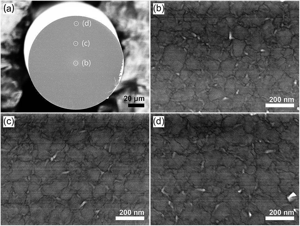 | ||
| Fig. 1 (a) SEM image of a fiber-end with directly grown GNL. (b)–(d) SEM images taken from the positions of the fiber-end marked in (a). | ||
Nanocrystalline nature of the as-grown GNL was revealed by Raman scattering spectrum. Three distinct peaks were observed at 1348 cm−1 (D band), 1584 cm−1 (G band) and 2695 cm−1 (2D band), as shown in Fig. 2a. The G and 2D band are the Raman characteristic peaks of sp2-hybridized carbon–carbon bonds in graphene,30,31 indicating the formation of graphitized structure. The D band together with 2D′ band (3241 cm−1) is attributed to the structural disorder in the GNL.23 The small 2D′ band reflects the existence of the D′ band that is probably convoluted with the G band. The intense D band reveals small crystalline with numerous open edges and defects in the as-grown GNL. The fraction of sp2 carbon in the as-grown GNL is imperfect, which is consistent with reported results.26,32,33 Additionally, the X-ray diffraction (XRD) (002) peak at 2θ = 26.543° is corresponding to an interlayer spacing d002 = 0.335 nm (Fig. 2b), which is very close to that of pristine few-layer graphene.
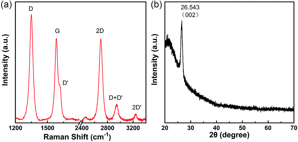 | ||
| Fig. 2 (a) Raman scattering spectrum and (b) XRD pattern of GNL on quartz substrate. | ||
The graphene film growth in PECVD is involved with two steps: (a) nucleation: in the early growth stage, precursor (e.g. CH4) is dissociated into various reactive radicals in plasma, the carbon-related radicals deposited onto the substrate to form graphene islands; (b) growth: with the continuous growth, higher density of graphene islands form and coalesce into a continuous and uniform graphene films.18,34 With increasing the growth time, the layer number of graphene increased, from few-layer graphene to multilayer graphene, and eventually graphitic layer can be obtained.
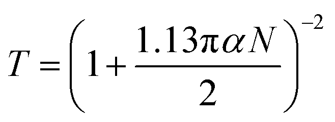
The linear transmission spectrum of the as-grown GNL is nearly featureless from 200 to 2400 nm, and with a peak in the ultraviolet region at around 270 nm (Fig. 3a), which is consistent with graphene made by other techniques.35 The number of layers of GNL can be evaluated by a formula36
 | (1) |
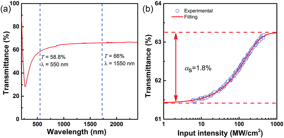 | ||
| Fig. 3 (a) Transmittance spectrum of an as-grown GNL thin film on quartz substrate. (b) Transmittance of the GNLSA as a function of average pump power. | ||
Using a typical twin-detector measurement technology, the nonlinear saturable absorbance property of GNLSA was investigated. The illumination pulse was characterized by a nanotube mode-locked fiber laser delivering ∼600 fs pulse with 23 MHz repetition rate at 1550 nm. As illustrated in Fig. 3b, the as-prepared GNLSA exhibits typical feature of saturable absorption, i.e. the light transmission increases with the pulse intensity. The experimental data are fitted through the two-level saturable model
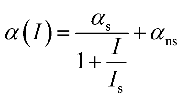 | (2) |
![[thin space (1/6-em)]](https://www.rsc.org/images/entities/char_2009.gif) :H2 ratio and growth temperature.20 It worth noting that the modulation depth of a GSA is controlled by the layer number of graphene. For example, multi-layer graphene/PMMA stacks can provide the desired modulation depth.11 The direct growth of GNL proposed here greatly simply the fabrication procedure, avoiding the complicate and time consuming growth and post transfer processes.
:H2 ratio and growth temperature.20 It worth noting that the modulation depth of a GSA is controlled by the layer number of graphene. For example, multi-layer graphene/PMMA stacks can provide the desired modulation depth.11 The direct growth of GNL proposed here greatly simply the fabrication procedure, avoiding the complicate and time consuming growth and post transfer processes.
We constructed an EDF laser to investigate the performance of as-prepared GNLSA. As shown in Fig. 4. The laser system consisted of a wavelength division multiplexer (WDM), a 5 m EDF with 6 dB m−1 absorption at 980 nm, an optical coupler (OC) with output ratio of 10%, a polarization-independent isolator (PI-ISO), a GNL mode-locker, and a polarization controller (PC). The mode-locker is achieved by insert GNLSA into a bare fiber adapter and connect with a fiber adapter by flange (inset of Fig. 4). The dispersion parameters for EDF and SMF are about −16 ps (nm km)−1 and 17 ps (nm km)−1, respectively. The total cavity length is ∼24 m and the net dispersion is ∼−0.31 ps2.
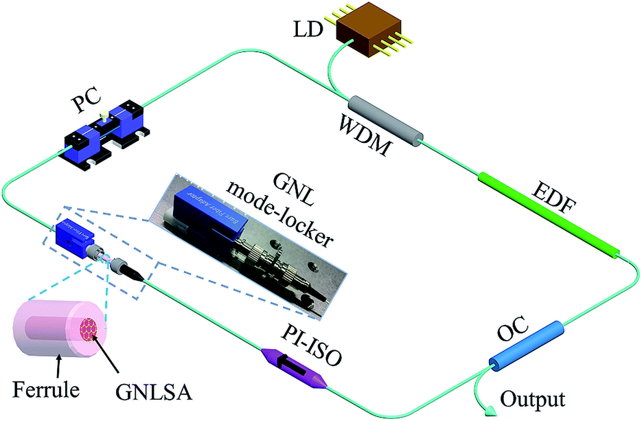 | ||
| Fig. 4 Schematics of mode-locked fiber laser. Inset: a GNL mode-locker. | ||
The threshold pump power for continuous wave lasing was about 50 mW. Fig. 5 summarizes the characteristics of mode-locked with the pump power of 200 mW. A mode-locked laser spectrum centering at 1559 nm is shown in Fig. 5a, with a 3 dB spectral bandwidth of 2.7 nm. Kelly sidebands at the spectrum shoulders, confirming typical soliton-like pulse formations, originated from intracavity periodic perturbations.2,39 The autocorrelation trace is illustrated in Fig. 5b, and the pulse duration of 991 fs is given by sech2 fitting. The time-bandwidth product of 0.33 is close to the value of the transform-limited sech2-shaped pulses.17 The repetition period of the output pulses train was ∼118 ns, corresponding to the cavity round-trip time (Fig. 5c). The repetition rate of the fundamental cavity frequency of 8.449 MHz together with a radio frequency (RF) spectrum signal-to-noise ratio of ∼58 dB are shown in Fig. 5d indicating a laser operation in low-amplitude fluctuations and stability mode-locking regime.40,41 No spectrum modulation was observed over 1 GHz (inset of Fig. 5d), indicating no Q-switching instabilities.40,42 The investigations of the growth condition without the rf power are available in ESI.†
 | ||
| Fig. 5 Mode-locking characteristics. (a) Optical spectrum, (b) autocorrelation trace, (c) pulse train, (d) RF spectrum. Inset: wideband RF spectrum up to 1 GHz. | ||
An inherent characteristic of the proposed SA is the high optical damage threshold. The mode locking operation worked from the self-started threshold to the maximum available pump power of 700 mW. Fig. 6 shows the average output power and central wavelength as a function of pump power for GNLSA, respectively. The average output power increases linearly as the pump power increasing; the central wavelength almost keeps constant, and none output power drop is observed, indicating a robust GNLSA resistant to thermal damage. The inset in Fig. 6 shows the optical spectrum of stable soliton mode locking by increasing the pump power to 700 mW.
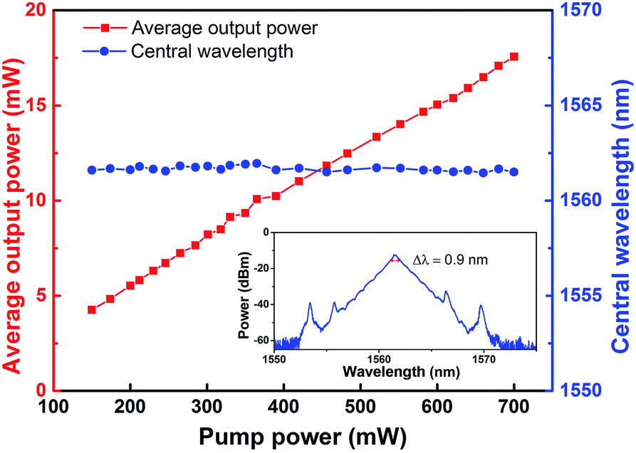 | ||
| Fig. 6 Average output power and central wavelength versus pump power at the mode-locking operation state. Inset: spectrum at pump power of 700 mW. | ||
It is worthwhile noting that the VG can be grown on optical fiber-ends with a fast growth, e.g. PECVD at higher temperature. But no mode-locked laser was obtained using a VG coated optical fiber. Calculated with eqn (1), the VG is equivalent to a 32-layered GNL. The insertion loss of VG is perhaps too high to output mode-locked laser. The SEM images of VG grown on optical fiber-end are available in ESI.†
In conclusion, we report a one-step fabrication of GNLSA on optical fiber-end for passively mode-locked laser by PECVD. Without catalyst, nanocrystalline GNL with controllable number of layers was uniformly grown on the optical fiber-end, exhibiting a modulation depth of 1.8% with a 23-layered GNLSA. A stable mode-locked fiber laser was achieved using a 23-layered GNLSA with spectrum centered at 1559 nm, 3 dB bandwidth of 2.7 nm, soliton pulses of 991 fs, and repetition rate of 8.449 MHz. The as-grown GNLSA can bear pump power up to 700 mW, the average output power reached 17.6 mW. This feasible, clean and controllable fabrication approach may greatly facilitate the development of the fabrication of graphene based devices.
Conflicts of interest
There are no conflicts to declare.Acknowledgements
This work was financially supported by the National Natural Science Foundation of China No. 61504064, the Natural Science Foundation of Jiangsu Province, China (No. BK20150847 and No. BK20161521), and NUPTSF Grant no. NY214137 and no. NY214002.References
- Q. Bao, H. Zhang, Y. Wang, Z. Ni, Y. Yan, Z. X. Shen, K. P. Loh and D. Y. Tang, Adv. Funct. Mater., 2009, 19, 3077–3083 CrossRef CAS.
- Z. Sun, T. Hasan, F. Torrisi, D. Popa, G. Privitera, F. Wang, F. Bonaccorso, D. M. Basko and A. C. Ferrari, ACS Nano, 2010, 4, 803–810 CrossRef CAS PubMed.
- Z. Sun, T. Hasan and A. C. Ferrari, Phys. E, 2012, 44, 1082–1091 CrossRef CAS.
- A. Martinez and Z. Sun, Nat. Photonics, 2013, 7, 842–845 CrossRef CAS.
- Y. M. Chang, H. Kim, J. H. Lee and Y.-W. Song, Appl. Phys. Lett., 2010, 97, 211102 CrossRef.
- A. Martinez, K. Fuse and S. Yamashita, Appl. Phys. Lett., 2011, 99, 121107 CrossRef.
- F. Bonaccorso and Z. Sun, Opt. Mater. Express, 2014, 4, 63–78 CrossRef.
- D. Popa, Z. Sun, F. Torrisi, T. Hasan, F. Wang and A. C. Ferrari, Appl. Phys. Lett., 2010, 97, 831–833 CrossRef.
- Q. Bao, H. Zhang, J. X. Yang, S. Wang, D. Y. Tang, R. Jose, S. Ramakrishna, C. T. Lim and K. P. Loh, Adv. Funct. Mater., 2010, 20, 782–791 CrossRef CAS.
- H. Zhang, D. Y. Tang, R. J. Knize, L. Zhao, Q. Bao and K. P. Loh, Appl. Phys. Lett., 2010, 96, 111112 CrossRef.
- G. Sobon, J. Sotor, I. Pasternak, A. Krajewska, W. Strupinski and K. M. Abramski, Opt. Mater. Express, 2015, 5, 2884–2894 CrossRef CAS.
- H. Zhang, D. Y. Tang, L. Zhao, Q. Bao and K. P. Loh, Opt. Express, 2009, 17, 17630–17635 CrossRef CAS PubMed.
- G. Zhu, X. Zhu, F. Wang, S. Xu, Y. Li, X. Guo, K. Balakrishnan, R. A. Norwood and N. Peyghambarian, IEEE Photonics Technol. Lett., 2016, 28, 7–10 CrossRef CAS.
- Y.-W. Song, S.-Y. Jang, W.-S. Han and M.-K. Bae, Appl. Phys. Lett., 2010, 96, 051122 CrossRef.
- H. Zhang, Q. Bao, D. Y. Tang, L. Zhao and K. P. Loh, Appl. Phys. Lett., 2009, 95, 141103 CrossRef.
- F. Bonaccorso, A. Lombardo, T. Hasan, Z. Sun, L. Colombo and A. C. Ferrari, Mater. Today, 2012, 15, 564–589 CrossRef CAS.
- Z. Sun, D. Popa, T. Hasan, F. Torrisi, F. Wang, E. J. R. Kelleher, J. C. Travers, V. Nicolosi and A. C. Ferrari, Nano Res., 2010, 3, 653–660 CrossRef CAS.
- M. Li, D. Liu, D. Wei, X. Song, D. Wei and A. T. S. Wee, Adv. Sci., 2016, 3, 1600003 CrossRef PubMed.
- Z. Bo, S. Mao, Z. J. Han, K. Cen, J. Chen and K. Ostrikov, Chem. Soc. Rev., 2015, 44, 2108–2121 RSC.
- Z. Bo, Y. Yang, J. Chen, K. Yu, J. Yan and K. Cen, Nanoscale, 2013, 5, 5180–5204 RSC.
- K. Ostrikov, Rev. Mod. Phys., 2005, 77, 489–511 CrossRef CAS.
- K. Ostrikov and A. B. Murphy, J. Phys. D: Appl. Phys., 2007, 40, 2223–2241 CrossRef CAS.
- K. Yu, Z. Bo, G. Lu, S. Mao, S. Cui, Y. Zhu, X. Chen, R. S. Ruoff and J. Chen, Nanoscale Res. Lett., 2011, 6, 202–210 CrossRef PubMed.
- H. Bi, S. Sun, F. Huang, X. Xie and M. Jiang, J. Mater. Chem., 2012, 22, 411–416 RSC.
- Y. S. Kim, K. Joo, S.-K. Jerng, J. H. Lee, D. Moon, J. Kim, E. Yoon and S.-H. Chun, ACS Nano, 2014, 8, 2230–2236 CrossRef CAS PubMed.
- L. Zhang, Z. Shi, Y. Wang, R. Yang, D. Shi and G. Zhang, Nano Res., 2011, 4, 315–321 CrossRef CAS.
- Z. Bo, K. Yu, G. Lu, S. Cui, S. Mao and J. Chen, Energy Environ. Sci., 2011, 4, 2525–2528 CAS.
- H.-C. Chang, H.-Y. Chang, W.-J. Su, K.-Y. Lee and W.-C. Shih, Appl. Surf. Sci., 2012, 258, 8599–8602 CrossRef CAS.
- K. Yu, G. Lu, Z. Bo, S. Mao and J. Chen, J. Phys. Chem. Lett., 2011, 2, 1556–1562 CrossRef CAS.
- A. C. Ferrari, J. C. Meyer, V. Scardaci, C. Casiraghi, M. Lazzeri, F. Mauri, S. Piscanec, D. Jiang, K. S. Novoselov, S. Roth and A. K. Geim, Phys. Rev. Lett., 2006, 97, 187401 CrossRef CAS PubMed.
- D. Graf, F. Molitor, K. Ensslin, C. Stampfer, A. Jungen, C. Hierold and L. Wirtz, Nano Lett., 2006, 7, 238–242 CrossRef PubMed.
- T. E. Benavidez, R. Martinez-Duarte and C. D. Garcia, Anal. Methods, 2016, 8, 4163–4176 RSC.
- X. Chen, B. Wu and Y. Liu, Chem. Soc. Rev., 2016, 45, 2057–2074 RSC.
- W. Yang, C. He, L. Zhang, Y. Wang, Z. Shi, M. Cheng, G. Xie, D. Wang, R. Yang, D. Shi and G. Zhang, Small, 2012, 8, 1429–1435 CrossRef CAS PubMed.
- F. Bonaccorso, Z. Sun, T. Hasan and A. C. Ferrari, Nat. Photonics, 2010, 4, 611–622 CrossRef CAS.
- S. E. Zhu, S. Yuan and G. C. A. M. Janssen, Europhys. Lett., 2014, 108, 17007–17010 CrossRef.
- R. R. Nair, P. Blake, A. N. Grigorenko, K. S. Novoselov, T. J. Booth, T. Stauber, N. M. R. Peres and A. K. Geim, Science, 2008, 320, 1308 CrossRef CAS PubMed.
- L. Li, S. Jiang, Y. Wang, X. Wang, L. Duan, D. Mao, Z. Li, B. Man and J. Si, Opt. Express, 2015, 23, 28698–28706 CrossRef CAS PubMed.
- M. L. Dennis and I. N. Duling, IEEE J. Quantum Electron., 1994, 30, 1469–1477 CrossRef CAS.
- F. Wang, A. G. Rozhin, V. Scardaci, Z. Sun, F. Hennrich, I. H. White, W. I. Milne and A. C. Ferrari, Nat. Nanotechnol., 2008, 3, 738–742 CrossRef CAS PubMed.
- D. Von der Linde, Appl. Phys. B, 1986, 39, 201–217 CrossRef.
- U. Keller, K. J. Weingarten, F. X. Kärtner, D. Kopf, B. Braun, I. D. Jung, R. Fluck, C. Hönninger, N. Matuschek and J. A. D. Au, IEEE J. Sel. Top. Quantum Electron., 1996, 2, 435–453 CrossRef CAS.
Footnotes |
| † Electronic supplementary information (ESI) available: The investigations of the growth condition without the rf power and the SEM images of VG. See DOI: 10.1039/c7ra10260g |
| ‡ These authors contributed equally to this work. |
| This journal is © The Royal Society of Chemistry 2017 |