
 Open Access Article
 This Open Access Article is licensed under a Creative Commons Attribution-Non Commercial 3.0 Unported Licence
Efficiency enhancement in inverted planar perovskite solar cells by synergetic effect of sulfated graphene oxide (sGO) and PEDOT:PSS as hole transporting layer†
Heng Guoa,
Xu Huanga,
Bingxue Pua,
Jian Yanga,
Haiyuan Chena,
Yajun Zhoua,
Jin Yanga,
Yulan Lia,
Zhiming Wangb and
Xiaobin Niu *ab
*ab
aState Key Laboratory of Electronic Thin Film and Integrated Devices, University of Electronic Science and Technology of China, Chengdu 610054, China. E-mail: xbniu@uestc.edu.cn
bInstitute of Fundamental and Frontier Science, University of Electronic Science and Technology of China, Chengdu 610054, China
First published on 30th October 2017
Abstract
Inverted planar perovskite solar cells (PSCs) exhibiting a high power conversion efficiency (PCE) have mainly been demonstrated by using poly(3,4-ethylenedioxythiophene):poly(styrenesulfonate) (PEDOT:PSS) as the hole transport layer (HTL). As an alternative to the PEDOT:PSS, graphene oxide (GO) is also employed as a HTL in PSCs with decent PCEs. However, the strong acidity and hygroscopicity of PEDOT:PSS and insulting property of GO were the major factors for hindering the fabrication of high-performance PSCs. Here, we demonstrated sulfated graphene oxide (sGO) as a HTL replacing the conventionally used GO and PEDOT:PSS in PSCs, but pristine sGO as simple HTL cannot improve photovoltaic performance of PSCs with a maximum efficiency of 9.9%. Hence, we report a simple solution route for preparing a sGO–PEDOT:PSS composite HTL by combining solution-processable sGO with commercialized PEDOT:PSS solution. The PSC fabricated with 1![[thin space (1/6-em)]](https://www.rsc.org/images/entities/char_2009.gif) :1 sGO–PEDOT:PSS HTL shows a dramatically enhanced PCE of 13.9%, versus 11.5% for PSC with pristine PEDOT:PSS HTL. This promising strategy could be a critical step toward the ideal HTL design for the advancement of practical perovskite solar cells.
:1 sGO–PEDOT:PSS HTL shows a dramatically enhanced PCE of 13.9%, versus 11.5% for PSC with pristine PEDOT:PSS HTL. This promising strategy could be a critical step toward the ideal HTL design for the advancement of practical perovskite solar cells.
1. Introduction
In the space of a few years, state-of-the-art power conversion efficiency (PCE) based on organometal trihalides perovskite photovoltaic devices (OTPV) has been dramatically improved from 3.8% up to 22.1%.1–5 Various lead halide perovskite solar cells (PSCs) use either mesoporous structure (MS) or planar heterojunction (PHJ) with n–i–p or p–i–n layout.6,7 Regardless of the cell architecture, the perovskite absorber layer is sandwiched between electron transport layer (ETL) and hole transport layer (HTL). Upon the light absorption of incident photons, carriers generated in perovskites travel, separate and gather through a transport pathway including the ETL or HTL, the collector electrodes, and interfaces in between.8 Undoubtedly, the PCE could be further improved by materials design and structure optimization.9,10 So far, the record top-performing perovskite-based solar cells usually employ mesostructured titanium dioxide (TiO2) as ETL in the mesoscopic type devices,11 which presents a very promising photovoltaic performance with great potential in real applications. However, the desired high processing temperature (>450 °C)12,13 of compact or mesoporous TiO2 increases the fabrication cost and manufacturing difficulty. Additionally, the relative high cost of 2,2′-7,7′-tetrakis(N,N-di-p-methoxyphenylamine)-9,9′-spirobifluorene (spiro-OMeTAD) as HTL along with the need of using high quality dopants and stability risks also prevents the use of flexible substrates and limits the further development of perovskite solar cells.14–16To overcome these drawbacks, inverted planer heterojunction PSCs with a layered structure of indium tin oxide (ITO)/HTL/perovskite/ETL/electrode have been developed with promising efficiencies over 15%.17,18 Since then, inverted PSCs were demonstrated to have an efficiency comparable with the mesoscopic type devices. Because these HTLs can be solution-processed easily, they can be fabricated by low-temperature annealing, and have a simple planar device structure.19 Among several conductive polymers used as the HTLs, poly(3,4-ethylenedioxythiophene):poly(styrenesulfonate) (PEDOT:PSS) is a famous and acknowledged available water soluble conductive polymer used as anode interfacial material for optoelectronic organic devices.20,21 More recently, several desirable properties, such as high mechanical flexibility, good thermal stability and high transparency in the visible range,22 also make PEDOT:PSS film a suitable candidate for the HTL application in perovskite solar cells.23,24 But, pristine PEDOT:PSS still suffers from a very low conductivity and inhomogeneous electrical properties. Moreover, PEDOT:PSS can cause degradation of the device and reduce the device durability because of the detrimental effects of its strong acidity (pH ∼ 1) and hygroscopicity.25 Additionally, other drawbacks of PEDOT:PSS, if compared to inorganic material layers (e.g. NiOx, WO3, ZnO, Al2O3, TiO2),26 are the tricky control of the perovskite deposition onto a soft polymeric surface and relatively smaller open circuit voltage (Voc) values of PSCs.27
To address this problem, graphene oxide (GO), as an effective alternative for PEDOT:PSS in organic and hybrid photovoltaic solar cells, has attracted significant research interests due to its low production costs and good dispersibility in many solvents.28–32 Furthermore, GO can be easily produced from graphene through chemical oxidation.33,34 However, GO has the primary disadvantage for HTLs such as hygroscopic and electrically insulting properties.35,36 Then, the efforts to develop GO derivatives have mostly focused on high work function and high conductivity, which makes them excellent supporters to satisfy most of the requirements of an ideal hole- and electron-extraction layers in PSCs.37 Among these GO derivatives, reduced GOs are attracting more and more interests, which are obtained by reduction reaction with the removal of oxygenous groups and the addition of the edge functionalization.38,39 However, several reduced GOs still suffer from low dispersion concentration and irreversible agglomeration.
Benefiting from these findings, here we demonstrated that sulfated graphene oxide (sGO)40 with –SO3H groups can serve as a hole extraction material to replace the conventional used GO and PEDOT:PSS in inverted planar PSCs. In this regard, the PSCs based on sGO HTL showed better device efficiencies (a maximum PCE of 9.9%) than those of the reference device using GO HTL (a maximum PCE of 6.7%). Contrarily, the PSCs fabricated with PEDOT:PSS HTL exhibit a maximum PCE (11.5%) by more than 13% compared with the sGO HTL-based PSCs. These results revealed the potentiality of sGO as HTL for the up scaling of PSCs-based technology. Subsequently, we combined solution-processable sGO with commercialized PEDOT:PSS solution, and systemically studied the synergetic effects of the sGO–PEDOT:PSS as a new composite HTL. We find that the resulting sGO–PEDOT:PSS composite HTLs can complement the drawbacks of pristine PEDOT:PSS and pure sGO. By applying such an efficient HTL, a planar device configuration of glass/ITO/sGO–PEDOT:PSS/PCBM/Ag results in a dramatically enhanced Voc of 1.01 V and a relatively high short-circuit current (Jsc) of 19.4 mA cm−2, corresponding to a maximum PCE of 13.9%. The typical PCE of PSCs achieved with high reproducibility was improved by 21% compared to that of PSCs with pristine PEDOT:PSS HTL.
2. Experimental
2.1. Synthesis of sGO
Sulfated graphene oxide (sGO) was prepared from graphene oxide (GO, purity > 99 wt%, layers: <3, diameter: 0.5–3.0 μm, Chengdu Organic Chemicals Co. Ltd.) powder according to the reported procedure with some modifications.40 A simplified sketch of the synthetic process involving the preparation of sGO powders from GO powders is shown in Fig. 1. In more detail, GO (200 mg) was placed into a 60 mL of fuming sulphuric acid (H2SO4, 98%, Alfa Aesar). The reaction mixture was stirred at room temperature for 72 h under N2 atmosphere to obtain a dark brown suspension. It was then added dropwise into a flask containing diethyl ether (40 mL, anhydrous, Alfa Aesar) with vigorous stirring in an ice bath. The mixture was then allowed to settle and decant. The precipitates were separated from solution through centrifugation. The obtained solid was then purified by repeated centrifugation and redispersed in diethyl ether. Finally, the resulting dark sGO solid was dried in a vacuum oven at 60 °C for 72 h before use.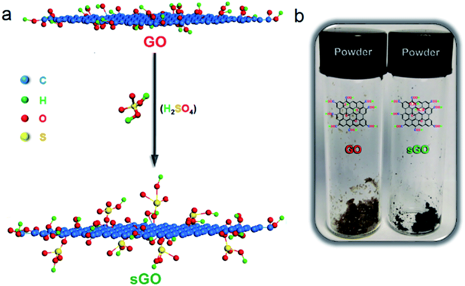 | ||
| Fig. 1 (a) Schematic illustration of the sGO preparation procedures. (b) Photograph of GO and sGO powders. | ||
2.2. Synthesis of CH3NH3I
Methylammonium iodide (CH3NH3I, MAI) was synthesized according to previous studies.41 Briefly, 38 mL HI solution (HI, 57 wt% in water, Alfa Aesar) and 34 mL methylamine solution (CH3NH2, 33 wt% in absolute ethanol, Alfa Aesar) were mixed in a 150 mL three-necked flask at 0 °C for 2 h in an ice-water bath. The HI solution was added dropwise while stirring. After the reaction, the resulting mixtures were rotary evaporated at 50 °C for 1 h to remove the solvent, and then the resulting powder was recovered by precipitation. The precipitate was washed with diethyl ether and then recrystallized in ethanol. This step was repeated three times, and then finally the MAI powder was dried at 60 °C overnight in a vacuum oven. To prepare the perovskite precursor solution, MAI and lead(II) iodide (PbI2, 99% purity, Aldrich) powder at 1:1 molar ratio were mixed in anhydrous dimethylformamide (DMF, anhydrous, 99.8%, Sigma-Aldrich) with a concentration of 1.5 M. Then the final solution was vigorous stirred overnight at 60 °C in a glovebox and filtered with a 0.22 μm PTFE filter before use.
2.3. HTL preparation
The GO or as-synthesized sGO were added into deionized water to form the GO or sGO solution with a concentration of 1.0 mg mL−1 under ultrasonic bath treatment. Then, GO/PEDOT:PSS solution was prepared by mixing GO solution and PEDOT:PSS (Clevios™ PVP. AI 4083, Heraeus Materials Technology Shanghai Ltd.) solution at 1:1 equi-volume ratio at room temperature, magnetically stirred for 72 h and filtered by polytetrafluoroethylene (PTFE) filters (2 μm) before use. Meanwhile, the as-prepared sGO solution was added into PEDOT:PSS solution with volume ratios of 1:2, 1:1, and 2:1, respectively, forming the resultant sGO/PEDOT:PSS solution. Thin films of GO, sGO, PEDOT:PSS (PEDOT), GO/PEDOT:PSS (1:1 GO–PEDOT) and sGO/PEDOT:PSS (1:2 sGO–PEDOT, 1:1 sGO–PEDOT, and 2:1 sGO–PEDOT) were spin-coated from the corresponding solutions onto patterned ITO/glass (1.5 × 1.5 cm2, 7 Ω sq−1, Zhuhai Kaivo Co., Ltd) substrates at 4000 rpm for 25 s in air at room temperature, followed by thermal treatment at 150 °C for 15 min.
2.4. Device fabrication
ITO-coated glass substrates were cleaned sequentially by sonication in detergents, de-ionized water, acetone, ethanol, and isopropanol for 15 min each. The substrates were dried by clean nitrogen stream, followed by an UV-ozone treatment for 15 min. The HTL layers were spin-coated onto clean ITO substrates through spin-coating process as mentioned above. The films were then transferred into a nitrogen-filled glovebox (both H2O and O2 < 0.1 ppm). Next, these CH3NH3PbI3 perovskite films were formed by spin coating perovskite precursor solutions at 4000 rpm for 35 s. During this procedure, 100 μL of chlorobenzene was pipetted onto the spinning substrate after 12 s. Thereafter, the substrate was put onto a hotplate and covered by a glass Petri dish for 1 h at 100 °C. After cooling down to room temperature, the PC61BM (a 20 mg mL−1 chlorobenzene solution) as an ETL was deposited by spin coating at 2000 rpm for 60 s. Finally, the devices were finished by the thermal evaporation 120 nm Ag as electrode under high vacuum (∼10−6 torr, at a rate of ∼1.0 Å s−1) through a shadow mask. The device area is 0.13 cm2.2.5. Characterization
FTIR spectra were recorded with Shimadzu FTIR8400S Fourier Transform Infrared spectrometer between 4000 and 400 cm−1 in air. The Raman spectra were collected using a Raman spectrometer (Renishaw) with a 514 nm laser. X-ray photoelectron spectroscopy (XPS) was carried out using an ESCALAB 250 electron spectrometer with a voltage of 15 kV and an emission current of 10 mA. Thermal gravimetric analysis (TGA) was performed on a TA Instruments Q50. The GO and sGO samples (10–15 mg) were heated from room temperature to 600 °C at a rate of 20 °C min−1 under nitrogen flow with a purge of 40 mL min−1. The morphologies of thin films were observed with scanning electron microscope (SEM, JEOL, JSM-5900 LV). Atomic force microscopy (AFM) measurement was performed on a Nano-Scope NS3A system (Digital Instrument). Aluminum-coated, tapping-mode silicon AFM cantilevers with spring constant of 48 N m−1 and tip radius ≈ 10 nm (nanoScience) were used to map the AFM. Contact angle was carried on a Theta Lite optic contact angle apparatus with a sessile drop method. The as-prepared perovskite films were characterized by X-ray diffraction (XRD, Rigaku RINT2400, Japan) with Cu Kα (λ = 0.1541 nm) radiation at 45 kV and 40 mA. Photoluminescence (PL) spectroscopy was performed using a 405 nm excitation source of NOVA and Morpho. Time-resolved photoluminescence (TRPL) experiments were performed by exciting the perovskite samples deposited on PEDOT and 1:1 sGO–PEDOT HTLs at 420 nm. Absorption measurements were recorded using a TU-1810PC UV-visible spectrophotometer in the wavelength range of 300–800 nm at a scan rate of 480 nm min−1 in transmission mode. The film samples were deposited onto the resulting HTL on ITO/glass substrates following the procedure above. Current–voltage (J–V) measurements of PV masked devices in air without encapsulation were carried out under simulated one-sun AM 1.5G illumination (100 mW cm−2) using a solar simulator (SAN-EI, AAA grade, Newport Corporation) with a Keithley Model 2400 Source Meter. The light intensity was calibrated with a calibrated Si diode as reference. The devices are measured both in reverse scan (1.1 V → 0 V) and forward scan (0 V → 1.2 V). The EQE spectra of the cells were carried out on a solar cell quantum efficiency measurement system (QEX10) from PV measurements with a 300 W steady-state xenon lamp as the source light.
3. Results and discussion
FTIR spectra of the GO and sGO powders are shown in Fig. 2a. It is clear that there is an improvement in the absorbance in the range of 400–3600 cm−1 after sulphuric acid treatment. Especially, the peaks present at 1022 and 1140 cm−1 may be related to the stretching vibration of additional –SO3H group and O![[double bond, length as m-dash]](https://www.rsc.org/images/entities/char_e001.gif) SO group in the sGO structure.42 The intercalation reaction of the –OSO3H groups of sGO is also supported by TGA and DTG curves (Fig. S1†). Obviously, the weight losses of sGO (81.5%) at around 300 °C is higher than that of GO (45.9%), attributed to intercalation of the –OSO3H groups on GO sheets with the decrease of oxygen containing functional group during sulfonation reaction.43 The GO and sGO powders were further characterized by Raman spectroscopy as reported in Fig. 2b. It presents two prominent peaks, a strong G peak (G band) at 1590 cm−1 and a D peak (D band) at 1350 cm−1. The intensity of the G band is related to the vibration of sp2 bonded carbon atoms, and the D band is associated with the vibration of sp3 hybridized carbon atoms.44,45 Particularly, the relative intensity ratio (ID/IG) of D band to G band implies the size of the in-plane sp2 domains and the extent of structural disorder of carbon.46 After the sulfonation reaction, the intensity of both D and G band is significantly increased than that for GO powder. However, only a slightly higher intensity of ID/IG ratio for sGO powder is observed, suggesting the decrease of oxygen groups in the basal plane and the presence of more isolated sp2 C domains in sGO powder compared to GO powder.40,47 This is also confirmed by XPS survey spectra shown in Fig. 2c. It is clearly observed that the patterns of sGO powder have much lower intensity for C1s and O1s than that of GO powder, while have much higher intensity for S2p and S2s (enlarged in Fig. 2e). The S content of sGO powder (content: 7.0%) is significantly higher than that of GO powder (content: 2.2%). Moreover, from Fig. 2d and f, the sulfonation reduction of GO powder is further confirmed by the dramatic decrease of the C–O peak intensity, indicating an effective conversion of the epoxy/hydroxyl groups in GO into –OSO3H in sGO with the presence of sulfuric acid.
SO group in the sGO structure.42 The intercalation reaction of the –OSO3H groups of sGO is also supported by TGA and DTG curves (Fig. S1†). Obviously, the weight losses of sGO (81.5%) at around 300 °C is higher than that of GO (45.9%), attributed to intercalation of the –OSO3H groups on GO sheets with the decrease of oxygen containing functional group during sulfonation reaction.43 The GO and sGO powders were further characterized by Raman spectroscopy as reported in Fig. 2b. It presents two prominent peaks, a strong G peak (G band) at 1590 cm−1 and a D peak (D band) at 1350 cm−1. The intensity of the G band is related to the vibration of sp2 bonded carbon atoms, and the D band is associated with the vibration of sp3 hybridized carbon atoms.44,45 Particularly, the relative intensity ratio (ID/IG) of D band to G band implies the size of the in-plane sp2 domains and the extent of structural disorder of carbon.46 After the sulfonation reaction, the intensity of both D and G band is significantly increased than that for GO powder. However, only a slightly higher intensity of ID/IG ratio for sGO powder is observed, suggesting the decrease of oxygen groups in the basal plane and the presence of more isolated sp2 C domains in sGO powder compared to GO powder.40,47 This is also confirmed by XPS survey spectra shown in Fig. 2c. It is clearly observed that the patterns of sGO powder have much lower intensity for C1s and O1s than that of GO powder, while have much higher intensity for S2p and S2s (enlarged in Fig. 2e). The S content of sGO powder (content: 7.0%) is significantly higher than that of GO powder (content: 2.2%). Moreover, from Fig. 2d and f, the sulfonation reduction of GO powder is further confirmed by the dramatic decrease of the C–O peak intensity, indicating an effective conversion of the epoxy/hydroxyl groups in GO into –OSO3H in sGO with the presence of sulfuric acid.
 | ||
| Fig. 2 (a) FTIR spectra, (b) Raman spectra, (c) XPS survey spectra, and (e) high-resolution XPS survey spectra of GO and sGO powders. High-resolution XPS C1s of (d) GO powder and (f) sGO powder. | ||
By applying pristine GO, sGO and PEDOT:PSS (PEDOT) as HTLs, a typical configuration of ITO/HTL/perovskite/PCBM/Ag used for the inverted planar PSCs in this work is shown in Fig. 3a. Fig. 3b diagrams the energy levels for each component layer in the devices. At first, we constructed the inverted PSCs on the pristine GO and sGO HTLs. Encouragingly, the device processed from sGO HTL showed a ∼100% PCE enhancement compared to the PSCs based on GO HTLs, which can be attributed to the lower series resistance than that of the insulating GO.40 The current density–voltage (J–V) characteristics of our perovskite devices based on different HTLs under simulated AM 1.5, 100 mV cm−2 solar irradiation are shown in Fig. 4a and Table 1 summarizes the photovoltaic parameters of these devices. The representative devices were processed from sGO HTLs exhibiting a PCEs of 8.3 ± 0.85%, with fill factors (FF) of 66 ± 4.0%, while the device based on PEDOT HTL presents a Voc = 0.88 ± 0.034 V, a short-circuit current density (Jsc) = 17.5 ± 3.4 mA cm−2, and a FF = 68 ± 4.1%, corresponding to a PCE of 10.3 ± 0.48%, a superior photovoltaic performance than that of the devices applying pristine sGO HTL. Even though such PSCs based on sGO HTLs have relative low PCEs, it is reasonable use the sGO as an effective HTLs to fabricate the PSCs. To elucidate to the effect of sGO as HTLs in PSCs, more experiments have been conducted.
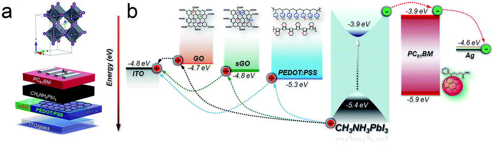 | ||
| Fig. 3 (a) Illustrative schematic of the device architecture for the inverted PHJ perovskite cell studied in this work. (b) Energy-level diagram of each layer. | ||
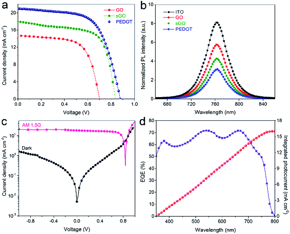 | ||
| Fig. 4 (a) J–V characteristics of the studied solar cells with different pristine HTLs. (b) PL spectra of the perovskite films on different pristine HTLs. (c) J–V curves of the best device fabricated by using sGO HTLs under AM 1.5G (100 mW cm−2) simulated solar illumination and in dark. (d) EQE spectra and the integrated photocurrent calculated under AM 1.5G solar irradiation of the glass/ITO/sGO/CH3NH3PbI3/PCBM/Ag device. | ||
Photoluminescence (PL) properties of the CH3NH3PbI3 perovskite film deposited on GO, sGO and PEDOT HTLs with ITO/glass substrate were demonstrated in Fig. 4b. Compared to the perovskite film on ITO/glass substrate, striking quenching efficiencies are showed in CH3NH3PbI3 perovskite films on GO, sGO and PEDOT HTLs, suggesting an evidence of efficient electron extraction from perovskite photoactive layer to different HTLs other than ITO/glass.48 Additionally, the J–V curves of the best performed device with the structure ITO/sGO/CH3NH3PbI3/PCBM/Ag, under illumination and in dark, is presented in Fig. 4c. This cell has achieved a maximum PCE of 9.9% with a Voc of 0.84 V, a Jsc of 17.9 mA cm−2, and a FF of 66%. The external quantum efficiency (EQE) spectra of this device is also shown in Fig. 4d, and the EQE integration over an AM 1.5G spectrum delivers a Jsc value consistent with the corresponding J–V measurement.
In order to fully explore the potential of the sGO as HTL in PSCs, we combined as-prepared sGO with commercialized PEDOT:PSS solution and obtained the sGO–PEDOT:PSS composite HTLs. Before the fabrication of the devices, optical characteristics of these composite HTLs on cleaned ITO/glass substrates were investigated, which plays an important role in photovoltaic performance of PSCs. As illustrated in Fig. 5a, the transmittance of 1:1 GO–PEDOT, 1:2 sGO–PEDOT, 1:1 sGO–PEDOT and 2:1 sGO–PEDOT HTL films show similar spectra (the inset image is the photograph of the obtained sGO–PEDOT:PSS composite HTL solutions), where high transparencies are clearly observed in the visible range from 350 nm to 800 nm. Additionally, the transmittance spectra of pristine GO, sGO and PEDOT HTLs films depicted in Fig. 5b also show similar shapes with high optical transparency and the photograph of the diluted pristine GO, sGO and PEDOT:PSS solutions is shown. These results affirm the transparency of these composite HTLs is barely affected by the incorporation of GO or sGO in the PEDOT:PSS solution.
 | ||
| Fig. 5 Transmittance spectra of (a) different composite HTLs and (b) pristine GO, sGO and PEDOT films on ITO substrates. | ||
To investigate the efficacy of the composite HTLs in PSCs, the J–V curves of these PSCs based on 1:1 GO–PEDOT, 1:2 sGO–PEDOT, 1:1 sGO–PEDOT and 2:1 GO–PEDOT HTLs with photovoltaic performance are shown in Fig. 6a. In order to make clear comparisons, the photovoltaic parameters of these devices are also shown in Table 2. Compared with the device based on pristine PEDOT:PSS HTL, the PSCs with a conventional 1:1 GO–PEDOT HTL showed a higher average PCE of 9.6 ± 0.70% with Voc of 0.86 ± 0.07 V, Jsc of 17.6 ± 1.6 mA cm−2, and FF of 64 ± 5.1%. Obviously, it is reasonable to expect the effect upon the addition of the GO, resulting in a lowering of the devices Voc and PCE. However, it is found that the PCEs of the PSCs incorporated with the sGO–PEDOT HTL are significantly higher than that from the PSCs by using the PEDOT as HTLs. When the device was using 1:2 sGO–PEDOT HTL, the Voc and Jsc increased to 0.98 ± 0.05 V and 18.9 ± 1.2 mA cm−2, respectively. Notably, in the case of the device with 1:1 sGO–PEDOT HTL, it showed a decent Voc of 1.01 ± 0.04 V, resulting in a significantly enhanced PCE of 13.0 ± 0.48%. However, further increasing the volume ratio to 2:1 (sGO:PEDOT:PSS) deteriorated the device performance with a relatively low PCE of 12.2 ± 0.45%. Meanwhile, the series resistance (Rs) and the shunt resistance (Rsh) from the PSCs based on different HTLs are also summarized in Table 2. As we know, the Rs of the solar cells is originated from the used materials, while the Rsh is aroused from the leakage current. Obviously, the Rs estimated from the PSCs based on 1:1 sGO–PEDOT HTLs is 9.4 ± 4.0 Ω cm−2, which is smaller than that (10.1 ± 4.5 and 12.3 ± 11.8 Ω cm−2) from the PSCs with 2:1 and 1:2 sGO–PEDOT HTLs, respectively. But the Rsh from the PSCs based on the 1:2, 1:1 and 2:1 sGO–PEDOT HTLs is 1482, 1588 and 1830 Ω cm−2, respectively. For solar cells, small Rs implies that there is low contact resistances, resulting on relatively higher Jsc and PCE. On the other hand, it is of great importance to keep the Rsh as high as possible since large Rsh would lead to increased FF and Voc values.49 Therefore, the PSCs based on 1:1 sGO–PEDOT HTL exhibit have the best performance with the relatively high Voc, Jsc, FF and consequently high PCE.
 | ||
| Fig. 6 (a) J–V curves of the studied solar cells with different composite HTLs. (b) PL spectra of CH3NH3PbI3 perovskite on different composite HTLs. | ||
| HTLs | Voc (V) | Jsc (mA cm−2) | FF (%) | PCEa (%) | Rs (Ω cm−2) | Rsh (Ω cm−2) |
|---|---|---|---|---|---|---|
| a Maximum values are in parentheses. | ||||||
| 1:1 GO–PEDOT |
0.86 ± 0.07 | 17.6 ± 1.6 | 64 ± 5.1 | 9.6 ± 0.70 (10.9) | 6.0 ± 1.2 | 530 ± 208 |
| 1:2 sGO–PEDOT |
0.98 ± 0.05 | 18.9 ± 1.2 | 58 ± 4.5 | 10.9 ± 0.72 (11.8) | 12.3 ± 11.8 | 1482 ± 337 |
| 2:1 sGO–PEDOT |
1.00 ± 0.05 | 19.2 ± 1.2 | 64 ± 3.7 | 12.2 ± 0.45 (12.7) | 10.1 ± 4.5 | 1830 ± 226 |
| 1:1 sGO–PEDOT |
1.01 ± 0.04 | 19.4 ± 1.1 | 67 ± 3.2 | 13.0 ± 0.48 (13.9) | 9.4 ± 4.0 | 1588 ± 365 |
In addition, in Fig. 6b, PL emission spectra of CH3NH3PbI3 perovskite films on these composite HTLs were also used to elucidate the efficacy of sGO in the composite HTLs. An obvious emission peak at around 763 nm is observed for all samples, which corresponds well to the UV-vis absorption onset (shown in ESI Fig. S2 and S3†). The PL intensity of perovskite changes very much as using different volume ratios of sGO to PEDOT:PSS in the composite HTLs. The maximum PL quench is shown when depositing CH3NH3PbI3 perovskite films on 1:1 sGO–PEDOT HTL. This means that the holes created in perovskite absorbers could travel through 1:1 sGO–PEDOT HTL more efficiently.35,50,51
To further understand the effects of different HTLs on the performance of PSCs, we used SEM to analyse the sGO, PEDOT, 1:1 GO–PEDOT and 1:1 sGO–PEDOT HTLs on ITO/glass, shown in Fig. 7. Obviously, Fig. 7a and e reveals the PEDOT HTL have a homogeneous surface with room-mean-square (RMS) surface roughness (Rq) calculated to be 2.05 nm. In contrast, pristine sGO HTL forms a continuous film, albeit with some aggregates and a relatively large Rq of 3.35 nm (Fig. 7b and f), possibly due to stacked sGO sheets. When the GO or sGO sheets were incorporated in PEDOT: PSS, the 1:1 GO–PEDOT and 1:1 sGO–PEDOT HTLs show uneven surfaces with relatively small flat cakes detected in Fig. 7c and d. It is even possible, in this case, to observe a low aggregation of the GO or sGO sheets with a good intercalation. The Rq remarkably increase to 9.21 and 13.20 nm (Fig. 7g and h), respectively, indicating the surface becomes quite rough. This is further confirmed by AFM topography images. Then, it still is worth emphasizing that these HTLs formed similar surface morphology with homogeneous distributions and additional GO/sGO sheets evenly dispersed in the PEDOT:PSS solution, corresponding to the SEM image results. In Fig. 7i–l, the surface energy or wettability of perovskite precursors on these HTLs was evaluated by contact angle measurements. The measured contact angles of perovskite precursor droplets on PEDOT, sGO, 1:1 GO–PEDOT and 1:1 sGO–PEDOT HTL substrates are 0° and 6.6°, 6.2° and 5.9°, respectively, indicating good wetting of the solvent. Although the addition of both GO and sGO into PEDOT:PSS solution increases the contact angle on ITO substrate with UV-zone treatment, these HTL films show a superior wettability and compatibility with perovskite precursor solution. These exaggerated effects are most reasonably attributed to the UV-zone treatment, which increase the surface energy with significant modification.52 The contacting angles of water on ITO-coated glass without and with 15 min of UV-zone treatment are 61° and 8° respectively, shown in ESI Fig. S4.† Importantly, the sensitivity of these HTL films on wettability can also impact on the formation of uniform perovskite films with a good coverage and electrical contact,27 which is important for fabrication of devices.
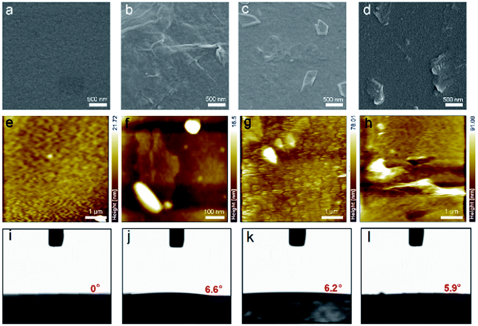 | ||
| Fig. 7 SEM images, AFM topography and perovskite precursor solution contact angels of PEDOT (a, e and i), sGO (b, f and j), 1:1 GO–PEDOT (c, g and k) and 1:1 sGO–PEDOT (d, h and l) film on ITO substrates. | ||
As observed from the SEM images in Fig. 8a–d, all the perovskite films exhibit a flat surface morphology of many crystalline grains without pin-holes. Meanwhile, the average grain sizes versus HTLs are summarized in Fig. 8i–l. The grain size of perovskite film on pristine sGO (340 nm) HTL is significantly larger than those deposited on PEDOT:PSS-based solution without (180 nm) or with the addition of GO (240 nm) or sGO (280 nm). This is because substrates providing a smooth surface with bad hydrophilic property yield a high grain boundary mobility, which enables the growth of larger grains.53 Consequently, we investigated the surface roughness and topology of the perovskite films by AFM images in Fig. 8e–h. The Rq of PEDOT, sGO, 1:1 GO–PEDOT and 1:1 sGO–PEDOT thin films were calculated to be 11.2, 13.3, 9.9 and 10.2 nm, respectively, shown in Fig. 8m, indicating the uniform perovskite films are consisted of dense and closely packed grains with size of a few hundred nanometres. Interestingly, the phenomenon we observed that the variation tendency of average grain size of these perovskite films in the presence of different HTLs is the same with that of the surface roughness. This may be explained by the fact that the larger grains can be easier to increase the surface roughness of perovskite thin films. By comparing XRD data of the perovskite films as shown in Fig. 8n, we confirmed that our presumption is quite acceptable owing to the similar features in the intensities of the peaks. Normally, these perovskites films exhibit strong characteristic diffraction patterns for CH3NH3PbI3 tetragonal crystal structure.54 In addition, there is an additive peak observed at 12.2°, which can be matched well with the (001) lattice plane of crystallized PbI2.55,56 However, a small amount of excess PbI2 having beneficial effects could be useful to enhance the performance of the devices.57
 | ||
| Fig. 8 SEM images, AFM topographies and grain size distributions of perovskite films deposited on the PEDOT (a, e and i), sGO (b, f and j), 1:1 GO–PEDOT (c, g and k) and 1:1 sGO–PEDOT (d, h and l) film substrates. Average grain size and root-mean-square surface roughness (Rq) (m) and XRD spectra (n) of perovskite films deposited on the PEDOT, sGO, 1:1 GO–PEDOT and 1:1 sGO–PEDOT film substrates. | ||
The cross-sectional SEM images of the completed devices based on PEDOT and 1:1 sGO–PEDOT HTLs are also presented in Fig. 9a and b, showing that the perovskite grains formed on 1:1 sGO–PEDOT HTLs are larger than those formed on PEDOT. Therefore, the morphology of the perovskite films based on our observations is different due to the difference in different HTL substrates, resulting in different photovoltaic performance of PSCs. For comparison, Fig. 9c–f present the statistical Voc, Jsc, FF and PCE distributions of the PSCs based on PEDOT and 1:1 sGO–PEDOT HTLs, respectively. These data are summarized from 50 devices in total. It is found that the statistical photovoltaic parameters are in accordance with Gauss distribution. As illustrated in Fig. 9c, the PSCs based on 1:1 sGO–PEDOT HTL exhibited a narrow PCE distribution with an average efficiency of 13.0%, but the PCE distribution of the PSCs based on PEDOT HTL was much broader, varying from 9.0 to 11.5% and averaging at ∼10.3%. Meanwhile, the average Jsc value for PSCs based on PEDOT and sGO–PEDOT HTLs are 17.5 ± 3.4 and 19.4 ± 1.1 mA cm−2, respectively, which indicate that the PCE improvement can be related to an increase of Jsc because of the synergetic effect of sGO and PEDOT:PSS. It is found that the average Voc values of PSCs increases from 0.88 ± 0.034 V for PEDOT HTL to 1.01 ± 0.04 V for sGO–PEDOT HTL. Therefore, these encouraging data indicate that the utilization of the 1:1 sGO–PEDOT HTL would give rise to a higher reliability and repeatability of the Voc, Jsc and PCE enhancements. In particular, it is worth pointing out that the reproducibility of the PSCs based on sGO–PEDOT HTL is higher than that of the PSCs based on the pristine PEDOT HTL.
 | ||
| Fig. 9 The cross-sectional SEM of devices with PEDOT (a) and 1:1 sGO–PEDOT (b) as HTLs. Histograms of photovoltaic parameters for the solar cells with PEDOT and 1:1 sGO–PEDOT as HTLs: (c) Voc, (d) Jsc, (e) FF and (f) PCE. | ||
It has been reported that the hysteresis behavior typically appeared in J–V curves of planar perovskite solar cells, which are related to both the grain size of perovskite films and charge recombination or barriers at the perovskite/HTL interfaces.49,58 Fig. 10a and b show the J–V curves of PSCs based on PEDOT and sGO–PEDOT HTLs measured under different scan directions. The detailed photovoltaic parameters of PSCs measured under different scan directions are summarized in Table 3. The PSCs using PEDOT HTL achieved a PCE of 11.5% (9.5%) when measured under the reverse (forward) scan, showing a large degree of hysteresis (a 17.4% deviation). While for the PSCs based on sGO–PEDOT HTL, the PCE is 13.9% at the reverse scan, and the PCE is 13.0% at the forward scan, indicating a 6.5% deviation between different scan directions. It is seen that both the PSCs exhibit J–V hysteresis phenomenon under different scan directions and the larger PCE is obtained when the reverse scan is applied. It is clear that the use of sGO–PEDOT composite HTL helps to improve the device performance and reduce the degree of hysteresis as compared with the pristine PEDOT HTL. Meanwhile, the measured external quantum efficiency (EQE) spectra of the representative devices using PEDOT and sGO–PEDOT HTLs are displayed in Fig. 10c, suggesting the photo-to-electron conversion of the fabricated device. It is clearly seen that the device based on sGO–PEDOT HTL possess higher photo-to-electron conversion compared with the pristine PEDOT based device. It is understandable that the integrated currents from the EQE curves are in general lower than the corresponding Jsc values obtained from the J–V measurements.
 | ||
| Fig. 10 J–V characteristics of perovskite solar cells fabricated by using PEDOT (a) and 1:1 sGO–PEDOT (b) HTLs and measured at: forward scan (from 0 V to 1.1 V) and reverse scan (from 1.1 V to 0 V) at the scan rate 1.25 V s−1. (c) External quantum efficiency (EQE) spectra of perovskite solar cells fabricated by using PEDOT and sGO–PEDOT as HTLs. (d) Time-resolved photoluminescence measurements of perovskite films on PEDOT and sGO–PEDOT HTLs, the lines are obtained by fitting the data using a bi-exponential rate law. | ||
| PSCs with different HTLs | Scan direction | Voc (V) | Jsc (mA cm−2) | FF (%) | PCE (%) |
|---|---|---|---|---|---|
| PEDOT | Forward | 0.82 | 20.9 | 55 | 9.5 |
| Reverse | 0.88 | 20.9 | 63 | 11.5 | |
| 1:1 sGO–PEDOT |
Forward | 0.94 | 20.8 | 67 | 13.0 |
| Reverse | 0.95 | 20.4 | 72 | 13.9 |
To understand why the device with sGO–PEDOT as HTL exhibits better photovoltaic performance and less photocurrent hysteresis than that of the PSCs-based on PEDOT HTL, the time-resolve photoluminescence spectra (TRPL) spectra of perovskite films with PEDOT and sGO–PEDOT HTLs are conducted in Fig. 10d. Because the TRPL spectra can get insight into perovskite photophysical properties, including the charge accumulation at perovskite/HTL interface with charge transfer or charge separation/injection behaviour.59 The TRPL spectra were fitted by a bi-exponential function: PLintensity = A1exp(−t/τ1) + A2exp(−t/τ2); where A1 and A2 are time independent coefficients of amplitude fraction for each decay component and τ1 and τ2 are decay time of fast and slow component, respectively. The fitted parameters are depicted in Table 4. It can be observed clearly that the decay time decreases from 16.9 to 4.3 ns, which suggests the charge carriers generated in perovskite are more efficiently transferred in the sGO–PEDOT HTL than PEDOT HTL. It is noted that a fast charge transfer and collection process occurs in the perovskite/sGO–PEDOT interface.59 This means that this improvement in photo-induced carrier transfer and injection process might avoid the formation of perovskite/HTL interface capacitance or accumulated charge,60 which ultimately result in good device performance and reduced J–V hysteresis.
| HTLs | A1 | τ1 (ns) | A2 | τ2 (ns) | τ (ns) |
|---|---|---|---|---|---|
| PEDOT | 22.908 | 0.802 | 77.092 | 25.044 | 16.9 |
| 1:1 sGO–PEDOT |
66.308 | 0.436 | 33.692 | 17.861 | 4.3 |
4. Conclusions
In summary, we identified an efficient method to prepare sulfated graphene oxide (sGO). FTIR, Raman, TGA and XPS measurements showed that the solution-processable sGO was successfully synthesized. Here, the sGO, as a new HTL was used to replace the conventional used GO and PEDOT:PSS in inverted planar PSCs. The PSCs based on sGO HTL exhibit better device characteristics than those of the reference device using GO HTL. More importantly, we have prepared the sGO–PEDOT composite HTL for use as a HTL in PSCs by combining solution-processable sGO with commercialized PEDOT:PSS solution. By applying such an efficient HTL, the PCE of the device achieved with high reproducibility was improved by 21% compared to that with pristine PEDOT:PSS HTL. Therefore, this promising strategy provides an efficient and simple way to approach the ideal HTM for the advancement of practical PSCs.Conflicts of interest
There are no conflicts to declare.Acknowledgements
We acknowledge the financial support from the Recruitment Program of Global Young Experts of China and Sichuan one thousand Talents Plan.Notes and references
- D. Bi, C. Yi, J. Luo, J. D. Décoppet, F. Zhang, S. M. Zakeeruddin, X. Li, A. Hagfeldt and M. Grätzel, Nat. Energy, 2016, 1, 16142 CrossRef CAS.
- Y. C. Hsiao, T. Wu, M. Li and B. Hu, Adv. Mater., 2015, 27, 2899–2906 CrossRef CAS PubMed.
- M. Z. Liu, M. B. Johnston and H. J. Snaith, Nature, 2013, 501, 395–398 CrossRef CAS PubMed.
- J. H. Im, C. R. Lee, J. W. Lee, S. W. Park and N. G. Park, Nanoscale, 2011, 3, 4088–4093 RSC.
- A. Kojima, K. Teshima, Y. Shirai and T. Miyasaka, J. Am. Chem. Soc., 2009, 131, 6050–6051 CrossRef CAS PubMed.
- Y. Bai, Q. Dong, Y. Shao, Y. Deng, Q. Wang, L. Shen, D. Wang, W. Wei and J. S. Huang, Nat. Commun., 2016, 7, 12806 CrossRef CAS PubMed.
- W. Ke, G. Fang, J. Wan, H. Tao, Q. Liu, L. Xiong, P. Qin, J. Wang, H. Lei, G. Yang, M. Qin, X. Zhao and Y. Yan, Nat. Commun., 2015, 6, 6700 CrossRef CAS PubMed.
- H. P. Zhou, Q. Chen, G. Li, S. Luo, T. B. Song, H. S. Duan, Z. R. Hong, J. B. You, Y. S. Liu and Y. Yang, Science, 2014, 345, 542–546 CrossRef CAS PubMed.
- T. Leijtens, G. E. Eperon, S. Pathak, A. Abate, M. M. Lee and H. J. Snaith, Nat. Commun., 2013, 4, 2885 Search PubMed.
- X. Song, W. Wang, P. Sun, W. Ma and Z. K. Chen, Appl. Phys. Lett., 2015, 106, 033901 CrossRef.
- H. Kim, K. G. Lim and T. W. Lee, Energy Environ. Sci., 2016, 9, 12–30 CAS.
- M. Saliba, S. Orlandi, T. Matsui, S. Aghazada, M. Cavazzini, J. P. Correa-Baena, P. Gao, R. Scopelliti, E. Mosconi, K. H. Dahmen, F. De Angelis, A. Abate, A. Hagfeldt, G. Pozzi, M. Graetzel and M. K. Nazeeruddin, Nat. Energy, 2016, 1, 15017 CrossRef CAS.
- J. B. You, Z. R. Hong, Y. Yang, Q. Chen, M. Cai, T. B. Song, C. C. Chen, S. R. Lu, Y. S. Liu, H. P. Zhou and Y. Yang, ACS Nano, 2014, 8, 1674–1680 CrossRef CAS PubMed.
- F. Zhang, C. Yi, P. Wei, X. Bi, J. Luo, G. Jacopin, S. Wang, X. Li, Y. Xiao, S. M. Zakeeruddin and M. Grätzel, Adv. Energy Mater., 2016, 6, 1600401 CrossRef.
- J. Y. Jeng, K. C. Chen, T. Y. Chiang, P. Y. Lin, T. D. Tsai, Y. C. Chang, T. F. Guo, P. Chen, T. C. Wen and Y. J. Hsu, Adv. Mater., 2014, 26, 4107–4113 CrossRef CAS PubMed.
- K. Domanski, J. P. Correa-Baena, N. Mine, M. K. Nazeeruddin, A. Abate, M. Saliba, W. Tress, A. Hagfeldt and M. Gratzel, ACS Nano, 2016, 10, 6306–6314 CrossRef CAS PubMed.
- Z. Xiao, C. Bi, Y. Shao, Q. Dong, Q. Wang, Y. Yuan, C. Wang, Y. Gao and J. S. Huang, Energy Environ. Sci., 2014, 7, 2619 CAS.
- F. Zhang, J. Song, L. Zhang, F. Niu, Y. Hao, P. Zeng, H. Niu, J. Huang and J. Lian, J. Mater. Chem. A, 2016, 4, 8554–8561 CAS.
- Y. Bai, Y. Fang, Y. Deng, Q. Wang, J. Zhao, X. Zheng, Y. Zhang and J. Huang, ChemSusChem, 2016, 9, 2686–2691 CrossRef CAS PubMed.
- W. Yu, X. Xie, Y. Li, Y. Li, R. Chen, X. Qiu and W. Huang, J. Mater. Chem. C, 2016, 4, 8077–8085 RSC.
- B. H. Fan, X. G. Mei and J. Y. Ouyang, Macromolecules, 2008, 41, 5971–59738 CrossRef CAS.
- W. Y. Chen, L. L. Deng, S. M. Dai, X. Wang, C. B. Tian, X. X. Zhan, S. Y. Xie, R. B. Huang and L. S. Zheng, Adv. Funct. Mater., 2005, 15, 203–208 CrossRef.
- J. P. Thomas and K. T. Leung, J. Mater. Chem. A, 2016, 4, 17537–17542 CAS.
- J. P. Thomas, L. Zhao, D. McGillivray and K. T. Leung, J. Mater. Chem. A, 2014, 2, 2383 CAS.
- W. Y. Chen, L. L. Deng, S. M. Dai, X. Wang, C. B. Tian, X. X. Zhan, S. Y. Xie, R. B. Huang and L. S. Zheng, J. Mater. Chem. A, 2015, 3, 19353–19359 CAS.
- J. Zhang, C. Shi, J. Chen, C. Ying, N. Wu and M. Wang, J. Semicond., 2016, 37, 033002 CrossRef.
- A. Giuri, S. Masi, S. Colella, A. Kovtun, S. Dell'Elce, E. Treossi, A. Liscio, C. Esposito Corcione, A. Rizzo and A. Listorti, Adv. Funct. Mater., 2016, 26, 6985–6994 CrossRef CAS.
- D. H. Wang, J. K. Kim, J. H. Seo, I. Park, B. H. Hong, J. H. Park and A. J. Heeger, Angew. Chem., Int. Ed. Engl., 2013, 52, 2874–2880 CrossRef CAS PubMed.
- S. Lee, S. Lim, E. Lim and K. L. Lee, J. Phys. Chem. Solids, 2010, 71, 483–486 CrossRef CAS.
- J. Liu, Y. Xue, M. Zhang and L. Dai, MRS Bull., 2012, 37, 1265–1272 CrossRef CAS.
- N. Arora, M. I. Dar, A. Hinderhofer, N. Pellet, F. Schreiber, S. M. Zakeeruddin and M. Grätzel, Science, 2017 DOI:10.1126/science.aam5655.
- D. Y. Lee, S. I. Na and S. S. Kim, Nanoscale, 2016, 8, 1513–1522 RSC.
- S. S. Li, K. H. Tu, C. C. Lin, C. W. Chen and M. Chhowalla, ACS Nano, 2014, 4, 3169–3174 CrossRef PubMed.
- J. Liu, Y. Xue, Y. Gao, D. Yu, M. Durstock and L. Dai, Adv. Mater., 2012, 24, 2228–2233 CrossRef CAS PubMed.
- J. S. Yeo, R. Kang, S. Lee, Y. J. Jeon, N. Myoung, C. L. Lee, D. Y. Kim, J. M. Yun, Y. H. Seo, S. S. Kim and S. I. Na, Nano Energy, 2015, 12, 96–104 CrossRef CAS.
- Q. Luo, Y. Zhang, C. Liu, J. Li, N. Wang and H. Lin, J. Mater. Chem. A, 2015, 3, 15996–16004 CAS.
- A. L. Palma, L. Cinà, S. Pescetelli, A. Agresti, M. Raggio, R. Paolesse, F. Bonaccorso and A. Di Carlo, Nano Energy, 2016, 22, 349–360 CrossRef CAS.
- L. M. Dai, Acc. Chem. Res., 2013, 46, 31–42 CrossRef CAS PubMed.
- P. D. McCrary, P. A. Beasley, S. A. Alaniz, C. S. Griggs, R. M. Frazier and R. D. Rogers, Angew. Chem., Int. Ed. Engl., 2012, 51, 9784–9787 CrossRef CAS PubMed.
- J. Liu, Y. Xue and L. Dai, J. Phys. Chem. Lett., 2012, 3, 1928–1933 CrossRef CAS PubMed.
- D. Shi, V. Adinolfi, R. Comin, M. J. Yuan, E. Alarousu, A. Buin, Y. Chen, S. Hoogland, A. Rothenberger, K. Katsiev, Y. Losovyj, X. Zhang, P. A. Dowben, O. F. Mohammed, E. H. Sargent and O. M. Bakr, Science, 2015, 347, 519–521 CrossRef CAS PubMed.
- M. Ghiaci and M. Ghazaie, Catal. Commun., 2016, 87, 70–73 CrossRef CAS.
- S. Pei and H. M. Cheng, Carbon, 2012, 50, 3210–3228 CrossRef CAS.
- D. Konios, M. M. Stylianakis, E. Stratakis and E. Kymakis, J. Colloid Interface Sci., 2014, 430, 108–112 CrossRef CAS PubMed.
- Y. H. Huang, J. H. Chen, X. Sun, Z. B. Su, H. T. Xing, S. R. Hu, W. Weng, H. X. Guo, W. B. Wu and Y. S. He, Sens. Actuators, B, 2015, 212, 165–173 CrossRef CAS.
- Y. Y. Yang, Z. H. Ni, T. Yu, Z. X. Shen, H. M. Wang, Y. H. Wu, W. Chen and A. T. S. Wee, J. Phys. Chem. C, 2008, 112, 10637–10640 Search PubMed.
- S. Thakur and N. Karak, Carbon, 2012, 50, 5331–5339 CrossRef CAS.
- J. You, L. Meng, T. B. Song, T. F. Guo, Y. M. Yang, W. H. Chang, Z. Hong, H. Chen, H. Zhou, Q. Chen, Y. Liu, N. De Marco and Y. Yang, Nat. Nanotechnol., 2016, 11, 75–81 CrossRef CAS PubMed.
- X. Huang, K. Wang, C. Yi, T. Meng and X. Gong, Adv. Energy Mater., 2016, 6, 1501773 CrossRef.
- B. Cai, Y. Xing, Z. Yang, W. H. Zhang and J. Qiu, Energy Environ. Sci., 2013, 6, 1480 CAS.
- H. Chen, Z. Wei, H. He, X. Zheng, K. S. Wong and S. Yang, Adv. Energy Mater., 2016, 6, 1502087 CrossRef.
- A. Garcia, G. C. Welch, E. L. Ratcliff, D. S. Ginley, G. C. Bazan and D. C. Olson, Adv. Mater., 2012, 24, 5368–5373 CrossRef CAS PubMed.
- C. Bi, Q. Wang, Y. Shao, Y. Yuan, Z. Xiao and J. S. Huang, Nat. Commun., 2015, 6, 7747 CrossRef CAS PubMed.
- Y. Liu, Z. Yang, D. Cui, X. Ren, J. Sun, X. Liu, J. Zhang, Q. Wei, H. Fan, F. Yu, X. Zhang, C. Zhao and S. F. Liu, Adv. Mater., 2015, 27, 5176–5183 CrossRef CAS PubMed.
- L. Zhao, D. Luo, J. Wu, Q. Hu, W. Zhang, K. Chen, T. Liu, Y. Liu, Y. Zhang, F. Liu, T. P. Russell, H. J. Snaith, R. Zhu and Q. Gong, Adv. Funct. Mater., 2016, 26, 3508–3514 CrossRef CAS.
- T. J. Jacobsson, J. P. Correa-Baena, E. Halvani Anaraki, B. Philippe, S. D. Stranks, M. E. Bouduban, W. Tress, K. Schenk, J. Teuscher, J. E. Moser, H. Rensmo and A. Hagfeldt, J. Am. Chem. Soc., 2016, 138, 10331–10343 CrossRef CAS PubMed.
- D. Y. Son, J. W. Lee, Y. J. Choi, I. H. Jang, S. Lee, P. J. Yoo, H. Shin, N. Ahn, M. Choi, D. Kim and N. G. Park, Nat. Energy, 2016, 1, 16081 CrossRef CAS.
- W. Ke, C. Xiao, C. Wang, B. Saparov, H. S. Duan, D. Zhao, Z. Xiao, P. Schulz, S. P. Harvey, W. Liao, W. Meng, Y. Yu, A. J. Cimaroli, C. S. Jiang, K. Zhu, M. Al-Jassim, G. Fang, D. B. Mitzi and Y. Yan, Adv. Mater., 2016, 28, 5214–5221 CrossRef CAS PubMed.
- M. Li, X. Yan, Z. Kang, X. Liao, Y. Li, X. Zheng, P. Lin, J. Meng and Y. Zhang, ACS Appl. Mater. Interfaces, 2017, 9, 7224–7231 CAS.
- J. H. Heo, M. S. You, M. H. Chang, W. Yin, T. K. Ahn, S. J. Lee, S. J. Sung, D. H. Kim and S. H. Im, Nano Energy, 2015, 15, 530–539 CrossRef CAS.
Footnote |
| † Electronic supplementary information (ESI) available. See DOI: 10.1039/c7ra10113a |
| This journal is © The Royal Society of Chemistry 2017 |