DOI:
10.1039/C7RA10018C
(Paper)
RSC Adv., 2017,
7, 47125-47131
Composition analysis of two different PEDOT:PSS commercial products used as an interface layer in Au/n-Si Schottky diode†
Received
8th September 2017
, Accepted 2nd October 2017
First published on 6th October 2017
Abstract
The water based highly conductive transparent poly(3,4-ethylenedioxythiophene):poly(4-styrenesulfonate) (PEDOT:PSS) polymer is a promising material for many optoelectronic device applications. Chemical composition of PEDOT:PSS plays a key role to improve the performance of the devices. Two different PEDOT:PSS commercial products (PH1000 and HTL Solar) have been used as an interface layer in Au/PEDOT:PSS/n-Si Schottky barrier diodes (SBDs). The effective barrier height increased and the ideality factor decreased with the increase of temperature. Such behavior is attributed to the inhomogeneity and formation of interface dipole affecting electron injection at the interface. The Richardson constant value was obtained from ln(I0/T2) vs. 1000/T plot which is very low from the known theoretical value but the modified Richardson plot ln(I0/T2) − (qσ0)2/2(kT)2 vs. 1000/T gives the closer theoretical value of n-type silicon. The Schottky parameters were extracted from temperature dependent I–V characteristics and successfully explained by thermionic emission (TE) theory. The superiority of HTL Solar product in Au/PEDOT:PSS/n-Si SBDs could be associated for stronger inversion or better passivation on silicon surface compared to PH1000.
1. Introduction
Poly(3,4-ethylenedioxythiophene):poly(styrenesulfonate) is a water-based, high work function and p-type polymer. It is a suitable material for many semiconductor device application1,2 due to its excellent optoelectronic properties such as high conductivity,3 high transparency,4 thermal stability5 and can be easily deposit by any solution process6,7 at room temperature. The fascinating properties of PEDOT:PSS have led scientists to have tremendous motivation to explore the possibilities of using these properties for technological applications. Nowadays, the application of PEDOT:PSS thin films are not limited only to organic devices but also extend to organic/inorganic hybrid semiconductor devices.8,9,10 Metal-polymer-semiconductor (MPS) Schottky diodes are the simplest devices to fully understand the nature of the electrical behavior of the polymer. Lin et.al.11 proposed that a higher quality Schottky junctions are formed on n-Si using spin-coating PEDOT:PSS as the metal electrode. Here spin coated PEDOT:PSS (PH1000 and HTL Solar) polymer thin films are used as an interface layer between gold and n-type Si. However several research groups are working on different conducting polymers as an interface layer to improve their device performance.12,13,14 Attempts have so far to enhance the rectification properties of Au/PEDOT:PSS/n-Si Schottky device by induce a stronger inversion layer or to nicely passivate the silicon surface is a recent challenge to the researcher. Therefore changing the chemical composition, morphology and conductivity of PEDOT:PSS thin film will possible to improve the performance the devices.
In this present work, the comparative compositional and structural study on both PEDOT:PSS (PH1000 and HTL Solar) thin films and then it's used as an interface layer between gold and n-type silicon. Chemical composition and surface structure of spin coated PEDOT:PSS thin films were characterized by XPS, SEM and AFM techniques. Fabricated Au/PEDOT:PSS/n-Si SBDs were characterized by I–V measurement under reverse and forward bias conditions to understand the current conduction mechanism as well as their performance under the temperature ranging from 290 K to 380 K. Different electrical parameters namely ideality factor (n), barrier height (ϕb0), series resistance (Rs), activation energy (Ea) and Richardson constant (A*) are calculated and discuss.
2. Experimental
2.1 Device fabrications
Double side polished n-type float zone c-Si (100) wafers were used as a substrate. Resistivity and thickness of the wafers were 2.5 Ω cm and 280 μm respectively. The wafers were cleaned by standard RCA cleaning and dipped in 1% HF acid during 1 minute for native oxide removal. Two different PEDOT:PSS, HTL Solar and PH1000 solutions (Heraeus Clevios, USA) were deposited by spin coating technique with a spanning rate 1000 rpm for 60 seconds. After that the films were annealed at 130 °C for 30 minutes in nitrogen atmosphere. To make a Schottky contact a high purity gold was deposited by thermal evaporation process through a shadow mask. At the end more than 1 μm thick aluminum was thermally evaporated as a back ohmic contact.
2.2 Characterizations
Chemical composition of deposited PEDOT:PSS thin films were characterized by X-ray photospectrometry (XPS) scans (SPECS system, Phoibos 150 detector, Germany) at 3 × 10⁻⁹ mbar from a PEDOT:PSS/n-Si substrate using a nonmonochromatic Al-Kα source (1486.6 eV). The microstructure image of PEDOT:PSS thin films were studied using a scanning electron microscope (FESEM, Model: JEOL JSM-5800 Scanning Microscope). Atomic Force Microscopy (AFM) images were obtained in non contact mode using a MultiMode Nanoscope (Agilent, 5500 Atomic Force Microscope, USA). Ultrasharp tips (Noncontact “Golden” Silicon cantilevers, NSG10S) were used. The current–voltage (I–V) measurements were performed by a Keithley 2400 source meter at a temperature range between 290 K and 380 K using temperature controller.
3. Results and discussion
3.1 Structural characterizations
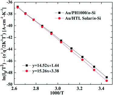
3.1.1 XPS. X-ray photospectrometry is determined the surface chemical composition and their oxidation states of PEDOT:PSS films deposited using the same spin coating conditions on silicon substrate. Fig. 1(a) shows the general scan of XPS of high-resolution core level spectra of fluorine, carbon, oxygen and sulfur in both PH1000 and HTL Solar. High-resolution peak areas and intensities of O 1s, C 1s and S 2p core level spectra are presented in Fig. 1(b–d). Almost identical spectra are obtained for the PH1000 and HTL Solar PEDOT:PSS films. However observed changes in relative signal are analyzed to deduce the elements which are involved to use for analysis. For C 1s spectra of both PEDOT:PSS films are the strongest peak at 284.8 eV originates C–C bonds. Other two peaks are at 286.2 eV and 287.7 eV related to C–O–C and C–S bonds respectively.15 In comparing to C 1s spectra, obtained for PH1000 have reduced its intensity as well as C–S bond is shifted to 0.5 eV than that of HTL Solar. The O 1s peaks of PH1000 and HTL Solar, the spectra reveal three major peaks at 531.8 eV, 533.2 eV and 535.3 eV corresponding to S![[double bond, length as m-dash]](https://www.rsc.org/images/entities/char_e001.gif) O, O–H, and C–O–C bonds respectively16 assigned to functional groups on the PEDOT and PSS chains are exactly in the same position. But the intensity of all three peaks of HTL Solar is significantly higher than PH1000 product. For this reason the charge distribution through SO, O–H and C–O–C bonds of PEDOT are better for HTL Solar which is responsible to enhance the electrical property that observed from I–V measurement. On the other hand O–H bonds could help to passivate silicon interface by acting as a diffusion barrier to minimize the surface oxidation which reduced the leakage current and increase rectification behavior. The deconvolution of S 2p peak at 168.2 eV and 164.2 eV are assigned to the sulfur signal from the PSS and PEDOT chains. Each peak from a spin-split doublet are distinguishable, centred at 164.2 eV and 168.5 eV, each with a spin–orbit splitting of 1.2 eV and a peak area ratio (2p3/2/2p1/2) of 2
O, O–H, and C–O–C bonds respectively16 assigned to functional groups on the PEDOT and PSS chains are exactly in the same position. But the intensity of all three peaks of HTL Solar is significantly higher than PH1000 product. For this reason the charge distribution through SO, O–H and C–O–C bonds of PEDOT are better for HTL Solar which is responsible to enhance the electrical property that observed from I–V measurement. On the other hand O–H bonds could help to passivate silicon interface by acting as a diffusion barrier to minimize the surface oxidation which reduced the leakage current and increase rectification behavior. The deconvolution of S 2p peak at 168.2 eV and 164.2 eV are assigned to the sulfur signal from the PSS and PEDOT chains. Each peak from a spin-split doublet are distinguishable, centred at 164.2 eV and 168.5 eV, each with a spin–orbit splitting of 1.2 eV and a peak area ratio (2p3/2/2p1/2) of 2![[thin space (1/6-em)]](https://www.rsc.org/images/entities/char_2009.gif) :1. From the integrated peak areas of each component of PSS and PEDOT are calculated. The ratio of PSS/PEDOT of PH1000 and HTL Soar is 1.9 and 2.4 respectively. Since an excess of PSS in HTL Solar product leads to increase the work function of PEDOT:PSS.17 As a consequence there is a substantial shift in work function of PEDOT:PSS and in electron affinity of silicon. The shift of Δ is consider to the band bending (BB) and formed a dipole at the interface between PEDOT:PSS and n-Si.11,18 Due to large shift of Δ is responsible to increase the band banding of PEDOT:PSS(HTL Solar)/n-Si junction. Therefore large number of charge carriers are accumulated at the interface and formed a stronger dipole compare to PEDOT:PSS(PH1000)/n-Si junction. Thus the rectification property of HTL Solar is better than that of PH1000 discuss later. Subsequently contact angle of HTL Solar is less due to the excess of PSS content.19 Therefore HTL Solar product could be uniformly deposit on hydrophobic silicon surface in a large area without using any surfactant.
:1. From the integrated peak areas of each component of PSS and PEDOT are calculated. The ratio of PSS/PEDOT of PH1000 and HTL Soar is 1.9 and 2.4 respectively. Since an excess of PSS in HTL Solar product leads to increase the work function of PEDOT:PSS.17 As a consequence there is a substantial shift in work function of PEDOT:PSS and in electron affinity of silicon. The shift of Δ is consider to the band bending (BB) and formed a dipole at the interface between PEDOT:PSS and n-Si.11,18 Due to large shift of Δ is responsible to increase the band banding of PEDOT:PSS(HTL Solar)/n-Si junction. Therefore large number of charge carriers are accumulated at the interface and formed a stronger dipole compare to PEDOT:PSS(PH1000)/n-Si junction. Thus the rectification property of HTL Solar is better than that of PH1000 discuss later. Subsequently contact angle of HTL Solar is less due to the excess of PSS content.19 Therefore HTL Solar product could be uniformly deposit on hydrophobic silicon surface in a large area without using any surfactant.
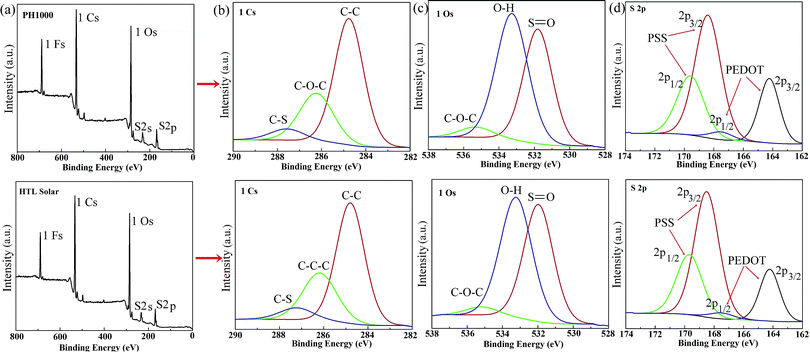 |
| | Fig. 1 Chemical composition analysis of the PEDOT:PSS(PH1000 and HTL Solar) thin film using X-ray photospectrometry: (a) general scan of XPS of high-resolution core level spectra, (b–d) deconvolution of C 1s, O 1s and S 2p core level of PH1000 and HTL Solar PEDOT:PSS thin films. | |
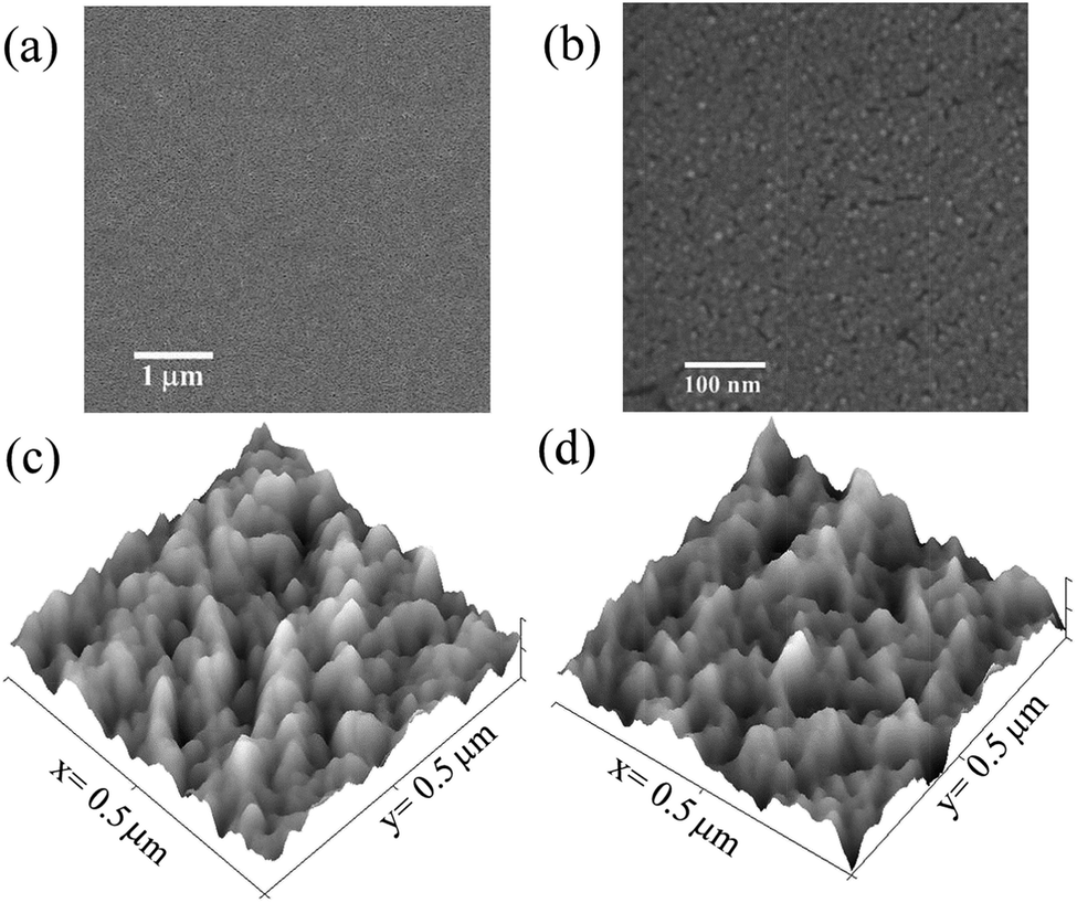
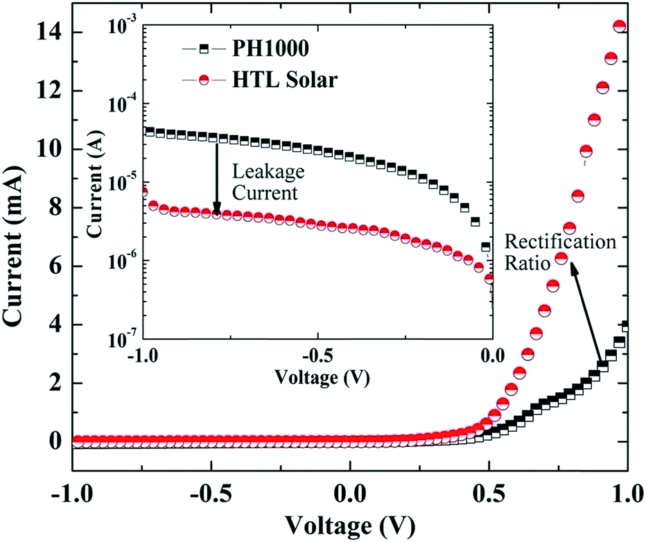
3.1.2 SEM and AFM. Surface morphology of both PEDOT:PSS thin films are shown in Fig. 2(a and b). From the morphology, it is clear that the films are smooth, continuous and uniform without cracks and holes on a large scale. The films are composed of PEDOT:PSS nanoparticles are closely packed with each other to form a chain matrix. AFM measurement was used to observe surface topology at high-resolution the three-dimensional view of PEDOT:PSS thin layers of PH1000 and HTL Solar shown in Fig. 2(c and d). The AFM image suggest that the PEDOT:PSS nanoparticles are associated with each other and thoroughly distributed all over the film surface. The estimated surface roughness of PEDOT:PSS films are found to vary within the range from 2 to 3 nm.
 |
| | Fig. 2 Structural characteristics of the PEDOT:PSS thin films: (a) scanning electron micrographs of PEDOT:PSS (HTL Solar) thin film on a large scale and (b) PEDOT:PSS (PH1000) thin film on a small scale, three-dimensional atomic force microscopy view of both PEDOT:PSS layers (c) PH1000 and (d) HTL Solar. | |
3.2 Electrical characterization
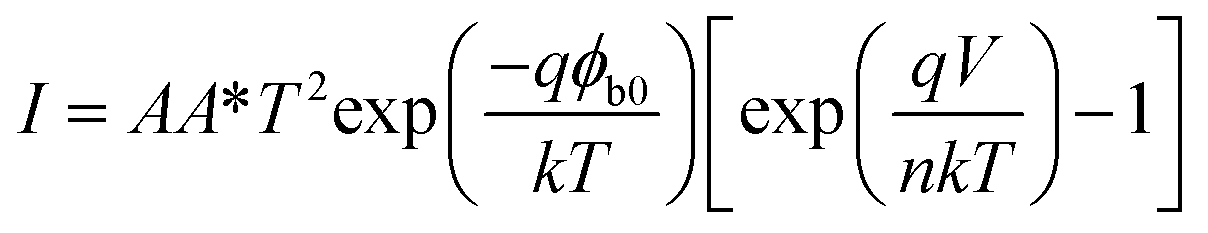
Fig. 3 shows the room temperature (290 K) current–voltage characteristic of Au/PEDOT:PSS/n-Si Schottky barrier diodes (SBDs) for both PEDOT:PSS compound. They are showed a rectifying behavior of the Schottky diodes. The rectification ratio at 1 V of HTL Solar product has increased 5 times more compared to PH1000 product. Better rectification property suggests that the surface property of interface layer plays an important role to determine the ideality factor and actual barrier height of the Schottky junction. The charge transportation through the interface layer caused by well passivated and strong interface dipole in uniform and sub-atomic structure of HTL Solar product could be responsible for the transition of the low leakage current compared to PH1000. The leakage current of Au/HTL Solar/n-Si SBDs is 10 times less than that of Au/PH1000/n-Si SBDs shown in the inset of Fig. 3.
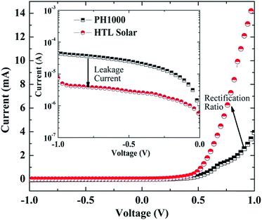 |
| | Fig. 3 Room temperature (290 K) current–voltage characteristics of Au/P1000/n-Si and Au/HTL Solar/n-Si SBDs. | |
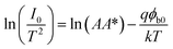
Current–voltage characteristics of SBDs at forward and reverse bias (neglecting series and shunt resistance) is expressed by20,21
| |
 | (1) |
where
A is the area of diode (
A = 0.1256 cm
2),
ϕb0 is the barrier height,
q is the electron charge,
k is the Boltzmann constant.
T is the absolute temperature,

is Richardson's constant and the value is 120 A cm
−2 K
−2 for n-type Si.
22 The ideality factor and barrier height of the Schottky barrier diodes are describe the deviation of the experimental temperature dependent
I–
V data is expressed as:
23,24| |
 | (2) |
| |
 | (3) |
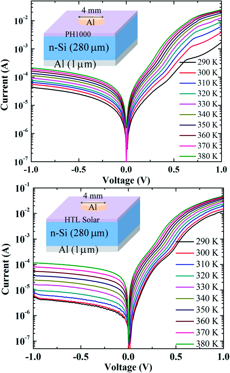
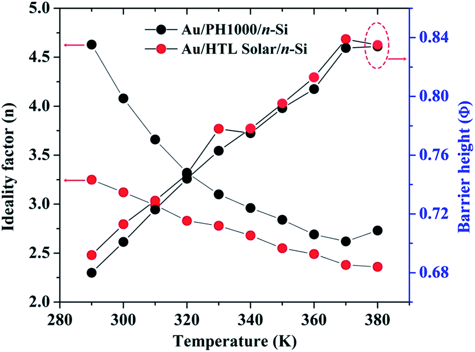
Fig. 4 shows the semi-logarithmic forward and reverse bias I–V characteristics of the Au/PH1000/n-Si and Au/HTL Solar/n-Si SBDs in the temperature ranging from 290 K to 380 K. From intercept and slope of lnI vs. V plot at each temperature gives the ϕb0 and n respectively. The experimental value of n and ϕb0 are obtained from depending on temperature. The range of ϕb0 and n for Au/PH1000/n-Si SBDs are from 0.680 eV and 4.63 at 290 K to 0.835 eV and 2.73 at 380 K. In addition for Au/HTL Solar/n-Si SBDs are from 0.692 eV and 3.25 at 290 K to 0.834 eV and 2.36 at 380 K respectively. Calculated ϕb0 value increase and n decrease with the increasing temperature (shown in Fig. 5) due to an inhomogeneity occurs in between MS interface which becomes more pronounced with the increases of temperature. This suggests that the use of PEDOT:PSS as an interface layer modifies the effective barrier height as well as its occurs inhomogeneity at the interface between gold and silicon. It is observed that the barrier height of Au/HTL Solar/n-Si SBDs is slightly higher and ideality factor is lower than that of Au/PH1000/n-Si Schottky diodes at room temperature measurement. This could be attributed to better rectification property of HTL Solar product than that of PH1000. The presence of HTL Solar layer on Au/n-Si Schottky contact exhibited to decrease the ideality factor as compare to PH1000. The calculated barrier height and ideality factor at each temperature of Au/PH1000/n-Si and Au/HTL Solar/n-Si SBDs are shown in Table 1 in the ESI.†
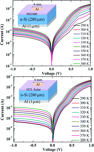 |
| | Fig. 4 Forward and reversed bias current–voltage (I–V) characteristics of Au/PEDOT:PSS/n-Si SBDs in the temperature range 290–380 K. | |
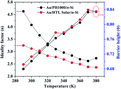 |
| | Fig. 5 Temperature dependence of ideality factor (n) and barrier height (ϕ) of Au/PEDOT:PSS/n-Si SBDs. | |
Table 1 Activation energy and Richardson constant calculated from Richardson and modified Richardson plot
| SBDs |
Richardson plot |
Modified Richardson plot |
| Ea (eV) |
A* (A cm−2 K−2) |

(eV) |
σs |
Ea (eV) |
A* (A cm−2 K−2) |
| Au/PH1000/n-Si |
0.20 |
3.75 × 10⁻⁷ |
1.30 |
0.181 |
1.25 |
33.60 |
| Au/HTL Solar/n-Si |
0.24 |
1.93 × 10⁻⁶ |
1.38 |
0.174 |
1.31 |
233.84 |
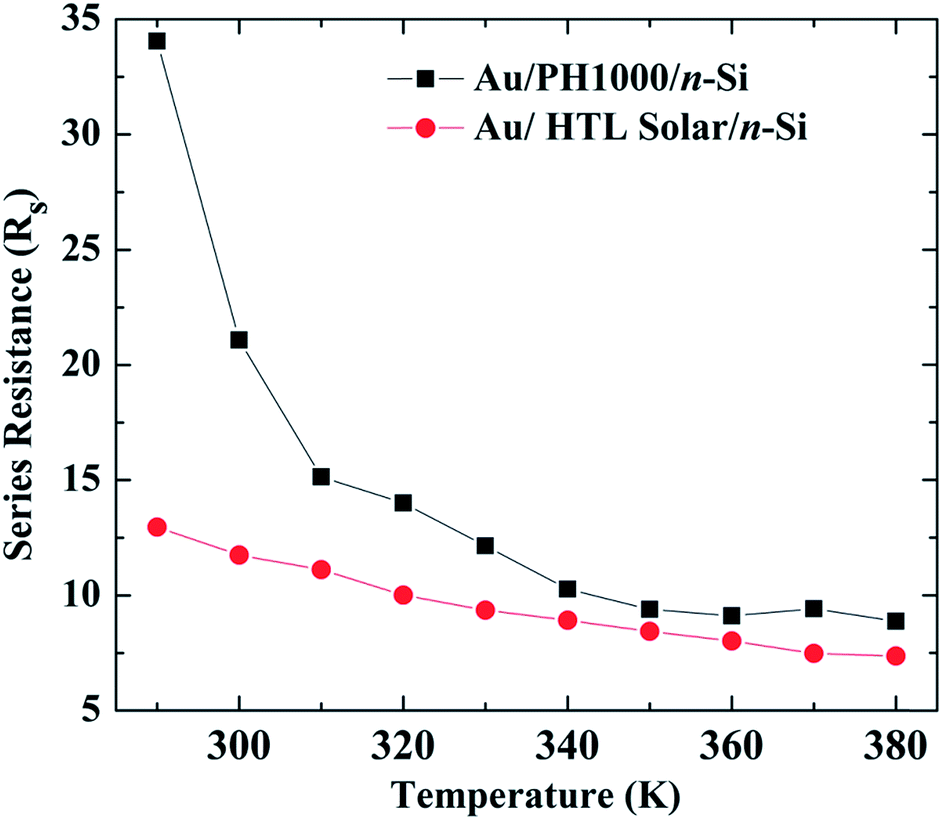
Cheung model25 is used to accurately determine the Schottky parameters such as ideality factor and barrier height of Au/PEDOT:PSS/n-Si SBDs and simultaneously evaluate the series resistance (Rs) of the SBDs. Calculated values of n, ϕb0 and Rs are shown Table 1 in the ESI.† It is observed that the series resistance of Au/HTL Solar/n-Si Schottky junction is three times less compared to the Au/PH1000/n-Si Schottky junction at 290 K. The Rs value is decreased with increase of temperature and comes close at high temperature for both Schottky junctions. The variations of series resistance with temperature are shown in Fig. 6. As the series resistance value is less in HTL Solar, it could be better enhance the fill factor (FF) of an organic/inorganic solar cell than that of PH1000.
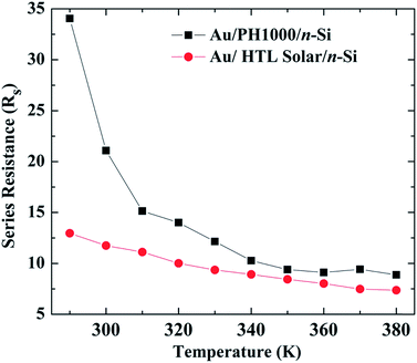 |
| | Fig. 6 Variation of series resistance with temperature determined from the Cheung equation. | |
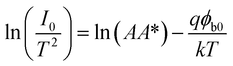
In order to find out the voltage dependent barrier height in forward bias I–V region is to make use of activation energy and Richardson constant can be written as:26
| |
 | (4) |
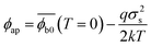
A conventional Richardson plot of ln(I0/T2) vs. 1000/T is shown in Fig. S2 in the ESI.† The activation energy and Richardson constant values are determined from the slop and intercept of the experimental Richardson plot and the values are much smaller than the known theoretical value for n-type Si. The above experimental results reveal that the low value of Richardson constant may be affected by the lateral inhomogeneity of the Gaussian distribution of barrier height. The above abnormal behavior can be explained using an analytical potential fluctuation model based on inhomogeneous barrier heights at the interface layer of PEDOT:PSS thin films between gold and n-type Si. Let us assume that the double Gaussian distribution of apparent BH (ϕap) with a mean barrier height ( ) and standard deviations (σs) can be expressed by the following relations:27,28
| |
 | (5) |
It is conceded that the mean BH,  and σs are linearly bias dependent on Gaussian parameters which may depend on temperature and quantify the voltage deformation of the barrier height distribution. Fitting of the experimental data into the eqn (5) Thus, we have attempted to draw a ϕap vs. 1000/T plot (Fig. S3 in the ESI†) to obtain the
  and σs at zero bias of a double Gaussian distribution of the BH. These results indicate the presence of a double Gaussian distribution of BH in the Schottky contact area. Now the modified conventional Richardson plot can be expressed as:29
| |
 | (6) |
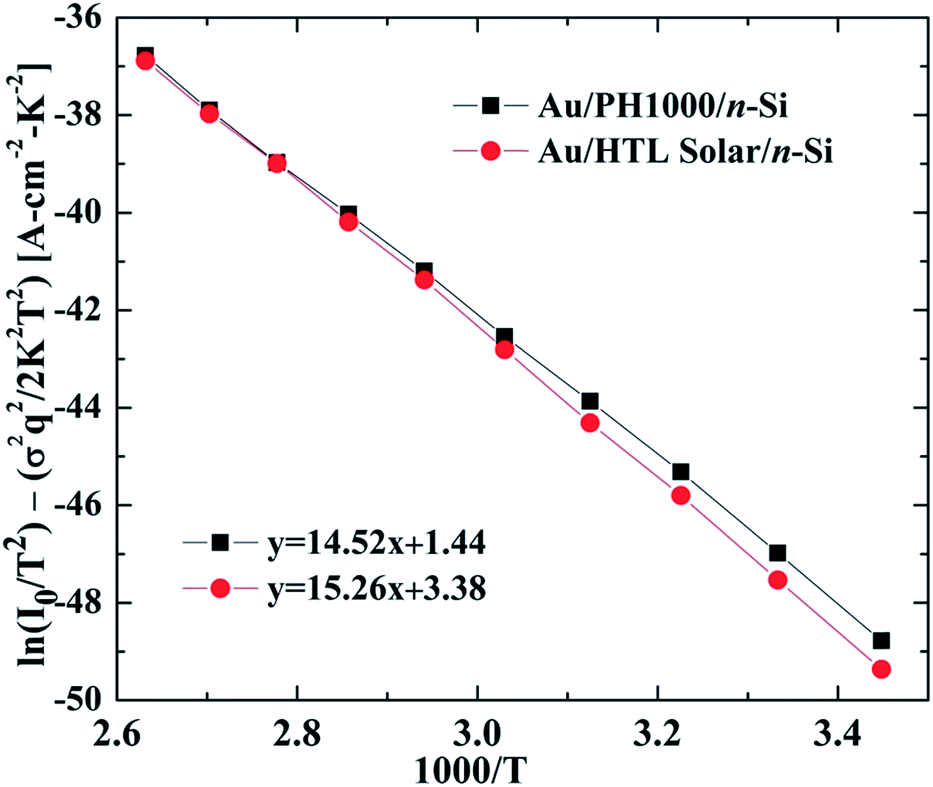
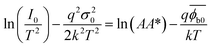
Thus the plot of modified activation energy according to eqn (6) should give a straight line. Slope which directly yields the mean barrier height ( ) and intercept (=lnAA*) at ordinate determine A* for a given diode area A. In Fig. 7, the modified ln(I0/T2) − (qσ)2/2(kT)2 vs. 1000/T plot gives
  and A* as 1.31 eV and 233.84 A cm−2 K−2 respectively for Au/HTL Solar/n-Si SBDs. It is cleared that the value of
  obtained from the modified activation energy plot is almost same as the value of
 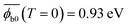 from ϕap vs. 1000/T plot. However the A* value is less for Au/PH1000/n-Si compare to the known theoretical value of 120 A cm−2 K−2 of n-type Si.
 |
| | Fig. 7 Modified Richardson ln(I0/T2) − (qσ)2/2(kT)2 vs. 1000/T plot of Au/PEDOT:PSS/n-Si SBDs of both PH1000 and HTL Solar products. | |
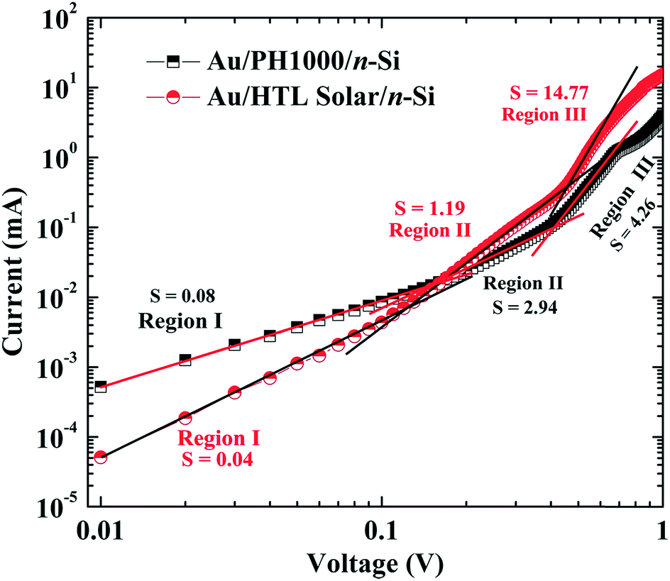
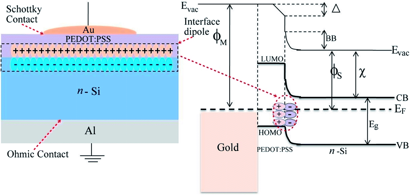
Finally, to compare the charge transport behavior through the interface layer of Au/PEDOT:PSS/n-Si SBDs can be obtained from the log(I)–log(V) plot of the I–V measurements. The variation of log(I) with log(V) for Au/PEDOT:PSS/n-Si SBDs is shown in Fig. 8. The curve shows three different regions of Au/PEDOT:PSS/n-Si SBDs indicating different conduction mechanisms in each region. In region (I), the injected effective charge carriers may be lower than the highly doped n-type Si. Therefore at the very low bias voltage the slope is less than 1 and the charge carriers are controlled by the trap. Thus the charge transport through the PEDOT:PSS thin film is controlled by the trapped-charge-limited current (TCLC). In region (II), the slope is greater than 1 and curve is a straight line that agrees with the Ohm's law and the current conduction mechanism is characterized by Ohm's law in this region. On the other hand in region (III) is characterized by power law where the slope is very high (>4). In this region the injection of charge carriers through the trap from the PEDOT:PSS is increased considerably because of the high bias voltage and formed an interface dipole at the junction. Fig. 9 shown the schematic diagram and band structure of PEDOT:PSS/n-Si Schottky junction. It is also found that the slope (region III) of HTL Solar is more compare to PH1000 product that indicates better rectification property justified the above explanation.
 |
| | Fig. 8 Forward bias log(I)–log(V) characteristics of Au/PH1000/n-Si and Au/HTL Solar/n-Si SBDs. ‘S’ is the slope of the curve. | |
 |
| | Fig. 9 (a) Schematic diagrams and (b) band diagram of Au/PEDOT:PSS/n-Si Schottky barrier diodes (SBDs) where BB is band bending, ϕM and ϕS is the work function of meal and semiconductor, χ is the electron affinity and Δ is the induced molecular dipole. | |
4. Conclusion
In summary, two commercial products of PEDOT:PSS solutions, PH1000 and HTL Solar were investigated their chemical composition, surface morphology and electrical properties. The XPS analysis demonstrated the PSS content in HTL Solar is more compared to PH1000 product, which was responsible for better passivation and stronger interface dipole formed between gold and n-type Si. The performance of Au/HTL Solar/n-Si SBDs was better due to high rectification property, low leakage current, less ideality factor, high barrier height and low series resistance compared to Au/PH1000/n-Si SBDs. Therefore, the excellence of HTL Solar product could enhance the performance of other semiconductor device applications.
Conflicts of interest
The author declares that there is no conflict of interest.
Acknowledgements
The author is thankful to Dr Ramkrishna Dev Das of Saha Institute of Nuclear Physics (Surface Physics and Material Science division), Kolkata, India for AFM measurement. The author is also grateful to Prof. Joaquim Puigdollers of Department of Electronic Engineering, Universitat Politècnica de Catalunya, Barcelona, Spain for his endless supports.
References
- K. Sun, S. Zhang, P. Li, Y. Xia, X. Zhang, D. Du, F. H. Isikgor and J. Ouyang, Review on application of PEDOTs and PEDOT:PSS in energy conversion and storage devices, J. Mater. Sci.: Mater. Electron., 2015, 26, 4438 CrossRef CAS
 .
. - Y. Zhang, W. Cui, Y. Zhu, F. Zu, L. Liao, S. T. Lee and B. Sun, High efficiency hybrid PEDOT:PSS/nanostructured silicon Schottky junction solar cells by doping-free rear contact, Energy Environ. Sci., 2015, 8, 297–302 CAS .
- X. Guo, X. Liu, F. Lin, H. Li, Y. Fan and N. Zhang, Highly Conductive Transparent Organic Electrodes with Multilayer Structures for Rigid and Flexible Optoelectronics, Sci. Rep., 2015, 5, 10569 CrossRef PubMed .
- A. K. Sarker, J. Kim, B. H. Wee, H. J. Song, Y. Lee, J. D. Hong and C. Lee, Hydroiodic acid treated PEDOT:PSS thin film as transparent electrode: an approach towards ITO free organic photovoltaics, RSC Adv., 2015, 5, 52019 RSC .
- M. Hokazono, H. Anno and N. Toshima, Thermoelectric Properties and Thermal Stability of PEDOT:PSS Films on a Polyimide Substrate and Application in Flexible Energy Conversion Devices, J. Electron. Mater., 2014, 43, 2196 CrossRef CAS .
- M. Eslamian, Inorganic and Organic Solution-Processed Thin Film Devices, Nano-Micro Lett., 2017, 9, 1 CrossRef .
- M. Singh, H. M. Haverinen, P. Dhagat and G. E. Jabbour, Inkjet Printing-Process and Its Applications, Adv. Mater., 2010, 22, 673 CrossRef CAS PubMed .
- K.-T. Park, H.-J. Kim, M.-J. Park, J.-H. Jeong, J. Lee, D.-G. Choi, J.-H. Lee and J.-H. Choi, 13.2% efficiency Si nanowire/PEDOT:PSS hybrid solar cell using a transfer-imprinted Au mesh electrode, Sci. Rep., 2015, 5, 12093 CrossRef CAS PubMed .
- W. Xu, Z. Hu, H. Liu, L. Lan, J. Peng, J. Wang and Y. Cao, Flexible All-organic, All-solution Processed Thin Film Transistor Array with Ultrashort Channel, Sci. Rep., 2016, 6, 29055 CrossRef CAS PubMed .
- H. M. Kim, J. Kim, J. Lee and J. Jang, Inverted Quantum-dot Light Emitting Diode Using Solution Processed p-Type WOx Doped PEDOT:PSS and Li Doped ZnO Charge Generation Layer, ACS Appl. Mater. Interfaces, 2015, 7, 24592 CAS .
- Y. J. Lin, B. C. Huang, Y. C. Lien, C. T. Lee, C. L. Tsai and H. C. Chang, Capacitance voltage and current–voltage characteristics of Au Schottky contact on n-type Si with a conducting polymer, J. Phys. D: Appl. Phys., 2009, 42, 165104 CrossRef .
- T. Tunç, Ş. Altindal, I. Uslu, I. Dökme and H. Uslu, Temperature dependent current–voltage(I–V) characteristics of Au/n-Si (111) Schottky barrier diodes with PVA (Ni,Zn-doped) interfacial layer, Mater. Sci. Semicond. Process., 2011, 14, 139 CrossRef .
- S. A. Yerişkin, M. Balbas and İkram Orak, The effects of (graphene doped-PVA) interlayer on the determinative electrical parameters of the Au/n-Si (MS) structures at room temperature, J. Mater. Sci.: Mater. Electron., 2017, 28, 7501 CrossRef .
- O. F. Yuksel, M. Kus, N. Simsir, H. Safak, M. Sahin and E. Yenel, A detailed analysis of current–voltage characteristics of Au/perylene-monoimide/n-Si Schottky barrier diodes over a wide, temperature range, J. Appl. Phys., 2011, 110, 024507 CrossRef .
- M. Wang, M. Zhou, L. Zhu, Q. Li and C. Jiang, Enhanced polymer solar cells efficiency by surface coating of the PEDOT:PSS with polar solvent, Solar Energy, 2016, 129, 175 CrossRef CAS .
- A. Österholma, T. Lindfors, J. Kauppila, P. Damlin and C. Kvarnström, Electrochemical incorporation of graphene oxide into conducting polymer films, Electrochim. Acta, 2012, 83, 463 CrossRef .
- P. W. Sze, K. W. Lee, P. C. Huang, D. W. Chou, B. S. Kao and C. J. Huang, The Investigation of High Quality PEDOT:PSS Film by Multilayer-Processing and Acid Treatment, Energies, 2017, 10, 716 CrossRef .
- A. Vilan and D. Cahen, Chemical Modification of Semiconductor Surfaces for Molecular Electronics, Chem. Rev., 2017, 117, 4624 CrossRef CAS PubMed .
- S. Mahato, L. G. Gerling, C. Voz, R. Alcubilla and J. Puigdollers, PEDOT:PSS as an Alternative Hole Selective Contact for ITO-Free Hybrid Crystalline Silicon Solar Cell, IEEE Journal of Photovoltaics, 2016, 6, 934 CrossRef .
- Y. J. Lin and J. H. Lin, Annealing effect on Schottky barrier inhomogeneity of graphene/n-type Si Schottky diodes, Appl. Surf. Sci., 2014, 311, 224 CrossRef CAS .
- S. M. Sze, Physics of Semiconductor Devices, Wiley, New York, 3rd edn, 1981 Search PubMed .
- M. A. Yeganeh and S. H. Rahmatollahpur, Barrier height and ideality factor dependency on identically produced small Au/p-Si Schottky barrier diodes, J. Semicond., 2010, 31, 074001 CrossRef .
- M. Sharma and S. K. Tripathi, Study of barrier inhomogeneities in I–V-T and C-V-T characteristics of Al/Al2O3/PVA:n-ZnSe metal–oxide semiconductor diode, J. Appl. Phys., 2012, 112, 024521 CrossRef .
- O. F. Yuksel, N. Tugluoglu, H. Safak and M. Kus, The modification of Schottky barrier height of Au/p-Si Schottky devices by perylene-diimide, J. Appl. Phys., 2013, 113, 044507 CrossRef .
- S. K. Cheung and N. W. Cheung, Extraction of Schottky diode parameters from forward current-voltage characteristics, Appl. Phys. Lett., 1986, 49, 85 CrossRef CAS .
- D. E. Yıldız, Ş. Altındal and H. Kanbur, Gaussian distribution of inhomogeneous barrier height in Al/SiO2/p-Si Schottky diodes, J. Appl. Phys., 2008, 103, 124502 CrossRef .
- A. Gumus, A. Turut and N. Yalcin, Temperature dependent barrier characteristics of CrNiCo alloy Schottky contacts on n-type molecular-beam epitaxy GaAs, J. Appl. Phys., 2002, 91, 245 CrossRef CAS .
- H. Tecimer, Ö. Vural, A. Kaya and Ş. Altındal, Current-transport mechanism in Au/V-doped PVC+TCNQ/p-Si structures, Int. J. Mod. Phys. B, 2015, 13, 1550076 CrossRef .
- S. Alialy, Ş. Altındal, E. E. Tanrıkulu and D. E. Yıldız, Analysis of temperature dependent current-conduction mechanisms in Au/TiO2/n-4HSiC (metal/insulator/semiconductor) type Schottky barrier diodes, J. Appl. Phys., 2014, 116, 083709 CrossRef .
Footnote |
| † Electronic supplementary information (ESI) available: Details calculation of series resistance and Richardson constant plot of Au/PEDOT:PSS/n-Si is used in this work. See DOI: 10.1039/c7ra10018c |
|
| This journal is © The Royal Society of Chemistry 2017 |
Click here to see how this site uses Cookies. View our privacy policy here. 
 Open Access Article
 This Open Access Article is licensed under a
  *
*
 is Richardson's constant and the value is 120 A cm−2 K−2 for n-type Si.22 The ideality factor and barrier height of the Schottky barrier diodes are describe the deviation of the experimental temperature dependent I–V data is expressed as:23,24
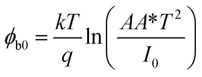


 ) and standard deviations (σs) can be expressed by the following relations:27,28
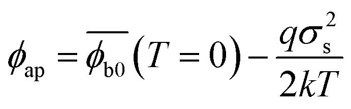
 and σs are linearly bias dependent on Gaussian parameters which may depend on temperature and quantify the voltage deformation of the barrier height distribution. Fitting of the experimental data into the eqn (5) Thus, we have attempted to draw a ϕap vs. 1000/T plot (Fig. S3 in the ESI†) to obtain the
  and σs at zero bias of a double Gaussian distribution of the BH. These results indicate the presence of a double Gaussian distribution of BH in the Schottky contact area. Now the modified conventional Richardson plot can be expressed as:29
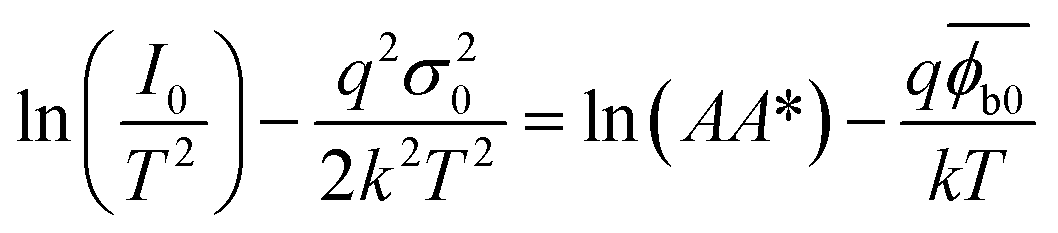
 ) and intercept (=ln
 and A* as 1.31 eV and 233.84 A cm−2 K−2 respectively for Au/HTL Solar/n-Si SBDs. It is cleared that the value of
 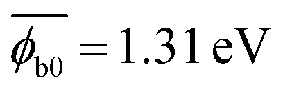 obtained from the modified activation energy plot is almost same as the value of
  from ϕap vs. 1000/T plot. However the A* value is less for Au/PH1000/n-Si compare to the known theoretical value of 120 A cm−2 K−2 of n-type Si.