
 Open Access Article
 This Open Access Article is licensed under a
 Creative Commons Attribution 3.0 Unported Licence
One-pot hydrothermal synthesis and selective etching method of a porous MoSe2 sand rose-like structure for electrocatalytic hydrogen evolution reaction†
Xuan Thai Tran,
Sujittra Poorahong and
Mohamed Siaj *
*
Department of Chemistry and Biochemistry, Université du Quebec à Montréal, Montréal, QC H3C 3P8, Canada. E-mail: siaj.mohamed@uqam.ca
First published on 10th November 2017
Abstract
The development of a platinum-free electrocatalyst for the hydrogen evolution reaction (HER) is highly essential to the large-scale production and application of water splitting devices. Herein we report a facile one-pot hydrothermal synthesis of composite MoSe2@Cu2Se. The morphology of the obtained material was characterized by scanning electron microscope (SEM) and it was found that the composite material formed a sand rose-like structure. The crystal structure and phase purity of the composite MoSe2@Cu2Se were investigated by X-ray diffraction (XRD) and transmission electron microscopy (TEM). Then a selective electrochemical etching of copper from the composite was carried out and the porous MoSe2 rose-like nanosphere was obtained. The robust 3D MoSe2 rose-like structure exhibit remarkable activity and durability for electrocatalytic HER in acid maintaining a small onset overpotential of ∼150 mV and keeping a small overpotential of 300 mV for 6 mA cm−2 current density after 1000 cycles. Based on our data, the obtained porous sand rose-like structure material could improve the active surface area which yields higher HER catalytic activity. The present study provides a simple and effective way for the exploration of efficient Mo-based HER catalysts.
Introduction
Hydrogen (H2) is a promising, clean, and renewable energy carrier to relieve our reliance on natural fossil fuels and can reduce the growing global greenhouse effects.1–3 Growing attention has been paid to the sustainable hydrogen evolution reaction (HER) from the water splitting reaction, which is a clean and environmentally benign reaction pathway.3,4 The most effective electrocatalyst for the HER in an acidic media is Pt group metals. However, several challenges remain in designing and selecting an electrocatalyst material. These are related to the expensiveness of Pt and low earth-abundance, which hinder its practical implementation.5,6 Limited surface active sites impede the HER from proceeding efficiently7 and chemical and structural stability issues of electrocatalysts in a harsh acidic environment were also another problem.8 These limitations have motivated several researchers to dedicate intensive efforts in designing and fabricating low-cost and plentiful HER electrocatalysts with high catalytic activities.9In recent years, many alternatives for non-precious metal-based electrocatalysts have been developed, including transition metal sulfides, selenides, borides, carbides, nitrides, phosphides, and a molecular catalyst family. Among all these alternatives a type of efficient electrocatalysts based on transition metal dichalcogenide (TMD) has recently received significant attention, because of its exotic electronic structure and these physical properties.10 TMD is a family of materials consisting of more than 40 compounds having the generalized formula MX2, wherein M is a transition metal, typically 4–7 groups and X is a chalcogen such as sulfur (S), selenium (Se) and tellurium (Te). These transition metals have an important catalytic behavior in the HER. The latter trend has formed with superimposed layers of weak interactions of van der Waals between two adjacent layers,10 this form has two large areas on the sides (active sites) for the adsorption of ions. It has been proven by further research that TMD slips active sites play an important role in HER. Among them, MoSe2 is a newly emerging catalyst owing to its low cost, high chemical stability, and excellent electrocatalytic activity.11–15 The electrocatalytic HER activity of MoSe2 depends strongly on its active selenium edge sites, while its basal planes were catalytically inert.16 In order to obtain, a high performance MoSe2 electrocatalyst towards the HER is to rationally construct the nanostructure for mass transfer and maximizing the number of active sites. A boost of the catalytic activities could be achieved by reducing the MoSe2 crystal size to nanoscale level and by increasing the exposures of its active edges to the electrolytes. In one aspect, a high surface area with an open structure avail the diffusion of electrolytes, will lead smoothly to the replenishment of the consumed protons and lower the ohmic drop at high reaction rate.17
Herein, we demonstrate the preparation of a 3D hierarchical porous MoSe2 by a combination of hydrothermal and chemical etching methods. To the best of our knowledge, here is the first report of the MoSe2@Cu2Se synthesis by hydrothermal method. After MoSe2@Cu2Se synthesis, the copper is selectively etched from the alloy leading to a 3D porous MoSe2 structure formation (sand rose-like structure). The 3D porous MoSe2 material is tested as a catalyst for HER. A comparison between pure MoSe2 and porous MoSe2 sand rose-like structure shows that the porous one exhibits higher catalytic activity for electrocatalytic HER.
Experimental
Synthesis porous MoSe2
The preparation procedure of Mo@Cu selenide composite is schematically described in Fig. 1. The Synthesis was carried out using 0.42 g of ammonium molybdate tetrahydrate, 0.6 g copper(II) sulfate pentahydrate and 1.065 g SeO2 powder in 20 mL of distilled water under vigorous stirring for 45 minutes to form a homogeneous solution. After that, 50 mL of ethylene diamine was added with stirring continuously for 15 min at room temperature. The final solution has given a greenish color. The solution was then transferred to a stainless-steel autoclave with 100 mL Teflon coated and maintained at 210 °C for 23 h; Fig. 1A. After the reaction, the system was cooled down to room temperature. The precipitated black obtained were collected by centrifugation at 4000 rpm for 15 minutes, washed with distilled water and ethanol at least 4 times, and then dried at 60 °C under vacuum. To yield the final crystalline products, the precipitate products were dried at 500 °C for 1 h in an atmosphere of argon (Ar). After that, the copper component was etched out from the composite under sonication in 0.5 M ammonium persulfate for 30 min. After the etching procedure, the porous MoSe2 sand rose-like structure was obtained (Fig. 1B). As a control experiment, the synthesis of pure MoSe2 and Cu2Se were prepared following the same method motioned above.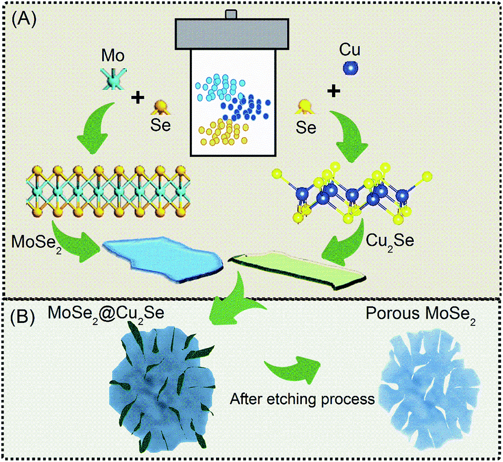 | ||
| Fig. 1 (A) The procedure of the MoSe2@Cu2Se powder synthesis. (B) The expected morphology after etching process. | ||
Electrochemical measurement
All electrochemical measurements were performed in a disposable three electrodes system (EP-PP, Biodevice Technology, Japan) consisted of a working electrode (carbon, 2 mm diameter), a counter electrode (carbon) and a reference electrode (Ag/AgCl). The electrochemical experiments were performed at room temperature and were carried out using SP-300 potentiostat (Bio-Logic Science Instrument, France) connected to a personal computer and driven by EC-Lab software. Prior to all electrochemical measurements, 60 mg of porous MoSe2 product and 150 μL of Nafion solution (Sigma Aldrich, 5 wt%) was dispersed in a 5 mL water-ethanol solution with a volume ratio of 4![[thin space (1/6-em)]](https://www.rsc.org/images/entities/char_2009.gif) :1 by at least 30 min sonication to from a homogeneous ink. Finally, 3 μL of as-prepared slurry (containing 35 μg of catalyst) was dropped on to the carbon-working electrode. Finally, the as-prepared catalyst film was dried in the air at room temperature.
:1 by at least 30 min sonication to from a homogeneous ink. Finally, 3 μL of as-prepared slurry (containing 35 μg of catalyst) was dropped on to the carbon-working electrode. Finally, the as-prepared catalyst film was dried in the air at room temperature.
Linear sweep voltammetry (LSV) was performed in 0.5 M H2SO4 saturated using an Ag/AgCl as the reference electrode, and a carbon as the counter electrode. All the potentials were calibrated to a reversible hydrogen electrode (RHE). LSV was recorded by sweeping the potential from 0.2 to −0.8 V vs. RHE with a scan rate of 1 mV s−1 at room temperature. Cyclic voltammetry (CV) was conducted for 1000 cycles between 0.1 V to −0.8 V (vs. RHE) at 100 mV s−1 for the stability test. The Nyquist plots were measured with frequencies ranging from 200 kHz to 100 mHz at an overpotential of −250 mV. The impedance data were then plotted to a simplified Randles circuit to extract the series and charge-transfer resistances.
Characterization
The X-ray diffraction (XRD) was performed using a diffractometer (Bruker D8 Advance) with Cu-Kα radiation (λ = 1.54182 Å) at room temperature. X-ray photoelectron spectroscopy (XPS) data for elemental composition and valence information was collected with XPS PHI 5600-ci (Physical Electronics, Eden Prairie, MN, USA). Scanning electron microscope was recorded on JEOL (JSM7600F) with an accelerating voltage of 10 kV and a working distance of 5 mm using secondary electron imaging mode. Raman spectra of the films were recorded with alpha300 R Confocal Raman Microscope with WITec UHTS 300 spectrometer with a 532 nm laser. Transmission electron microscopy (TEM) and Energy-dispersive X-ray spectroscopy (EDS) was performed on a Joel JEM-2100F.Results and discussion
Structure and morphology of porous MoSe2
The crystallographic structures and phase purity of as-prepared materials were determined by XRD. Fig. 2A-(i), shows the diffraction peaks in the two-theta range of 10–80° which implies the crystalline nature of the obtained materials. The asymmetric-shaped and broadening diffraction peaks, which are the typical features of 2D nanosheets, demonstrate that the MoSe2 rose-like structure is completely comprised of layered flakes.12 All of these diffraction peaks are in good agreement with the characteristic planes i.e., (002), (100), (103) and (110) of the hexagonal MoSe2 phase (JCPDS 29-0914), revealing the high purity of the as-synthesized product. In the case of copper selenide synthesis, Fig. 2A-(ii), the XRD patterns exhibit well-defined peaks which were indicated with the standard pattern of Cu2Se (JCPDS no. 01-088-2043). Fig. 2A-(iii) shows the XRD pattern of the composite Mo@Cu selenide. It can be seen that all diffraction peaks in the MoSe2@Cu2Se composite the X-ray diffraction patterns can be separated from the compounds either MoSe2 or Cu2Se, demonstrating a phase purity of the synthesized product. In addition, the peaks compatible with those indicated by the virgin MoSe2 are enlarged. These characteristics show that the Cu2Se compound tends to aggregate and form larger sizes, while MoSe2 retains its nanometric size distribution in the MoSe2@Cu2Se composite. After etching processes, the XRD pattern of Cu2Se disappeared, showing only the pattern corresponding to MoSe2 (Fig. 2A-(iv)). From the XRD result, it can be concluded that the Cu2Se was successfully eliminated.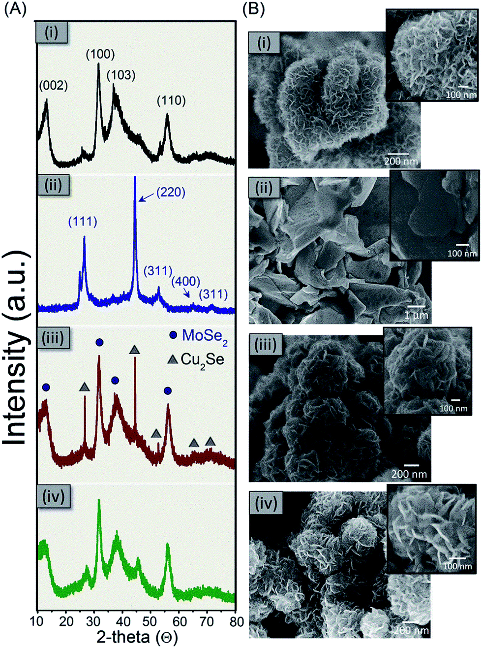 | ||
| Fig. 2 (A) The XRD pattern and (B) the SEM morphology of the as-prepared materials grown by solvothermal method (i) MoSe2, (ii) Cu2Se, (iii) MoSe2@Cu2Se and (iv) porous MoSe2 after etching the Cu2Se. | ||
Fig. 2B-(i) presents the morphology of pure MoSe2 produced by the solvothermal process involving (NH4)6Mo7O24·4H2O as the Mo source and SeO2 as the Se source. The morphology of pristine MoSe2 can be described as the rose-like microsphere that consists of a large number of petals. While Cu2Se has an irregular morphology in the form of dense nanoplates and/or nanocrystals, Fig. 2B-(ii). Even though pure MoSe2 and composite MoSe2@Cu2Se have rose-like microsphere morphology, the petals of pure MoSe2 are thinner than that from MoSe2@Cu2Se composite. Also, compared spaces between the petals of the material composite are denser than MoSe2. Fig. 2B-(iv) shows SEM images indicate that after etching the composite of the rose-like structures remains intact with more porous and opened structure. Such enormous nanosheets could provide a large number of active sites accompanied with a large specific surface area. The dispersion homogeneity of the different components is supported by the selected element mapping of Mo, Cu and Se (ESI Fig. S1†). The mapping of MoSe2@Cu2Se composite sample demonstrates clearly the existence of each element, in addition to being well distributed over the composite material. After the etching process, no copper element was detected. This mapping confirms that the etching process has been done successfully.
The low-resolution TEM images in Fig. 3A and B indicate the rose-like structure formation of porous MoSe2. High-resolution transmission electron microscopy (HRTEM) images of the MoSe2 reveal the microscopic phase information as well as the thickness of the MoSe2. It can be seen that each section of the nanoflowers presenting a shape of a petal is actually an individual stack of 2D MoSe2 thin layers. A large amount of active sites can be attributed to widely distributed petals, which would offer much more active sites for HER. The spacing between two adjacent monolayers is 0.277 nm, which is consistent with the value of MoSe2 interlayer spacing of the (100) plane (Fig. 3C). The selected area electron diffraction (SAED) results also reflect the (002) planes of 2H-MoSe2 clearly in the inset Fig. 3C. Fig. 3D shows the other plane of MoSe2 obtained from the average values for five layers is 0.72 nm, in good accordance with the thickness of the atomic layer of Se–Mo–Se unit where the c-axis orients normal to the (002) lattice plane. Therefore, we conclude that the MoSe2 porous microspheres are composed of MoSe2 monolayer flakes in an incompact way. Furthermore, the comparison between TEM images of pure MoSe2 (ESI Fig. S2A†) and MoSe2 after etching process (ESI Fig. S2B†), the pure MoSe2 looks denser than those MoSe2 after etching. On the other word, after took Cu2Se out from composite material, MoSe2 becomes hollow. To prove that the specific area increased indeed, Brunauer–Emmett–Teller (BET) method was used to measure the surface area of the pure and etched MoSe2. ESI Fig. S3A† shows nitrogen adsorption and desorption isotherms for the porous MoSe2 sample. It showed a hysteresis loop curve, which is the characteristic of a mesoporous material. BET specific surface area for the porous MoSe2 sample was 33.59 m2 g−1 while that the porous MoSe2 was only 12.31 m2 g−1. So, the surface area of the composite increased by about 2.72 times compared with pure MoSe2. Then the density functional theory (DFT) was applied to calculate the pore size distribution from the adsorption isotherm. As you can see in ESI Fig. S3B,† the material possesses the micropores characteristic from the range of 23–54 Å. It has been expected that the relatively large surface area of the as-prepared porous MoSe2 rose-like microspheres not only can provide more active sites but also enhance the conductivity, which may improve the performance for a further application.
 | ||
| Fig. 3 (A and B) TEM images porous MoSe2 under different magnifications. (C) HRTEM image of an area of the surface of MoSe2; inset the selected area electron diffraction profile. (D) Plot of the calibration for measuring the spacing and the corresponding atomic stacking models. | ||
Then the Raman spectroscopy of all samples has been carried out. The observation of the Raman spectra of MoSe2 (Fig. 4A-(i)) can be noted that there are two resonance peaks at 238 cm−1 and 283 cm−1 which can be well indexed to the out-of-plane A1g and in-plane E12g modes of 2H-MoSe2, respectively.18 In the Cu2Se Raman spectrum (Fig. 4A-(ii)), an active mode A1g at 257 cm−1 is observed. It is corresponding to Cu–Se vibration and is in good agreement with the literature.19 In the Raman spectrum of MoSe2@Cu2Se composite (Fig. 4A-(iii)), it can be noted that the two-mode vibration at 237 cm−1 MoSe2 and at 256 cm−1 Cu2Se appears in this spectrum. After the etching process (Fig. 4A-(iv)), the sample exhibits two Raman peak at 237.1 cm−1 and 283.1 cm−1. In addition, as can be seen, the A1g peak intensity is much higher than the E12g peak at pure MoSe2 and MoSe2 composite. This Raman peak corresponding to the out-of-plane Mo–Se phonon mode is preferentially excited for the edge-terminated perpendicularly-oriented nanosheets.11 Moreover, after etching process, the E12g peak intensity is much higher than A1g peak where the E12g peak is preferentially excited for terrace-terminated film. It can be supported the porous structure MoSe2 formation. These make a relatively weak layer–layer interactions in the porous MoSe2 nanosheets happen and in-plan Mo–Se phonon occurs. Photoluminescence spectroscopy was used to investigate the optical emission properties of porous MoSe2. As shown in ESI Fig. S4† the porous MoSe2 shows bandgap energy of 1.54 eV.
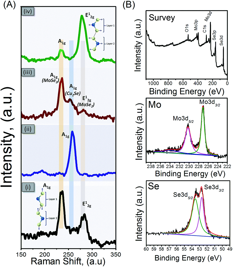 | ||
| Fig. 4 (A) Raman spectra of (i) MoSe2, (ii) Cu2Se , (iii)MoSe2@Cu2Se and (iv) porous MoSe2 after etched Cu2Se; inset the atomic vibration manners of the A1g and E12g vibrational modes of MoSe2. Blue and yellow balls represent Mo and Se atoms, respectively. (B) XPS survey and high-resolution spectra showing the binding energies of Mo 3d and Se 3d of porous MoSe2. | ||
Chemical compositions on the surface and valence states of the porous MoSe2 rose-like microspheres were further investigated by X-ray photoelectron spectroscopy (XPS) measurements. Fig. 4B shows the XPS survey spectrum of MoSe2 after etched Cu2Se out. In which the peaks derived from Mo, Se, C and O elements were detected; no Cu peak was observed compared to composite materials sample (ESI Fig. S5†). Generally, a small amount of oxygen may be due to surface adsorption of oxygen, and the C 1s peak located at 284.6 eV mainly results from the contamination from the used carbon conductive tabs. The core-level XPS spectra of Mo 3d shows the binding energies at 229 eV and 232.1 eV belong to Mo 3d5/2 and 3d3/2 spin orbit peaks of MoSe2, confirming the elemental chemical state of Mo is mainly the Mo4+ oxidation state in the hexagonal 2H phase of MoSe2. In case of Se, two fitted peaks at 55.4 and 54.5 eV attributable to the core levels of Se 3d3/2 and Se 3d5/2, respectively, are further illustrating Se2− of the MoSe2.
All of the above characterization results prove that the hybrid MoSe2@CuSe2 is the individual compound and formation can be described as followed. Under the solvothermal condition, as the temperature and pressure increase, Mo(VI) reduced to Mo(IV) by C2H8N2 and then reacts with Se from the decomposition of SeO2 to form MoSe2. At the same time, the Cu2Se nanoparticles also form via stacking of a redox reaction occurred between the copper and the Sex2− to form Cu2Se crystal.19 The generated MoSe2 and Cu2Se nucleus accumulates and leads to nanosheets growth. With the increasing time, the nanosheets of both materials tend to aggregate to form 2D layer and several layers stack under the influence of the hydrogen bonding interaction and thermodynamic stability20 and finally formed 3D hierarchical microsphere-like of composite MoSe2@Cu2Se. As resulting in the elements are well distributed over the composite material. Furthermore, the etching process does not inhibit the MoSe2 properties.
Electrocatalytic analysis
The as-prepared porous MoSe2 rose-like microspheres combine the advantages of the intrinsic properties of 2D MoSe2 monolayer flakes and the 3D porous structures, which are believed to greatly benefit their applications. Here, we investigate their electrocatalytic activity for HER in acid. HER is the key process to electrolytic or photoelectrochemical water splitting. The search for efficient and robust HER electrocatalysts is at the heart of clean energy research. To investigate the HER performance of the synthesized porous MoSe2, the electrochemical measurements were carried out in a N2-saturated 0.5 M H2SO4 at room temperature using a three-electrode cell. For comparison, HER catalytic measurement using MoSe2, Pt and bare carbon have been conducted in the same conditions. Fig. 5A shows the polarization curves of the current density (J) versus the potential of the pure MoSe2 and porous MoSe2 synthesis, bare carbon and commercial Pt catalysts. Toward the negative potential direction, cathodic waves rise due to the electrocatalytic reduction of proton to H2. For porous rose-like microspheres, onset overpotential of ∼150 mV vs. RHE is recorded, corresponding to a small HER overpotential of ∼300 mV for 6 mA cm−2 current density. However, pure MoSe2 exhibits a clear inferior electrocatalytic activity compared to MoSe2 rose-like microspheres. It is worth noting that monolayer flakes are significantly worse with an onset overpotential about −400 mV. We assume that the severe aggregation of monolayer flakes during electrocatalysis leads to the diminished surface areas and thus the poor HER performance. In this work the electrochemical performance of MoSe2@Cu2Se composite was not studied. This is due to Cu2Se is able to oxidize in the potential range for HER study. So it can affect HER results. In addition, the distinguished catalytic performance of 3D porous structure of MoSe2 is also indicated by the exceptionally low Tafel slope of ∼56 mV per decade (Fig. 5B). In comparison with the 3D porous structure, higher Tafel slops of MoSe2 compacted spheres (pure MoSe2) was measured as ∼71 mV per decade. We attribute these merits to the 3D porous structures of MoSe2 rose-like microspheres which retain excellent structure rigidity and possess more catalytic sites during electrocatalysis. In the present work, the Tafel slope is 56 mV per decade for the porous MoSe2 (rose-like structure), illustrating the Heyrovsky reaction plays a dominant role in determining the HER rate of this catalyst material. The Tafel slope in this work is indeed close to the values of 3D MoS2/MoSe2 nanosheet-graphene networks (61 mV per decade),16 MoS2/MoSe2 host lattice (50–60 mV per decade)21 MoSe2/carbon fiber aerogel hybrids (62 mV per decade)22 and compositing MoSe2 on MoS2 (65 mV per decade).23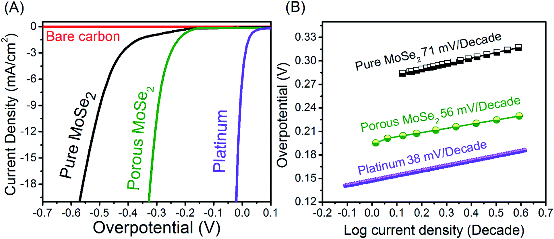 | ||
| Fig. 5 Electrochemical measurements of MoSe2 products. (A) Polarization curves and (B) corresponding Tafel plots obtained from the polarization curve of MoSe2 porous microspheres in 0.5 M H2SO4 along with the bare carbon, pure MoSe2 and platinum electrodes. | ||
Impedance spectroscopy (Fig. 6A) revealed that the pure MoSe2 films themselves contributed significantly to the series resistance in addition to the substrate and solution resistances. Consequently, this may contribute to the observed trends in turnover frequency. The high degree of resistance from the pure MoSe2 is not surprising, given that MoSe2 possesses semiconducting as well as anisotropic charge transport properties. However, the charge transfer resistance of the porous MoSe2 was much smaller. The material showed a charge transfer resistance of about 150 Ω. These results suggest that the conductivity of the porous MoSe2 is much higher than that of pure MoSe2, which indicates a much faster electron transfer process during electrochemical reaction. Other than high electrocatalytic activity, good durability is another important criterion in the selection of electrocatalysts. Here, MoSe2 porous microsphere catalyst was continuously cycled for 1000 times in 0.5 M H2SO4. The polarization curves before and after 1000 cycles were compared as shown in Fig. 6B. Little HER activity loss is discernible, indicating that the 3D porous structure of MoSe2 rose-like microspheres is highly stable and no significant electrocatalytic active sites were lost during the cycles.
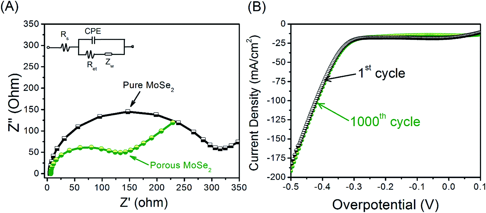 | ||
| Fig. 6 (A) EIS Nyquist plots of pure MoSe2 and porous MoSe2. (B) Polarization curves of MoSe2 porous microsphere catalyst before and after 1000 potential cycles in 0.5 M H2SO4. | ||
Conclusions
We have demonstrated a simple and rational method to provide a significant enhancement of the electrocatalytic performance of porous rose-like MoSe2 structure by a combination of hydrothermal and chemical etching methods. This new approach leads to favorable kinetics, metallic conductivity, and proliferation of active sites in a unique 3D architecture of 2H-MoSe2. Benefiting from the 3D porous structures, the electrocatalytic profiles of the MoSe2 rose-like microspheres as a catalyst for hydrogen evolution is evaluated, of which the result proves the excellent HER catalytic performance and good durability of 3D porous microspheres MoSe2. We expect that this facile methodology could be expanded to prepare more 3D porous structures comprising their monolayered units, which will open new opportunities in exploring their undiscovered properties and applications.Conflicts of interest
There are no conflicts to declare.Acknowledgements
This work was supported through funding from the Natural Science and Engineering Research Council of Canada (NSERC), the Canada Research Chairs program (CRC) and Canada Foundation for Innovation. We acknowledge all the characterization centers including NanoQAM, Le Centre de Caractérisation Microscopique des Matériaux (CM2) and Laboratoire de Caractérisation des Matériaux (LCM). We also thank Pr Daniel Belanger (UQAM) for the discussion about the electrochemical measurements.References
- L. Schlapbach and A. Zuttel, Nature, 2001, 414(6861), 353–358 CrossRef CAS.
- J. A. Turner, Science, 2004, 305(5686), 972–974 CrossRef CAS PubMed.
- M. S. Dresselhaus and I. L. Thomas, Nature, 2001, 414(6861), 332–337 CrossRef CAS PubMed.
- N. S. Lewis and D. G. Nocera, Proc. Natl. Acad. Sci. U. S. A., 2006, 103(43), 15729–15735 CrossRef CAS PubMed.
- J. Greeley, T. F. Jaramillo, J. Bonde, I. Chorkendorff and J. K. Norskov, Nat. Mater., 2006, 5(11), 909–913 CrossRef CAS PubMed.
- M. Wang, L. Chen and L. Sun, Energy Environ. Sci., 2012, 5(5), 6763–6778 CAS.
- V. W.-h. Lau, A. F. Masters, A. M. Bond and T. Maschmeyer, Chem.–Eur. J., 2012, 18(26), 8230–8239 CrossRef CAS PubMed.
- K. Rakstys, A. Abate, M. I. Dar, P. Gao, V. Jankauskas, G. Jacopin, E. Kamarauskas, S. Kazim, S. Ahmad, M. Grätzel and M. K. Nazeeruddin, J. Am. Chem. Soc., 2015, 137(51), 16172–16178 CrossRef CAS PubMed.
- Y. Zheng, Y. Jiao, M. Jaroniec and S. Z. Qiao, Angew. Chem., 2015, 54(1), 52–65 CrossRef CAS PubMed.
- M. Chhowalla, Z. Liu and H. Zhang, Chem. Soc. Rev., 2015, 44(9), 2584–2586 RSC.
- S. Mao, Z. Wen, S. Ci, X. Guo, K. Ostrikov and J. Chen, Small, 2015, 11(4), 414–419 CrossRef CAS PubMed.
- Y. Zhang, Q. Gong, L. Li, H. Yang, Y. Li and Q. Wang, Nano Res., 2015, 8(4), 1108–1115 CrossRef CAS.
- X. Hu, W. Zhang, X. Liu, Y. Mei and Y. Huang, Chem. Soc. Rev., 2015, 44(8), 2376–2404 RSC.
- J. C. Shaw, H. Zhou, Y. Chen, N. O. Weiss, Y. Liu, Y. Huang and X. Duan, Nano Res., 2014, 7(4), 511–517 CrossRef CAS.
- L. Jia, X. Sun, Y. Jiang, S. Yu and C. Wang, Adv. Funct. Mater., 2015, 25(12), 1814–1820 CrossRef CAS.
- S. Xu, Z. Lei and P. Wu, J. Mater. Chem. A, 2015, 3(31), 16337–16347 CAS.
- H. Huang, L. Chen, C. Liu, X. Liu, S. Fang, W. Liu and Y. Liu, J. Mater. Chem. A, 2016, 4(38), 14577–14585 CAS.
- D. Kong, H. Wang, J. J. Cha, M. Pasta, K. J. Koski, J. Yao and Y. Cui, Nano Lett., 2013, 13(3), 1341–1347 CrossRef CAS PubMed.
- F. Lin, G.-Q. Bian, Z.-X. Lei, Z.-J. Lu and J. Dai, Solid State Sci., 2009, 11(5), 972–975 CrossRef CAS.
- C. Dai, E. Qing, Y. Li, Z. Zhou, C. Yang, X. Tian and Y. Wang, Nanoscale, 2015, 7(47), 19970–19976 RSC.
- V. Kiran, D. Mukherjee, R. N. Jenjeti and S. Sampath, Nanoscale, 2014, 6(21), 12856–12863 RSC.
- Y. Zhang, L. Zuo, L. Zhang, Y. Huang, H. Lu, W. Fan and T. Liu, ACS Appl. Mater. Interfaces, 2016, 8(11), 7077–7085 CAS.
- X. Lei, K. Yu, H. Li, Z. Tang and Z. Zhu, J. Phys. Chem. C, 2016, 120(28), 15096–15104 CAS.
Footnote |
| † Electronic supplementary information (ESI) available: One-pot hydrothermal synthesis and selective etching method of porous MoSe2 sand rose-like structure for electrocatalytic hydrogen evolution reaction. See DOI: 10.1039/c7ra10001a |
| This journal is © The Royal Society of Chemistry 2017 |