
 Open Access Article
 This Open Access Article is licensed under a Creative Commons Attribution-Non Commercial 3.0 Unported Licence
Robust quasi-ohmic contact against angle rotation in noble transition-metal-dichalcogenide/graphene heterobilayers
Siyao Houa,
Lihong Hana,
Liyuan Wua,
Ruge Quhe *ab and
Pengfei Lu*ac
*ab and
Pengfei Lu*ac
aState Key Laboratory of Information Photonics and Optical Communications, Beijing University of Posts and Telecommunications, Beijing 100876, China. E-mail: quheruge@bupt.edu.cn; photon@bupt.edu.cn
bSchool of Science, Beijing University of Posts and Telecommunications, Beijing 100876, China
cState Key Laboratory of Functional Materials for Informatics, Shanghai Institute of Microsystem and Information Technology, Chinese Academy of Sciences, Shanghai 200050, China
First published on 26th September 2017
Abstract
Stacked 2D crystals provide great possibilities to achieve desired functionalities with varying thickness and composition properties. In this work, the electronic properties of heterobilayers of noble transition-metal-dichalcogenide (PdS2, PtS2)/graphene with interlayer rotation angles are systematically investigated by density functional theory calculations. The two layers are combined by weak van der Waals interactions. Each component preserves its band structure in the hybrid system. A charge transference occurs at the interface of the bilayers leading to p-type doping for graphene and n-type doping for PdS2 (PtS2). Schottky barriers ranging from 0 eV to 0.057 eV appear in both heterobilayers with different orientations between the two monolayers. These results suggest that PdS2 (PtS2)/graphene heterobilayers have quasi-ohmic contact against interface angle rotation.
1. Introduction
Since the successful invention of isolated graphene in experiments, two-dimensional (2D) materials have received much attention.1–5 Layered transition-metal dichalcogenide (TMDC) nanostructures, which consist of one layer of transition metal atoms (Mo, W, V, or Ti) sandwiched between two layers of chalcogen atoms (S, Se, or Te), are now rapidly emerging, as they display unique chemical and physical properties that are absent or difficult to obtain in other 2D materials.6 As many TMDCs are inherent semiconductors by nature, a wide range of TMDC based applications in electronics, optoelectronics, photovoltaics, and catalysis have been demonstrated.7–13 While intensive interests are focused on MoS2 and WSe2, a new type of TMDC, noble-transition-metal dichalcogenides (nTMDCs), remains rarely explored, and understanding the physics behind this system is fundamental to their practical applications. The pioneering work by Grønvold et al. indicates that the noble metals Pt and Pd can form layered structures with S atoms.14–16 These monolayer noble-transition-metal disulfides MS2 (M = Pt and Pd) are typical semiconductors with indirect band gaps of 1.75 eV for PtS2 and 1.11 eV for PdS2.17 The PtS2 crystal has a layer-dependent indirect bandgap from 1.6 eV (monolayer) to 0.25 eV (bulk).18 Moreover, the phonon-limited mobility of platinum disulfide (PtS2) can be as high as 1107 cm2 V−1 s−1 at room temperature, about four times the carrier mobility of MoS2.19 Therefore, PtS2 may show better performance than MoS2 when it serves as a channel in field effect transistors (FETs).Recent efforts have focused on taking advantage of the individual properties of different 2D materials by fabricating heterostructures, which are vertical stacks of 2D layers of dissimilar materials held together by van der Waals (vdW) forces.20 Graphene is an ideal component of multilayer heterojunctions including graphene/silicene, graphene/hexagonal boron nitride, graphene/stanene, graphene/phosphorene, and graphene/MoS2,21–26 due to its high stability and outstanding electronic properties. Such heterostructures may lead to the opening of a bandgap in graphene without impairing its electronic mobility.27–29 Moreover, graphene is a suitable source electrode for TMDC based FETs. PtSe2/G has a tunable layer-dependent Schottky barrier.30 The traditional backgate MoS2 field effect transistor with ion gel dielectrics has a rather low carrier mobility of 0.5–20 cm2 V−1 s−1, while the characteristics of high mobility from graphene and high on-off ratio from MoS2 are properly balanced in the MoS2/graphene heterojunction based FET with an on–off ratio of 105 and a carrier mobility of 58.7 cm2 V−1 s−1.31–33 Different interlayer orientations might form in the synthesis of multilayer 2D materials, and interlayer orientation may affect the electronic properties.34–41 To the best of our knowledge, the influence of interlayer rotation on the electronic properties of nTMDC/graphene hybrids is unknown.
In this paper, we have investigated the structure and electronic properties of nTMDC/graphene heterojunctions (PdS2/G and PtS2/G). Furthermore, we study the effect of interlayer orientation between two different 2D materials as a tuning parameter for the electronic properties of the bilayer heterostructure. The relative orientation of graphene with respect to the MS2 layer apparently influences the interlayer spacing and the binding energy, but only slightly influences the value of the bandgap in MS2. Robust quasi-ohmic contact against angle rotation is found in both PtS2/G and PdS2/G heterostructures.
2. Methods and computational details
Our calculations were performed using the Vienna ab initio simulation package (VASP) within the framework of the plane-wave pseudopotential DFT method.42,43 The ion–electron interactions were described by the projected augmented wave method (PAW), and the generalized gradient approximation of Perdew, Burke, and Ernzerhof (PBE) was employed to describe the exchange–correlation interactions.44–47 In addition, the van der Waals interactions were considered using the DFT-D2 method.48 The Brillouin zone was sampled by a k-point mesh of 0.05 Å−1 separation in reciprocal space within the Monkhorst–Pack scheme, and the kinetic energy cutoff was chosen to be 400 eV.49 A vacuum region larger than 15 Å was added to avoid spurious interactions between periodic images. All atomic positions were fully optimized until the forces acting on each atom were less than 0.01 eV Å−1.Twisted bilayers were modeled using accidental angular commensurations.50 In a hexagonal lattice whose basis vector is a1 and a2, a skewed supercell with a basis vector (na1 + ma2) has a corresponding skewed angle,  . The MS2/G hybrid sheets were designed by looking for pairs of commensurate skewed cells of the two lattices with similar periodicity. The rotation angle of graphene relative to PdS2 (PtS2) can be expressed as θG − θMS2, namely the angle between the two zigzag directions, as shown in Fig. 1. Heterostructures are modeled by expanding the two monolayer unit cells to search the proper lattice combinations. To reduce the impact of external strain on MS2 as much as possible, we chose the MS′2 lattice parameter as the lattice parameter of the studied system when modeling the heterostructures. To avoid a large amount of computation and to sustain the original stability of the atom layers, we searched the combinations which could reach the balance between a little mismatch and a small number of atoms. We restricted the mismatch range from −5% to 5%. In this way, we found six twisted superstructures with relatively smaller numbers of atoms, namely,
  . In these superstructures, the number of atoms inside the unit cell increases as the orientation angle increases. In order to study the difference between the zigzag (ZZ) direction and the armchair direction (AC), we need a superstructure where the AC direction of graphene coincides with the ZZ direction of the MS2 layer. However, to reduce the computational complexity, we adopted four typical superstructures as shown in Fig. 1, namely,
  , corresponding to rotation angles of 0, 7.3, 13.9 and 30, respectively. The interlayer displacement is confined to a stacking order where a C atom of graphene and a S atom of MS2 are superimposed within each unit cell, considering that the interlayer bonding is insensitive to their mutual translation.
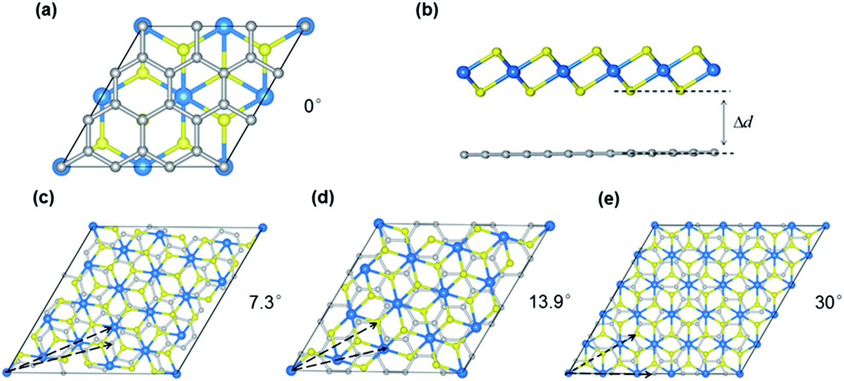 | ||
| Fig. 1 Atomic geometries of the MS2/G heterobilayer (M = Pt, Pd). (a and c–e) Top views of MS2/G with rotation angles of 0, 7.3, 13.9 and 30 degrees, respectively. (b) Side view of the MS2/G heterojunction, Δd indicates the interlayer distance between the two monolayers. The yellow, blue and silver spheres indicate sulfur, M and carbon atoms, respectively. | ||
3. Results and discussions
3.1 Structure and energetics
The key geometrical properties of the two 1 × 1 non-twisted configurations are listed in Table 1. For PtS2/G, the lowest S atom layer lies about 3.51 Å below the graphene. For PdS2/G, the interface distance is about 3.45 Å. These interlayer distance values are close to those of the van der Waals systems such as graphite. Therefore, we infer that the interactions between graphene and PtS2 or PdS2 in the heterostructures are relatively weak. The interlayer distance has little change when the orientation is considered in a range of 0.01 Å, and this is very similar to twisted MoS2/graphene heterobilayers.41 To quantitatively evaluate the interlayer interaction in the heterojunction, we calculated the binding energy (Eb), based on the following equation:| Eb = (EG + EMS2 − EMS2/G)/NC |
| θ (°) | a (Å) | Mismatch | Δd (Å) | h (Å) | ΦTB (eV) | |
|---|---|---|---|---|---|---|
| PtS2/G | 0 | 7.19 | −2.3% | 3.51 | 2.65 | 3.95 |
| 7.3 | 15.66 | 1.9% | 3.51 | 2.72 | 4.23 | |
| 13.9 | 12.95 | 1.4% | 3.55 | 2.66 | 3.75 | |
| 30 | 17.96 | 5.2% | 3.51 | 2.66 | 4.40 | |
| PdS2/G | 0 | 7.07 | −4.5% | 3.45 | 2.74 | 3.64 |
| 7.3 | 15.40 | 1.9% | 3.52 | 2.74 | 3.29 | |
| 13.9 | 12.74 | 1.4% | 3.53 | 2.75 | 3.48 | |
| 30 | 17.66 | 3.6% | 3.55 | 2.75 | 2.50 |
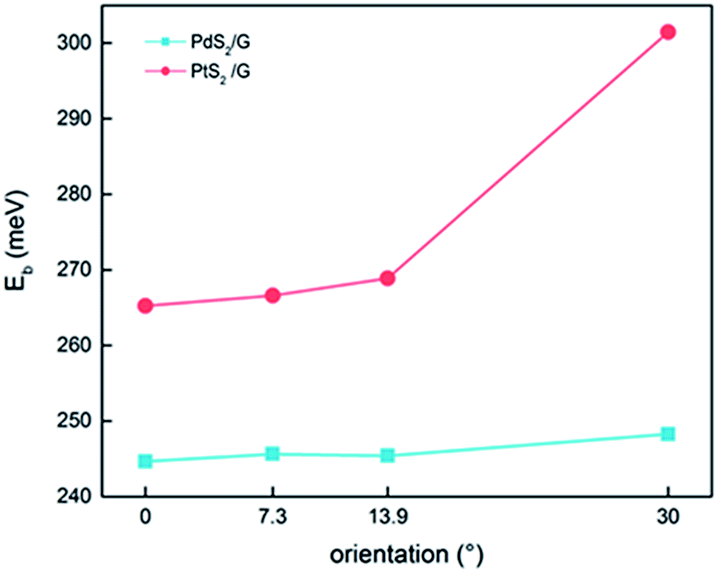 | ||
| Fig. 2 Variation of binding energy of stable PdS2/G (PtS2/G) heterojunctions with the interface angle. | ||
3.2 Electronic properties
The electronic properties of graphene-related heterostructures might be affected by interlayer rotations. To reveal this effect on MS2, the band structures of the heterostructures with different rotation angles have been calculated as shown in Fig. 3. The PtS2 and PdS2 band gaps in the heterostructures will be greater than the current PBE values in HSE, while the band structure of graphene will not change significantly.57 The spin orbital effect is not considered because no significant changes in the band gap or the band structure were observed in any of the monolayers of PtS2 and PdS2, and the band gap has no obvious change and the positions of the CBM and VBM do not move.17 To distinguish the contribution of each constituent layer more clearly, the energy states originated primarily from graphene are highlighted by red lines. All the Dirac points of graphene move to gamma points because the primitive cells of graphene used are multiples of . The free-standing PtS2 and PdS2 monolayers are semiconductors with bandgaps of 1.11 eV and 1.75 eV, respectively.17 When in contact with graphene, the band structure of PtS2 (PdS2) and graphene can be easily recognized, indicating the weak interlayer interaction. When the interlayer rotation angle is zero, the band gaps of PtS2 and PdS2 are 0.95 eV and 1.71 eV, respectively. The reduction of the bandgap of PtS2 (PdS2) after contact with the graphene layer is caused by the weak interlayer interactions. Remarkably, the Fermi level of the heterojunction moves to the position near the conduct band minimum (CBM) of MS2, indicating that MS2 is n-doped. The DFT calculations also show that MoS2 and WS2 have been slightly n-type doped in the MoS2/G and WS2/G heterostructures.51,52 In the experimentally fabricated MoS2 and WS2 transistors with graphene electrodes, such n-type transfer characteristics have also been observed.53,54 We believe this theoretical and experimental consistency with similar systems to our studied ones provides strong support for the reliability of our prediction. Now we can check the effect of different interlayer rotation angles. In both PtS2/G and PdS2/G heterostrucures, graphene always retains its semi-metallic character, and there is no band gap opened at its Dirac point, as the interlayer rotation angle changes. An obvious variation of the MS2 band structure is the positions of the valence band maximum (VBM) and conduct band minimum (CBM). When the interlayer angle is greater than 7 degrees, the CBM moves towards the K point in PdS2/G. For PtS2/G, the CBM and VBM all locate between the K and gamma points, except for the interlayer rotation angles, which are 13.9 degrees. As the rotation angle increases, the band gap of PdS2 is almost unchanged while that of PtS2 changes significantly from 1.71 eV to 1.56 eV when in contact with graphene.
 | ||
| Fig. 3 Band structure of the monolayers PdS2 (a–d) and PtS2 (e–h) on graphene with different interface angles. The red lines and blue lines represent the band structures of graphene and MS2, respectively. The Fermi level is set to zero and marked by dashed lines. | ||
Due to the quasi-metal nature of graphene, this kind of heterojunction can be regarded as a metal–semiconductor contact. For n-type semiconductors, electrons near the CBM are primarily responsible for electric conduction. At the metal–semiconductor interface, the electrons of lowest-lying states (located at the CBM) for an n-type semiconductor can spontaneously flow to the metal. The states will be offset when electronic transport occurs across the metal–semiconductor interface known as the n-type Schottky barrier height (SBH). The flow of electrons from the semiconductor to the metal is easier than conduction in the opposite direction. The SBH controls the transport of electrons crossing the metal–semiconductor interface. Because the current flow across the MS2 interface depends on the magnitude of the SBH, the SBH is clearly the most important property of a metal–semiconductor interface. The vertical Schottky barrier ΦV for the above case can be obtained from the energy difference between the Ef value of the interfacial system and the CBM (electron SBH) of the contacted MS2.
For MS2 in contact with graphene at an interlayer rotation angle of zero degrees, the vertical Schottky barrier is absent, which indicates that the heterojunction forms an ohmic contact. The Schottky barriers are n-type with ΦV = 0.035 eV, 0.021 eV, and 0.042 eV for PtS2/G at angles of 7.3°, 13.9° and 30°, respectively, and with ΦV = 0.017 eV, 0.015 eV and 0.057 eV for PtS2/G at angles of 7.3°, 13.9° and 30°, respectively. Since the values of the n-type SBH are all less than 0.06 eV in all cases, the MS2/G heterojunction can be regarded as a robust quasi-ohmic contact against the interlayer rotation angles.
3.3 Charge redistribution
To illustrate the nature of charge transference and Fermi level shift at the MS2-graphene interface, the charge density differences of non-twisted PdS2/G and PtS2/G are plotted in Fig. 4(a) and (b). Due to the difference in electronegativity between the sulfur and carbon atoms, an electrostatic potential difference between the two constituents will be established upon the adhesion of graphene on MS2, leading to a spontaneous polarization at the interface. The generated vertical electric field points from MS2 to graphene. Such charge transference from PtS2 (PdS2) to the graphene layer has been verified by further Bader charge analysis (Fig. 4(c)). Bader charge analysis can specifically describe the influence of the interlayer angle on the interlayer charge transference with a measurable value. The Y-axis Q is defined as the average electronic quantity gained by a single carbon atom, which is shown in the equation below:where n and N represent the order and total number of carbon atoms of the graphene monolayer in the MS2/graphene bilayer; QG and QC represent the electric quantity of a single carbon atom of the calculated system and the electric quantity of a pristine carbon atom, respectively.
 | ||
| Fig. 4 Plot of charge density differences of PdS2/G (a) and PtS2/G (b). The green and orange areas represent electron increase and decrease, respectively. The purple, cyan, yellow and gray spheres represent the Pd, Pt, S and C atoms, respectively. (c) Charge variation per C atom versus rotation angles in the MS2/G systems. | ||
In Fig. 4(c), the calculated Bader charge of the graphene layer is negative, which means that graphene loses electrons and MS2 is n-type doped. In our work, the relative difference of the Bader charge can quantitatively represent the charge redistribution around the interface. The results show that this charge transference is getting weaker as the rotation angle reaches 30 degrees. As the rotation angle increases, the number of electrons that the graphene layer gains becomes slightly less in both the PtS2 and PdS2 cases. This slight change in the number of transferred electrons might be related to the different local interfacial geometries in the heterostructures with different rotation angles.
3.4 Tunneling barrier
The tunneling barrier is an important figure of merit to evaluate the charge injection efficiency of an electrical contact. The tunneling barrier height ΦTB is defined as the potential energy above Ef between the non-twisted MS2 and graphene surfaces indicated by the red line in Fig. 5. The tunneling barrier heights ΦTB of the heterostructures with different rotation angles are listed in Table 1. The value of ΦTB elevates as the rotation angle increases in the PtS2/G systems, while this characteristic is completely opposite in the PdS2/G systems. The tunneling probabilities TB from graphene to MS2 are measured using a square potential barrier model such as:where m is the effective mass of a free electron, ωB is the width of the tunneling barrier (defined as the full width at half maximum of ΦTB), and ℏ is the reduced Planck constant. The value of TB is computed by this equation to be 13.0 (10.0), 16.5 (9.7), 16.5 (13.9), and 22.1 (11.4) % as the rotation angle increases from 0° to 7.3°, 13.9° and 30° for PdS2/G (PtS2/G), respectively. These tunneling probabilities are not high compared with the nearly 100% value in some bulk metal contacted systems such as Ni contacted phosphorene55 and Ti contacted MoS2.56 Interfacial strong covalent bonds are usually formed in these electrical contacts with high tunneling probabilities. The relatively low tunneling probability in the PtS2/G and PdS2/G heterostructures comes from the weak interlayer interaction.
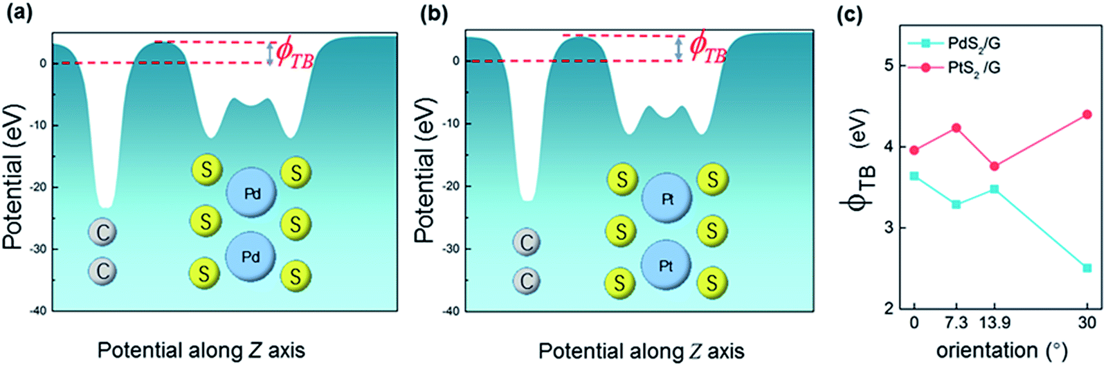 | ||
| Fig. 5 Plot of electric potential versus z potential for PdS2/G (a) and PtS2/G (b). (c) Tunneling barrier of two types of heterojunctions as a function of rotation angle. | ||
4. Conclusions
In conclusion, the structure and electronic properties of PtS2/G and PdS2/G heterojunctions with different interlayer rotation angles are studied by DFT calculations. The structure and electronic properties of MS2/G heterojunctions are almost robust under stacking. The two layers are combined by weak van der Waals interactions, and the heterojunction becomes more stable as the AC direction of graphene coincides with the ZZ direction of MS2. A slight charge transference from graphene to PtS2 (PdS2) occurs, resulting in a vertical build-in internal electric field and PtS2 (PdS2) being n-doped. Schottky barriers change in a small range from 0 eV to 0.057 eV in both heterobilayers with different orientations between the two monolayers. In terms of the robust quasi-ohmic nature against the interlayer rotation angle, MS2/G heterobilayers are potential electrical contacts for high performance nano-electronic devices.Conflicts of interest
There are no conflicts to declare.Acknowledgements
This work was supported by the National Natural Science Foundation (No. 61675032, 61671085, and 11604019), the National Basic Research Program of China (973 Program) under Grant No. 2014CB643900, the Open Program of the State Key Laboratory of Functional Materials for Informatics, the National Natural Science Foundation for Theoretical Physics special fund “cooperation program” (No. 11547039), and the Shaanxi Institute of Scientific Research Plan projects (No. SLGKYQD2-05).References
- K. S. Novoselov, A. K. Geim and S. V. Morozov, Science, 2004, 306, 666–669 CrossRef CAS PubMed.
- A. K. Geim and K. S. Novoselov, Nat. Mater., 2009, 6, 183–191 CrossRef PubMed.
- S. Zhang, J. Zhou and Q. Wang, Proc. Natl. Acad. Sci. U. S. A., 2015, 112(8), 2372–2377 CrossRef CAS PubMed.
- F. Q. Wang, J. Yu and Q. Wang, Carbon, 2016, 105, 424–429 CrossRef CAS.
- P. Miro, M. Audiffred and T. Heine, Chem. Soc. Rev., 2014, 43, 6537–6554 RSC.
- T. Heine, Acc. Chem. Res., 2015, 48(1), 65–72 CrossRef CAS PubMed.
- H. I. Karunadasa, E. Montalvo and Y. Sun, Science, 2012, 335, 698–702 CrossRef CAS PubMed.
- C. Zhu, X. Mu and P. A. van Aken, Angew. Chem., Int. Ed., 2014, 53, 2152–2156 CrossRef CAS PubMed.
- E. Gourmelon, O. Lignier and H. Hadouda, Sol. Energy Mater. Sol. Cells, 1997, 46, 115–121 CrossRef CAS.
- B. Hinnemann, P. G. Moses and J. Bonde, J. Am. Chem. Soc., 2005, 127(15), 5308–5309 CrossRef CAS PubMed.
- G. Zhang, H. J. Liu, J. H. Qua and J. H. Li, Energy Environ. Sci., 2012, 9(4), 1190–1209 Search PubMed.
- K. F. Mak, C. Lee, J. Hone, J. Shan and T. F. Heinz, Phys. Rev. Lett., 2010, 105, 136805 CrossRef PubMed.
- B. Radisavljevic, A. Radenovic, J. Brivio, V. Giacometti and A. Kis, Nat. Nanotechnol., 2011, 6(3), 147–150 CrossRef CAS PubMed.
- F. Grønvold and E. Rost, Acta Chem. Scand., 1956, 10, 1620–1634 CrossRef.
- A. Kjekshus and F. Grønvold, Acta Chem. Scand., 1959, 13, 1767 CrossRef CAS.
- F. Grønvold, H. Haraldsen, A. Kjekshus and R. Söderquist, Acta Chem. Scand., 1960, 14, 1879–1893 CrossRef.
- P. Miro, M. Ghorbani-Asl and T. Heine, Angew. Chem., Int. Ed., 2014, 53, 3015–3018 CrossRef CAS PubMed.
- Y. D. Zhao, J. S. Qiao, P. Yu, Z. X. Hu, Z. Y. Lin, S. P. Lau, Z. Liu, W. Ji and Y. Chai, Adv. Mater., 2016, 28, 2399–2407 CrossRef CAS PubMed.
- W. X. Zhang, Z. S. Huang, W. L. Zhang and Y. R. Li, Nano Res., 2014, 7(12), 1731–1737 CrossRef CAS.
- K. S. Novoselov, A. Mishchenko, A. Carvalho and A. H. Castro Neto, Science, 2016, 353(6298), 1–25 CrossRef PubMed.
- Y. Cai, C. P. Chu, C. M. Wei and M. Y. Chou, Phys. Rev. B: Condens. Matter Mater. Phys., 2013, 88(24), 245408 CrossRef.
- B. Liu, J. A. Baimova, C. D. Reddy, S. V. Dmitriev, W. K. Law, X. Q. Feng and K. Zhou, Carbon, 2014, 79, 236–244 CrossRef CAS.
- W. Yang, G. Chen and Z. Shi, et al., Nat. Mater., 2013, 12(9), 792 CrossRef CAS PubMed.
- K. Roy, M. Padmanabhan, S. Goswami, T. P. Sai, G. Ramalingam, S. Raghavan and A. Ghosh, Nat. Nanotechnol., 2013, 8(11), 826–830 CrossRef CAS PubMed.
- W. Zhang, C. P. Chuu and J. K. Huang, et al., Sci. Rep., 2014, 4(7484), 3826 Search PubMed.
- J. E. Padilha, A. Fazzio and A. J. da Silva, Phys. Rev. Lett., 2015, 114(6), 066803 CrossRef CAS PubMed.
- G. Giovannetti, P. A. Khomyakov, G. Brocks, P. J. Kelly and J. van den Brink, Phys. Rev. B: Condens. Matter Mater. Phys., 2007, 76, 073103 CrossRef.
- L. Britnell and L. A. Ponomarenko, Science, 2011, 335, 947 CrossRef PubMed.
- G. H. Lee, Y. J. Yu and X. Cui, et al., ACS Nano, 2013, 7(9), 7931–7936 CrossRef CAS PubMed.
- S. Sattar and U. Schwingenschlögl, ACS Appl. Mater. Interfaces, 2017, 9(18), 15809–15813 CAS.
- J. Pu, Y. Yomogida, K. K. Liu, L. J. Li, Y. Iwasa and T. Takenobu, Nano Lett., 2012, 2(8), 4013–4017 CrossRef PubMed.
- W. J. Yu, Z. Li, H. L. Zhou, Y. Chen, W. Yang, Y. Huang and X. F. Duan, Nat. Mater., 2013, 12(3), 246–252 CrossRef CAS PubMed.
- H. Tian, Z. Tan and C. Wu, et al., Sci. Rep., 2014, 4, 5951 CrossRef CAS PubMed.
- Y. Murata, E. Starodub, B. B. Kappes, C. V. Ciobanu, N. C. Bartelt, K. F. McCarty and S. Kodambaka, Appl. Phys. Lett., 2010, 97(14), 14–16 CrossRef.
- B. B. Kappes, A. Ebnonnasir, S. Kodambaka and C. V. Ciobanu, Appl. Phys. Lett., 2013, 102(5), 5–10 CrossRef.
- Y. Murata, S. Nie, A. Ebnonnasir, E. Starodub, B. B. Kappes, K. F. McCarty, C. V. Ciobanu and S. Kodambaka, Phys. Rev. B: Condens. Matter Mater. Phys., 2012, 85(20), 205443 CrossRef.
- Z. Ni, L. Liu, Y. Wang, Z. Zheng, L. J. Li, T. Yu and Z. Shen, Phys. Rev. B: Condens. Matter Mater. Phys., 2009, 80, 125404 CrossRef.
- J. M. B. Lopes dos Santos, N. M. R. Peres and A. H. Castro Neto, Phys. Rev. Lett., 2007, 99, 256802 CrossRef CAS PubMed.
- Y. Wang, Z. Ni, L. Liu, Y. Liu, C. Cong, T. Yu, X. Wang, D. Shen and Z. Shen, ACS Nano, 2010, 4, 4074–4080 CrossRef CAS PubMed.
- J. M. B. Lopes dos Santos, N. M. R. Peres and A. H. Castro Neto, Phys. Rev. B: Condens. Matter Mater. Phys., 2012, 86, 155449 CrossRef.
- Z. Wang, Q. Chen and J. Wang, J. Phys. Chem. C, 2015, 119(9), 4752–4758 CAS.
- W. Kohn and L. J. Sham, Phys. Rev., 1965, 140(4A), A1133–A1138 CrossRef.
- G. Kresse and J. Furthmüller, Comput. Mater. Sci., 1996, 6(1), 15–50 CrossRef CAS.
- P. E. Blöchl, Phys. Rev. B: Condens. Matter Mater. Phys., 1994, 50(24), 17953 CrossRef.
- G. Kresse and G. Joubert, Phys. Rev. B: Condens. Matter Mater. Phys., 1999, 59(3), 1758 CrossRef CAS.
- D. M. Ceperley and B. J. Alder, Phys. Rev. Lett., 1980, 45(7), 566 CrossRef CAS.
- J. P. Perdew, K. Burke and M. Ernzerhof, Phys. Rev. Lett., 1996, 77(18), 3865 CrossRef CAS PubMed.
- S. Grimme, J. Comput. Chem., 2006, 27(15), 1787–1799 CrossRef CAS PubMed.
- H. J. Monkhorst and J. D. Pack, Phys. Rev. B: Solid State, 1976, 13(12), 5188 CrossRef.
- A. Kolmogorov and V. Crespi, Phys. Rev. B: Condens. Matter Mater. Phys., 2005, 71, 235415 CrossRef.
- B. Heldt, Nanoscale, 2011, 3(9), 3883 RSC.
- F. Zhang, W. Li, Y. Ma, Y. Tang and X. Dai, RSC Adv., 2017, 7(47), 29350–29356 RSC.
- L. Yu, Y. H. Lee and X. Ling, et al., Nano Lett., 2014, 14(6), 3055 CrossRef CAS PubMed.
- W. Zhang, J. K. Huang and C. H. Chen, et al., Adv. Mater., 2013, 25(25), 3456 CrossRef CAS PubMed.
- Y. Pan, Y. Wang and M. Ye, et al., Chem. Mater., 2016, 28(7), 2100–2109 CrossRef CAS.
- H. Zhong, R. Quhe and Y. Wang, et al., Sci. Rep., 2016, 6, 21786 CrossRef CAS PubMed.
- J. Gusakov, B. K. Tay and V. Gusakov, Phys. Status Solidi A, 2016, 213(11), 2834–2837 CrossRef.
| This journal is © The Royal Society of Chemistry 2017 |