
 Open Access Article
 This Open Access Article is licensed under a
 Creative Commons Attribution 3.0 Unported Licence
A sensitive DNA sensor based on an organic electrochemical transistor using a peptide nucleic acid-modified nanoporous gold gate electrode†
Wenyan Tao abc,
Peng Lin*a,
Jin Hua,
Shanming Kea,
Jiajun Songa and
Xierong Zenga
abc,
Peng Lin*a,
Jin Hua,
Shanming Kea,
Jiajun Songa and
Xierong Zenga
aShenzhen Key Laboratory of Special Functional Materials, Shenzhen Engineering Laboratory for Advance Technology of Ceramics, College of Materials Science and Engineering, Shenzhen University, Shenzhen, China. E-mail: lin.peng@szu.edu.cn; Fax: +86 755 26536239; Tel: +86 755 26537459
bKey Laboratory of Optoelectronic Devices and Systems of Ministry of Education, College of Optoelectronic Engineering, Shenzhen University, Shenzhen, Guangdong Province, China
cDepartment of Electronic Engineering, The Chinese University of Hong Kong, Shatin, Hong Kong
First published on 9th November 2017
Abstract
An organic electrochemical transistor (OECT) based on poly(3,4-ethylenedioxythiophene):polystyrene sulfonate with porous anodic aluminum oxide (AAO) as a gate electrode was proposed for DNA sensing. The AAO substrate, which possesses a pore size of 200 nm, underwent gold nanofilm deposition by the thermal evaporation technique and is referred to as a nanoporous gold electrode in this work. Due to its high sensitivity, target DNA as low as 0.1 nM in concentration was achieved on an OECT device with a nanoporous gold gate electrode using a peptide nucleic acid probe. One-base and two-base mismatched DNA sequences could be discriminated. A sensing mechanism for the OECT device based on the nanoporous gold electrode was proposed. The synergetic effect of capacitance with the surface potential on the nanoporous gold electrode enlarged the increase in gate potential, which resulted in high sensitivity for DNA sensing.
1. Introduction
An organic thin-film transistor (OTFT)-based sensor normally possesses high sensitivity because the device is the combination of a sensor and an amplifier, in which a small change of the effective gate voltage induced by the analyte may lead to a pronounced variation of channel current. Therefore, sensors based on transistors have many advantages, including low cost, easy fabrication, and high throughput sensing. Such sensors have emerged as an ultrasensitive platform for detecting charged biomolecules such as protein and DNA.1–3 For example, Khan et al. fabricated an OTFT sensor based on 5,5-bis-(7-dodecyl-9H-fluorene-2-yl)-2,2′-bithiophene (DDFTTF) as the active layer, which can be used for in situ detection of the hybridization of DNA at concentrations as low as 1 nM.2 Thus, OTFT-based sensors are usable and highly sensitive.One type of OTFT is the organic electrochemical transistor (OECT), which has recently gained much attention because it can be used in aqueous solutions with stable performance at low operating voltages (approximately 1 V). For example, a poly(3,4-ethylene dioxythiophene) (PEDOT: PSS)-based OECT has been used for dopamine,4 glucose,5 and DNA sensing.6 Furthermore, it has been integrated into a microfluidic system for multi-analyte analysis.7 The fabrication of an OECT is easy and flexible because the gate electrode and the channel of the device are separated. Therefore, the gate electrode can be fabricated from different nanomaterials as compared to those used for the source and drain electrodes. Due to their highly specific surface, nanostructured materials would be considered as gate electrode materials in this work. Normally, nanostructured materials are composed of nanoparticles of various sizes, nanorods, nanowires of various diameters and lengths, and gratings of various shapes, supported on either dielectric or conducting substrates. Through employing a nanostructured template, a metal nanoparticle film can easily be formed.
Peptide nucleic acid (PNA) probes offer significant advantages over DNA probes in DNA sensing because of their higher sensitivity and specificity. The molecular structure of PNA molecules consists of a sugar-phosphate backbone that has been replaced with a peptide-like N-(2-aminoethyl)glycine polyamide structure, to which the nucleobases are connected by methylene carbonyl linkages. PNA has gained much attention because of its favorable properties.8–12 PNA probes possess two main advantages over DNA probes in an OECT device: first, PNA produces ultra-small background noise because PNA is neutral; second, PNA can increase the hybridization rate and efficiency. The neutral backbone of PNA results in the formation of a less dense charge layer, which allows PNA/DNA hybridization to occur at low ionic strength favored by the OECT response. The neutral backbone of PNA also allows hybridization with DNA at a faster rate and with a greater affinity than a DNA probe. Additionally, a higher thermal stability of PNA/DNA duplexes is observed, with temperature largely independent of salt concentration in the hybridization solution.13
The DNA hybridization process is significant to chip-based characterization of gene expression patterns and detection of pathogens. Current optical assays are based on the hybridization of a labeled DNA target strand to a complementary or mutated capture strand.14–16 In order to obtain sufficient sensitivity and advance the optical output, the polymerase chain reaction has been integrated into optical sensors to amplify the target DNA,17 which is tedious and time-consuming. Furthermore, a few studies have reported DNA hybridization using a PNA probe on a silicon-oxide nanowire transistor,18 Si-nanograting transistor,19 and graphene transistor.20 After the PNA probe hybridized with the DNA target, an accumulation of negative charges on the sensing surface resulting from the negatively charged DNA backbone would cause a conductance change in the transistor. Although these sensors exhibited an extremely low detection limit of 10 fM for target DNA, micro electromechanical system (MEMS) techniques of e-beam lithography and plasma etching would be necessary for the fabrication of this device, and these methods are complicated and costly. Therefore, it is critical to seek a low-cost device with high sensitivity and easy fabrication for DNA sensing. Additionally, single nucleotide polymorphisms, a common form of genetic variations in the human genome, are important to disease diagnosis and detection of disease predisposition.21,22 Therefore, the detection of a single- or two-base mismatch has been given much consideration by electrochemical,23,24 optical,25 and other methods.26 However, designing highly sensitive and selective probes for a single- or two-base mismatch is not easy, and the fabrication process is complex.
In this work, highly ordered and porous anodic aluminum oxide (AAO) with a nanopore size of 200 nm was employed as the template. Gold nanofilm was conveniently fabricated on an AAO template by the thermal evaporation technique. The thus formed nanoporous gold electrode was used as a gate electrode in the OECT device. The PNA probe was adapted for DNA sensing due to its higher sensitivity and specificity. The sensing mechanisms were attributed to the modulation of surface potential of the gate electrode induced by the PNA-DNA hybridization process, which eventually caused a change in the source-drain current. DNA chains with different mismatched bases were also discriminated on this type of OECT device.
2. Experimental
2.1 Material
DNA strands were purchased from Sangon Biotech Co. Ltd. (Shanghai, China); the sequences are listed in Table 1. The PNA probe was ordered from ZIYU Biotech Co. Ltd. (Shanghai). The highlighted DNA represents the location of non-complementary base pairs with respect to the probe sequence. Tris–HCl buffer was used to store and transport DNA (50 mM, pH 7.0), and phosphate-buffered saline (PBS, 10 mM, pH 7.0) was used as an aqueous electrolyte for testing. Mercaptohexanol (MCH) was of analytical grade. Porous alumina membrane with an average pore size of 200 nm was purchased from Whatman (Whatman International Ltd.). Water used for sample preparation was deionized with a Thermo Micro-Pure water purification system to resistivity of 18.2 MΩ cm.| Name | Sequences |
|---|---|
| PNA probe | Cys–OO–-OO-ATCCATCTCC-CONH2 |
| Complementary DNA target (cDNA) | 5′’- TAGGTAGAGG -3′’ |
| Random DNA target | 5′’- ATTTCCCGTC -3′’ |
| One-base mismatched DNA | 5′’- TAGGCAGAGG -3′’ |
| Two-base mismatched DNA | 5′’- TAGCTACAGG -3′’ |
| Three-base mismatched DNA | 5′’- TCGGAAGCGG -3′’ |
| Cys–OO–OO– | 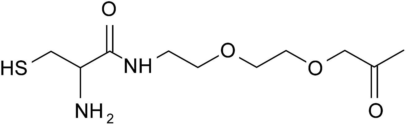 |
2.2 Device fabrication
Glass slides were used as substrates for fabrication of OECT devices. Gold electrodes for the source-drain were deposited by thermal evaporation through a shadow mask. The width and length of the channel are 200 μm and 6 mm, respectively. The process flow for source-drain electrode fabrication is shown in the ESI, Fig. S1.† Prior to the coating of the PEDOT: PSS layer, the glass slides were treated with oxygen plasma for 5 min to improve the film adhesion. Then, the PEDOT: PSS solution was spin-coated at 3500 rpm onto the patterned substrates, and the samples were annealed at 200 °C for 60 min in a glove box filled with high purity N2 gas. The thickness of the PEDOT: PSS film was approximately 80 nm.The gate electrode was prepared by thermal evaporation of a gold film on a highly ordered AAO membrane with a pore diameter of approximately 200 nm. The circular-shaped AAO membranes were all of a diameter of 13 mm with a thickness of 60 μm. Before metal deposition, the substrates were rinsed with ethanol and ultrapure water alternatively three times, dried in ambient air, and then fixed on a silicon plate. The gold film was then fabricated by the Nexdep Thin Film 400 deposition system in a base vacuum of approximately 1 × 10⁻⁷ Torr. The deposition rate was set at 0.1 Å s−1. The thus formed gold nanofilm is called a nanoporous gold electrode in this work. The process flow for gate electrode fabrication is shown in the ESI, in Fig. S2.† Morphological characterization was obtained using a JSF-6700 (JEOL) field emission scanning electron microscope at operation potential of 5 kV.
2.3 Immobilization of the PNA probe
The immobilization of the PNA probe on the nanoporous gold electrode is as follows: firstly, the electrode was immersed in a 10 μM PNA solution for 12 h, followed by rinsing with PBS and water three times to remove nonspecifically absorbed PNA molecules. Finally, the electrode was further treated with 1 mM MCH solution prepared in ethanol/ultrapure water for 2 h to block unoccupied sites.2.4 Measurements
As shown in Scheme 1 for the setup, the DNA sensing experiments were performed by detecting the change in the channel current of the OECT before and after PNA-DNA hybridization. The current was measured between two terminals, the source (S) and drain (D) electrodes, with a Keithley 4200-SCS Source Measure Unit connected to the gate electrode.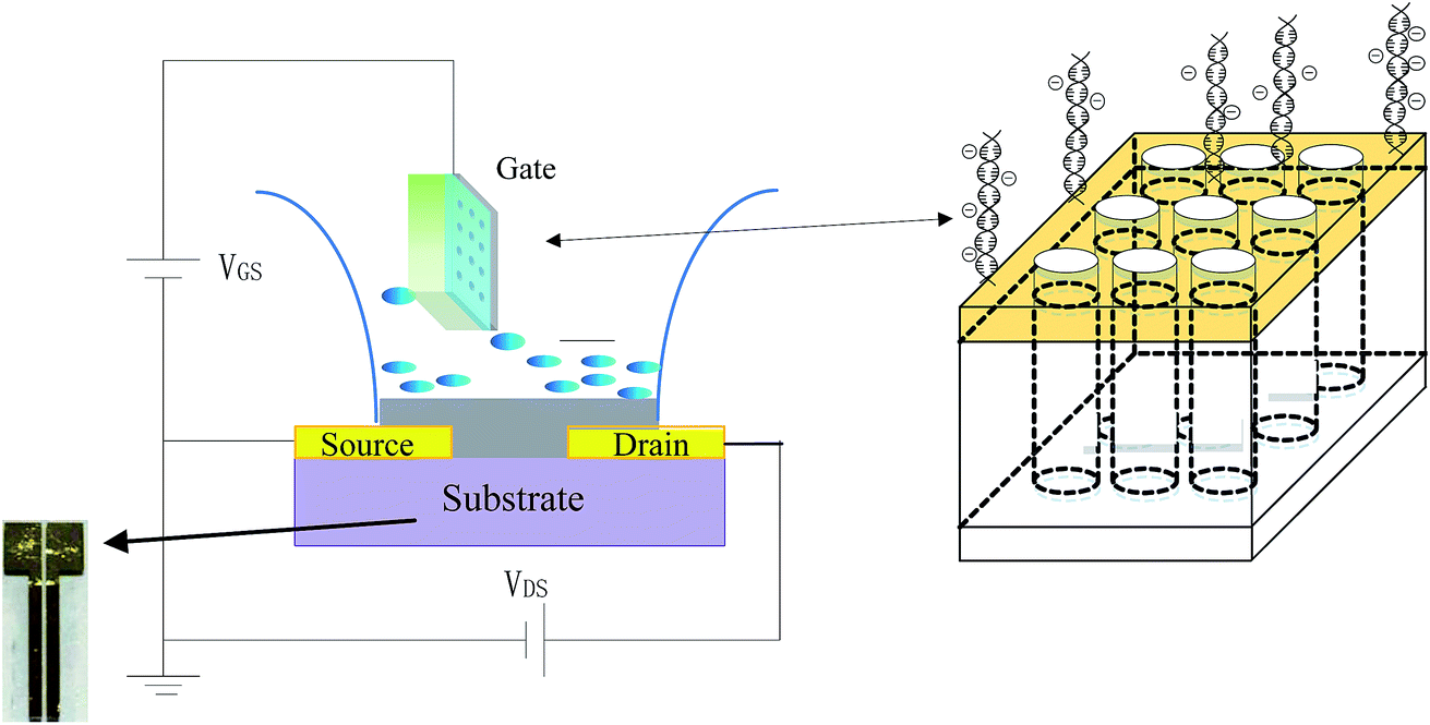 | ||
| Scheme 1 Schematic illustrations of the nanoporous gold gate electrode-based OECT device for DNA sensing. The colors in the figure indicate the following: purple: glass substrate; yellow-source and yellow-drain: a gold layer with thickness of 100 nm; the width and length of the channel between the source and drain is 200 μm and 6 mm, respectively; Grey: PEDOT: PSS layer with thickness of 80 nm; blue droplet: PBS buffer solution; green square: nanoporous gold electrode, whose structure is shown in the right square shape with the cylinder array. | ||
To maximize the hybridization efficiency and OECT response, the hybridization proceeded for 90 min prior to acquiring signal in this experiment. Different OECT devices were used for each individual measurement. At least three OECT devices were measured each time, and the mean value of the current was utilized for data analysis. All measurements were carried out at room temperature (25 ± 2 °C).
3. Results and discussion
3.1 Data analysis
As demonstrated in Fig. 1, gold nanoparticles and holes are regularly linked with each other in the nanoporous gold electrode. Several structural features emerge from the micrographs. First, gold film was deposited on AAO substrates mainly by surrounding the nanopores. Second, the gold film mainly consists of nanoparticles in good homogeneity. It suggests that the deposited gold nanoparticles are in good crystalline structure, similar with that in the previous work.27 Therefore, gold nanoparticles link with each other along the AAO substrate frames to form a compact structure. The peculiar structure suggests that electric properties of the as-fabricated nanoporous gold electrode would be affected not only by that of individual particles but also by their linear and ring-shaped aggregates. They allow the electrode to possess a larger active electrochemical area and higher conductivity, which facilitate the electron transfer rate of the nanoporous gold gate electrode and result in higher sensitivity of the OECT device. At the same time, the “nanocavities” observed in the nanoporous gold electrode are actually the 2-dimensional enclosures formed by linked nanoparticles and are different from the conventional arrays of “nanocavities” formed on a homogeneous metal film.28,29 Additionally, the stereo structure of “nanocavities” on a nanoporous gold electrode results in PNA that possesses higher bioactivity after immobilization, which facilitates PNA-DNA hybridization.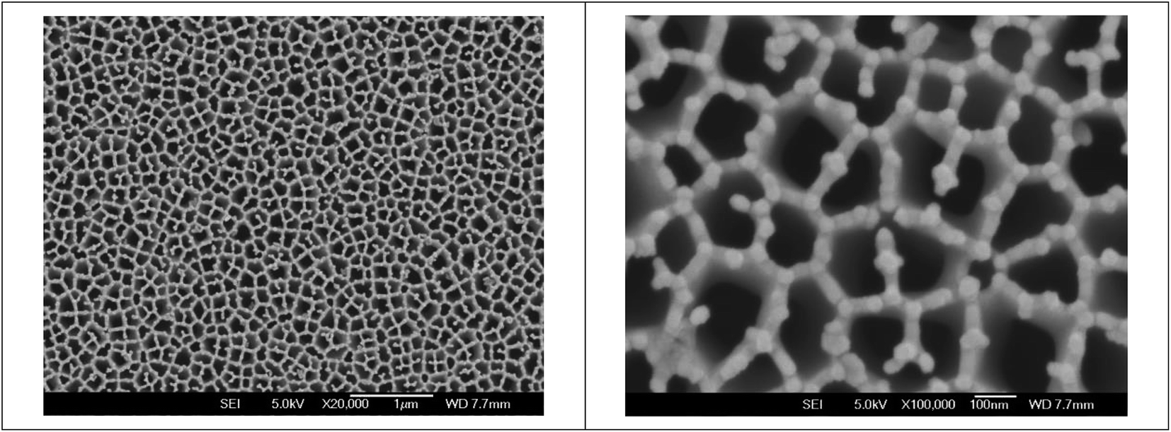 | ||
Fig. 1 Field-emission SEM images of a nanoporous gold gate electrode. The scale bars are 1 μm and 100 nm for the magnifications of 20![[thin space (1/6-em)]](https://www.rsc.org/images/entities/char_2009.gif) 000× and 100000× , respectively. 000× and 100000× , respectively. | ||
Fig. 2 shows the transfer characteristics of an OECT device with an immobilization PNA probe and the hybridization of complementary DNA (cDNA). After hybridization with cDNA, it can be found that the transfer curve horizontally shifts to a higher gate voltage of 16 mV for 0.5 nM cDNA and 60 mV for 5 nM cDNA, respectively. The PBS buffer background response is approximately 2 mV, and therefore, the response value for cDNA could be used as sensing signal.
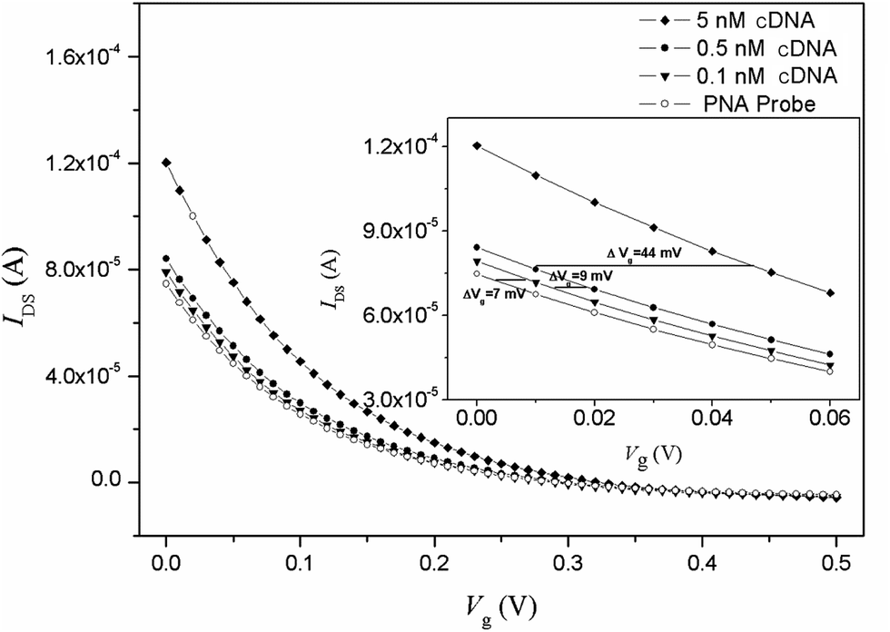 | ||
| Fig. 2 Transfer characteristic curves of the OECT based on the nanoporous gold gate electrode in 10 mM PBS containing different concentrations of cDNA target. The inset shows the horizontal shifts of the transfer curves. VDS =−0.1 V. | ||
Additionally, the real-time kinetics of DNA hybridization on an OECT device was investigated by its transfer curve response. It was found that the PNA-DNA hybridization to the OECT device reached equilibrium at approximately 90 min (see the ESI, Fig. S3†).
To verify the PNA/DNA hybridization equilibration time, an EIS technique was selected for on-line monitoring of the PNA/DNA hybridization process on a nanoporous gold electrode. Additionally, a suitable equivalent circuit model was adopted for EIS data fitting (see the ESI, Fig. S4 and S5†). Because PNA is neutral and DNA possesses some negative charges, the electrode surface turned from neutral to negative after hybridization. Obviously, the electron-transfer resistance (Rct), which is correlated to the diameter of the Nyquist plot semicircle, gradually increased with increasing hybridization time. It is consistent with the electrostatic repulsion of Fe(CN)63−/4− from the electrode interface by formation of a negatively charged PNA/DNA duplex, thereby introducing a barrier for interfacial electron transfer. Rct reached a plateau value after 90 minutes, indicating that the PNA/DNA hybridization reaction reached equilibrium. The fitting data are listed in Table 2. It was found that the gate capacitance (Cg) for the nanoporous gold electrode before and after the DNA hybridization was 28.3 μF cm−2 and 14.6 μF cm−2, respectively.
| Parameter | PNA-modified | PNA/DNA-modified |
|---|---|---|
| Rs (Ω cm2) | 8.03 | 6.04 |
| Cdl (F cm−2) | 2.83 × 10⁻⁵ | 1.46 × 10⁻⁵ |
| Rct (Ω cm2) | 86.51 | 108.45 |
| Q1 − Y0 (F cm−2) | 5.03 × 10⁻⁴ | 2.46 × 10⁻⁴ |
| Q1 − n | 0.90 | 0.98 |
| Rx1 (Ω cm2) | 110.86 | 183.47 |
| Q2 − Y0 (F cm−2) | 1.76 × 10⁻⁴ | 2.07 × 10⁻⁴ |
| Q2 − n | 0.74 | 0.80 |
| Rx2 (Ω cm2) | 5.86 | 7.20 |
The selectivity was measured by varying the base pairs of mismatched DNA sequence in solution. The number of mismatched base pairs was increased until the signal decreased to that of a random sequence. A measurable difference in gate potential for a sequence with a one-base mismatch and two-base mismatch pair is observed in Fig. 3. However, that for a three-base mismatch DNA sequence exhibits responses indistinguishable from a fully random sequence.
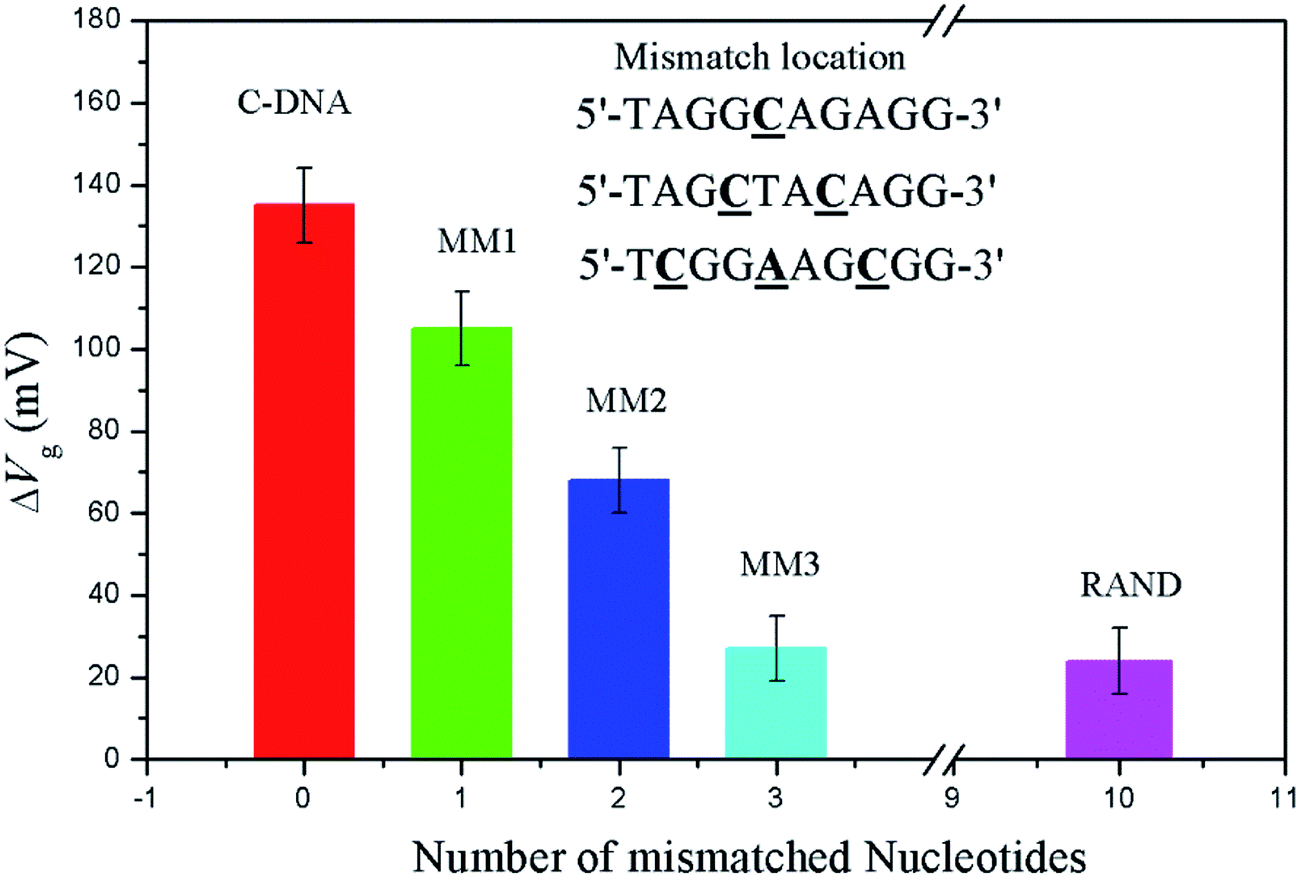 | ||
| Fig. 3 Response of the OECT based on the nanoporous gold gate electrode to complementary, mismatched, and random DNA targets. The error bars show the standard deviation of ≥3 devices. IDS = 7.47 × 10⁻⁵ A. | ||
The sensitivity was demonstrated by varying the concentration of target cDNA from 0.1 nM to 50 nM. The same hybridization process was conducted for a random DNA chain with a concentration of 1 μM, and the data were used as a negative control. Fig. 4 shows that the response of the sensor is saturated at high concentrations (>15 nM) but steadily declines for lower concentrations. The intrinsic background results from the shifting potentials of the gate electrode.30 The linear range for cDNA is from 0.5 nM to 12.5 nM. The linear equation is: ΔVg (mV) = 9.3CcDNA (nM) + 21.5 (r = 0.991). The limit of detection for the system is 0.1 ± 0.08 nM, assuming a signal-to-noise ratio of 3:1 with a background signal level of 2 mV resulting from the phosphate buffer solution. The limit of detection value is slightly better than that in a previous report describing an OECT device (1 nM) when no electric pulse was applied to the gate electrode.31
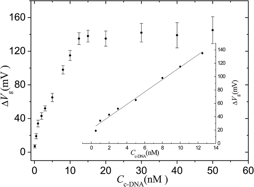 | ||
| Fig. 4 Response of the OECT based on the nanoporous gold gate electrode to different concentrations of cDNA target. The inset is the fitting curve for linear range. IDS = 7.47 × 10⁻⁵ A. | ||
3.2 Sensing mechanism
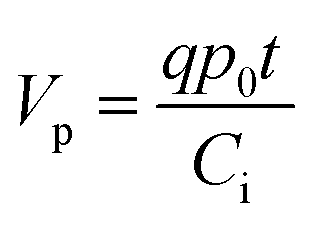
There are two important interfaces in the OECT device: the gate/electrolyte and the channel (PEDOT: PSS)/electrolyte interfaces. Each interface has an electric double layer (EDL), and Cg and Cc are the gate and channel capacitance, respectively. Because Cg and Cc are connected in series, the gate voltage (Vg) is distributed at the two interfaces. Additionally, the potential drop at the channel/electrolyte interface plays an important role in the modulation of the channel current of an OECT device. The channel current (IDS) of an OECT is given by the following equations:32,33
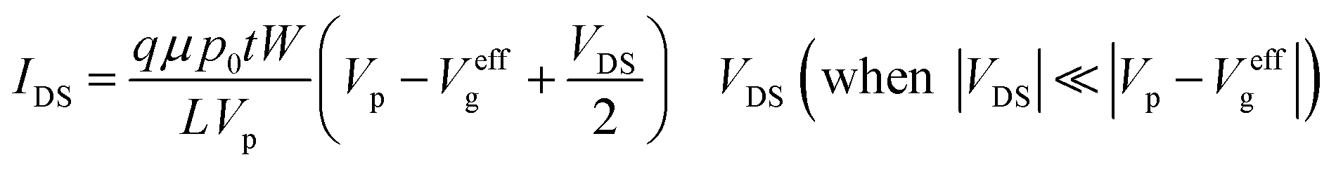 | (1) |
 | (2) |
| Veffg = Vg + Voffset | (3) |
ci is the effective capacitance per unit area of the transistor, which is related to not only the capacitance of the interface between the electrolyte and source-drain electrode (channel capacitance, Cc), but also the capacitance of the interface between the electrolyte and gate electrode (gate capacitance, Cg). Therefore, ci can be defined by the total capacitance of the two interfacial capacitors connected in series divided by the area of active layers (S), which is shown in the following equation:
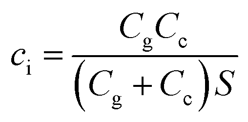 | (4) |
The capacitance Cc of the interface between the electrolyte and PEDOT: PSS has been found to be stable in the low voltage range (below 1 V).34 It was also found that the Cg values for the nanoporous gold gate electrode before and after DNA hybridization are 28.3 μF cm−2 and 14.6 μF cm−2, respectively (seen in Table 2).
The offset voltage is related to the potential drop at the two interfaces: gate/electrolyte and PEDOT: PSS/electrolyte. Because both the immobilization of the PNA probe and DNA hybridization occurred on the gate electrode, the potential change (ΔΨ) at the gate electrode surface is the only effect factor. Therefore,
| ΔVoffset = ΔΨ | (5) |
The surface potential change (ΔΨ) is effected by the surface dipole formed by the intrinsic charge of the DNA given by:
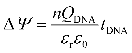 | (6) |
A detailed mechanism is explained in Scheme 2. After the DNA hybridization, additional negative charge (QDNA) of the complementary DNA is introduced onto the gate electrode surface. Partial gate potential would be used to offset the negative charge of the DNA, which results in a decrease in the effective gate voltage, as shown in state (1) in Scheme 2. To maintain the same effective gate voltage (Veffg) as that of the OECT device before the DNA hybridization, the applied gate voltage (Vg) needs to be increased after the hybridization of DNA. As a result, the transfer curve shifts positively to a higher gate voltage. Thus, the sensing mechanism is based on the modulation of surface potential induced by the hybridization of DNA molecules on the nanoporous gold gate electrode surface.
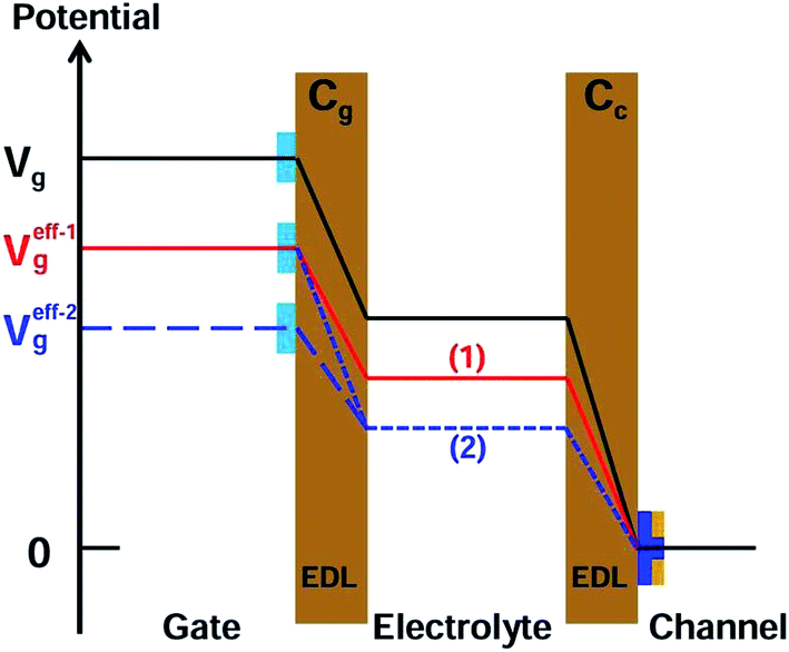 | ||
| Scheme 2 Schematic diagram for potential drops in the two double layers (EDL, shaded area), including channel/electrolyte and electrolyte/nanoporous gold gate, of an OECT before and after the modification and the hybridization of DNA on the gate electrode. | ||
According to eqn (1), (2), and (4), the effect of gate capacitance on the nanoporous gold gate electrode should be considered. From the EIS data (see the ESI, Fig. S3†), it can be found that Cg decreased after the DNA hybridization. Because Cg and Cc are connected in series and the potential drop at the gate/electrolyte interface would increase, the potential drop at the electrolyte/channel interface would decrease. It can be considered that the effective gate voltage would decrease further at this moment, as shown in state (2) in Scheme 2. As a result, the transfer curve would shift toward a more positive gate voltage. Therefore, the synergetic effect of gate capacitance with the surface potential of the nanoporous gold gate electrode will enlarge the increase in Vg, resulting in higher sensitivity for DNA sensing.
3.3 Repeatability and reproducibility
To investigate the repeatability of the OECT device based on the nanopore gold electrode, the potential shift response to 5 nM cDNA at five devices prepared in the same manner was recorded. The result is shown in Table 3. The relative standard deviation (R.S.D.) was 4.96%. At the same time, the reproducibility of the OECT device for cDNA sensing was investigated by having different people in our laboratory operate the same device, and the result is shown in Table 4. The R.S.D is 4.85%, which indicates that the reproducibility of the OECT device is good and acceptable for a DNA sensor.| Device no. | ΔVg (mV) | Mean values | R.S.D. |
|---|---|---|---|
| a ΔVg: the potential shift response of the PNA-modified OECT device hybridized with 5 nM cDNA. R.S.D.: relative standard deviation (n = 5). | |||
| 1 | 65 | ||
| 2 | 73 | ||
| 3 | 65 | 69 ± 3.40 | 4.93% |
| 4 | 67 | ||
| 5 | 73 | ||
| Person no. | ΔVg (mV) | Mean values | R.S.D. |
|---|---|---|---|
| a ΔVg: the potential shift response of the PNA-modified OECT device hybridized with 5 nM cDNA. R.S.D.: relative standard deviation (n = 5). | |||
| 1 | 66 | ||
| 2 | 68 | ||
| 3 | 71 | 71 ± 3.43 | 4.83% |
| 4 | 74 | ||
| 5 | 75 | ||
4. Conclusion
In this work, an OECT device based on porous anodic aluminum oxide-gold as the gate electrode was applied to DNA sensing for the first time. Due to the higher specificity of the PNA probe and the higher sensitivity of the nanoporous gold gate electrode, one-base mismatch and two-base mismatch DNA sequences could be discriminated. No distinguishable response was observed between a three-base mismatch DNA sequence and a fully random sequence. The device can successfully detect complementary DNA sequences at concentrations as low as 0.1 nM, and the linear range is from 0.5 nM to 12.5 nM. Additionally, the sensing mechanism of the OECT device based on a nanoporous gold gate electrode was discussed. It demonstrated that the synergetic effect of capacitance with surface potential of the nanoporous gold gate electrode enlarged the increase in gate potential, resulting in higher sensitivity for DNA sensing. Consequently, the preliminary results will stimulate further research towards developing highly sensitive, portable, and low-cost biosensors based on OECT devices for gene diagnosis.Conflicts of interest
There are no conflicts to declare.Acknowledgements
This work was supported by the National Natural Science Foundations of China (No. 61771318, 21405106), the Fundamental Research Project of Shenzhen (No. JCYJ20170302145633009), the Natural Science Foundation of SZU (No. 827-000022) and the Research and Development Foundation of Science and Technology of Shenzhen (No. JCYJ20150324141711592).References
- P. Estrela, D. Paul, Q. Song, L. K. Stadler, L. Wang, E. Huq, J. J. Davis, P. KoFerrigno and P. Migliorato, Anal. Chem., 2010, 82, 3531–3536 CrossRef CAS.
- H. U. Khan, M. E. Roberts, O. Johnson, R. Förch, W. Knoll and Z. Bao, Adv. Mater., 2010, 22, 4452–4456 CrossRef CAS PubMed.
- N. Liu, Y. L. Hu, J. H. Zhang, J. Cao, Y. C. Liu and J. Wang, Org. Electron., 2012, 13, 2781–2785 CrossRef CAS.
- H. Tang, P. Lin, H. L. W. Chan and F. Yan, Biosens. Bioelectron., 2011, 26, 4559–4563 CrossRef CAS PubMed.
- H. Tang, F. Yan, P. Lin, J. Xu and H. L. W. Chan, Adv. Funct. Mater., 2011, 21, 2264–2272 CrossRef CAS.
- P. Lin, F. Yan and H. L. W. Chan, ACS Appl. Mater. Interfaces, 2010, 2, 1637–1641 CAS.
- S. Y. Yang, J. A. DeFranco, Y. A. Sylvester, T. J. Gobert, D. J. Macaya, R. M. Owens and G. G. Malliaras, Lab Chip, 2009, 9, 704–708 RSC.
- F. Xuan, T. W. Fan and I. Hsing, ACS Nano, 2015, 9, 5027–5033 CrossRef CAS PubMed.
- P. E. Nielsen, M. Egholm, R. H. Berg and O. Buchardt, Science, 1991, 254, 1497–1500 CAS.
- B. Hyrup and P. E. Nielsen, Bioorg. Med. Chem., 1996, 4, 5–23 CrossRef CAS PubMed.
- P. E. Nielsen, Curr. Opin. Biotechnol., 2001, 12, 16–20 CrossRef CAS PubMed.
- C. Gaillard, H. A. Girard, C. Falck, V. Paget, V. Simic, N. Ugolin, P. Bergonzo, S. Chevillardb and J. C. Arnault, RSC Adv., 2014, 4, 3566–3572 RSC.
- S. Tomac, M. Sarkar, T. Ratilainen, P. Wittung, P. E. Nielsen, B. Norden and A. Graslund, J. Am. Chem. Soc., 1996, 118, 5544–5552 CrossRef CAS.
- M. Donolato, P. Antunes, R. S. Bejhed, T. Z. Gómez de la Torre, F. W. Østerberg, M. Strömberg, M. Nilsson, M. Strømme, P. Svedlindh, M. F. Hansen and P. Vavassori, Anal. Chem., 2015, 87, 1622–1629 CrossRef CAS PubMed.
- A. Okamoto, K. Kanatani and I. Saito, J. Am. Chem. Soc., 2004, 126, 4820–4827 CrossRef CAS PubMed.
- Q. Ma, F. P. Yang, X. Z. Ai and X. G. Su, Spectrosc. Lett., 2014, 47, 324–332 CrossRef CAS.
- M. J. Walker and R. Rapley, Molecular Biology and biotechnology, The Royal Society of chemistry, Thomas Graham House, Cambridge, U.K, 2000 Search PubMed.
- G. J. Zhang, J. H. Chua, Ru-E. Chee, A. Agarwal, S. M. Wong, K. D. Buddharaju and N. Balasubramanian, Biosens. Bioelectron., 2008, 23, 1701–1707 CrossRef CAS PubMed.
- S. Regonda, L. Spurgin and W. Hu, Proceedings of the 13th IEEE International Conference on Nanotechnology, 2013, pp. 513–516 Search PubMed.
- B. J. Cai, S. T. Wang, L. Huang, Y. Ning, Z. Y. Zhang and G. J. Zhang, ACS Nano, 2014, 8, 2632–2638 CrossRef CAS PubMed.
- P. Y. Kwok, Q. Deng, H. Zakeri, S. L. Taylor and D. A. Nickerson, Genomics, 1996, 31, 123–126 CrossRef CAS PubMed.
- F. S. Collins, L. D. Brooks and A. Chakravarti, Genome Res., 1998, 8, 1229–1231 CrossRef CAS PubMed.
- H. Joda, V. Beni, I. Katakis and C. K. O'Sullivan, Anal. Biochem., 2015, 474, 66–68 CrossRef CAS PubMed.
- R. E. Fernandez, S. E. Williams, R. Li and A. H. Zhou, Electrochem. Commun., 2015, 56, 1–5 CrossRef CAS.
- E. Milkani, S. Morais, C. R. Lambert and W. G. McGimpsey, Biosens. Bioelectron., 2010, 25, 1217–1220 CrossRef CAS PubMed.
- M. K. McConechy, A. Talhouk, H. H. Li-Chang, S. Leung, D. G. Huntsman, C. B. Gilks and J. N. McAlpine, Gynecol. Oncol., 2015, 137, 306–310 CrossRef CAS PubMed.
- Y. S. Li, H. M. Su, K. S. Wong and X. Y. Li, J. Phys. Chem. C, 2010, 114, 10463–10477 CAS.
- A. G. Brolo, E. Arctander, R. Gordon, B. Leathem and K. L. Kavanagh, Nano Lett., 2009, 4, 2015–2018 CrossRef.
- J. V. Coe, K. R. Rodriguez, S. Teeters-Kennedt, K. Cilwa, J. Heer, H. Tian and S. M. Williams, J. Phys. Chem. C, 2007, 111, 17459–17472 CAS.
- E. D. Minot, A. M. Janssens, I. Heller, H. A. Heering, C. Dekker and S. G. Lemay, Appl. Phys. Lett., 2007, 91, 1289–1293 CrossRef.
- P. Lin, X. T. Luo, I. M. Hsing and F. Yan, Adv. Mater., 2011, 23, 4035–4040 CrossRef CAS PubMed.
- D. A. Bernards and G. G. Malliaras, Adv. Funct. Mater., 2007, 17, 3538–3544 CrossRef CAS.
- D. A. Bernards, D. J. Macaya, M. Nikolou, J. A. DeFranco, S. Takamatsu and G. G. Malliaras, J. Mater. Chem., 2008, 18, 116–120 RSC.
- F. Cicoira, M. Sessolo, O. Yaghmazadeh, J. A. DeFranco, S. Y. Yang and G. G. Malliaras, Adv. Mater., 2010, 22, 1012–1016 CrossRef CAS PubMed.
Footnote |
| † Electronic supplementary information (ESI) available. See DOI: 10.1039/c7ra09832d |
| This journal is © The Royal Society of Chemistry 2017 |