DOI:
10.1039/C7RA09690A
(Paper)
RSC Adv., 2017,
7, 43671-43680
Increasing local field by interfacial coupling in nanobowl arrays†
Received
31st August 2017
, Accepted 4th September 2017
First published on 11th September 2017
Abstract
An increased local field is crucial to create hotspots when applied in detections, which usually means the fabrication of nanostructure arrays with strong electromagnetic couplings. In this study, ordered monolayer Ag and Ag/SiO2/Ag sandwich nanobowls arrays with enhanced local field are fabricated by the combination of nanosphere self-assembly lithography (NSL) technology and layer-by-layer (LBL) film deposition. The isolated nanobowls and nanohole-like nanostructures composed of connected nanobowls can be obtained by tuning the sputtering film thickness and polystyrene (PS) microsphere size. The isolated nanobowl arrays show high local surface plasmon resonance (LSPR) and surface plasmon resonance (SPR), which result in SERS enhancement. Compared to the Ag nanobowl arrays, the dielectric SiO2 layer in Ag/SiO2/Ag sandwich nanobowls as a spacer layer enhances the SERS signals. And the new plasmon couplings between interior and exterior Ag layers through the thin SiO2 layer are implementated, in addition to the contributions of nanogaps in the adjacent nanobowls and the sharp edges of a single nanobowl. The finite-difference time-domain (FDTD) solution shows the field enhancement can be mainly attributed to the SPR of interparticles along the Ag–SiO2 interfaces. The simulation results and experimental analysis indicate the important contribution of the SiO2 layer to the enhanced SERS effects in Ag/SiO2/Ag sandwich nanobowl arrays.
1. Introduction
Since its advent on metallic rough electrodes in the 1970s, surface-enhanced Raman scattering (SERS) has attracted great attention owing to the remarkable sensitivity of the spectral characteristics of analytes.1–6 Two enhancement mechanisms are attributed to SERS enhancement: the charge transfer enhancement (CM) and the electromagnetic enhancement (EM).7,8 The CM is introduced by charge transfer between the adsorbed analytes and the SERS substrates; whereas the EM stems from surface plasmon resonance on the metal substrates, which plays the domain role in SERS enhancement. Noble metal nanostructures are used as SERS substrates due to their fascinating surface plasmons,9,10 which are determined by the type, shape, size of the metals and dielectric surrounding.11,12 The SERS signals are generated on the rough surface, sharp edges and some nanogaps of the metal materials which are called as hot-spots. However, the distributions of the desired hot-spots are usually rather random, due to the uneven nanostructure (including the nanoparticle size, shape, roughness and distribution). To overcome these problems, the various assembled nanostructures including nanorods, nutshells and nanocap periodic arrays, have been investigated for strong surface plasma coupling properties.13–15 The periodic nanostructures are usually fabricated by self-assembled techniques such as electron-beam lithography,16 electrochemical metal growth,17 nanoimprint lithography,18 nanosphere lithography (NSL) technology19–25 and so on. In these methods, combining NSL with a layer-by-layer (LBL) film deposition is a kind of high efficient method for the fabrication of nanostructure arrays, most materials including noble metal, semiconductor and dielectric all can be used. Noble metal Ag and dielectric SiO2 are most popular complex materials for SERS substrate due to strong plasma characteristic of Ag and insulative property of SiO2. Recently, some nanostructures, like nanofollowers,26 nanobowls,27 nanoposts,28 which consist of Ag and SiO2, have been fabricated as SERS substrate by the combination of NSL and physical deposition.
In this work, we fabricated the large-area ordered monolayer Ag nanobowl arrays and the Ag/SiO2/Ag sandwich nanobowl arrays via the combination of NSL technology and LBL film deposition. The effects of the morphology and construction of the nanobowls on the SERS properties were investigated. Based on the finite-difference time-domain (FDTD) simulation, we studied the plasmon coupling behavior of the different material interfaces for the nanobowls arrays.
2. Experimental section
2.1 Materials
The mono-dispersed microsphere polystyrene (PS) suspension (10% w/v) was purchased from the Duke scientific corporation. Ethanol and tetrahydrofuran (THF) were obtained from commercial sources. NH4OH (25%) and H2O2 (30%) were purchased from Sinopharm Chemical Reagent Co., Ltd. The 4-mercaptopyridine (4-MPy, 96%) was obtained from Aldrich. The purities of Ag and SiO2 targets both are 99.994% and purchased from Beijing TIANRY Science & Technology Developing Center. Silicon wafers with the crystal orientation (100) were purchased from Hefei kejing materials technology Co., Ltd, the silicon wafer diameter and thickness are 4 inches and 0.52 mm, respectively. De-ionized (DI) water (18.0 M Ω cm−1) was used throughout the study.
2.2 Assemble of two-dimensional (2D) PS periodic arrays
Two-dimensional (2D) colloidal arrays consisting of PS nanospheres were prepared by nanosphere self-assembly lithography (NSL) technology on the silicon wafer. The detailed procedures were reported in our previous articles.24,29,30 The silicon wafers (2 cm × 2 cm) were boiled in the mixed solution (H2O![[thin space (1/6-em)]](https://www.rsc.org/images/entities/char_2009.gif) :H2O2:NH4OH = 6:2:1, volume ratio) at 300 °C for 5 minutes, and then they were ultrasonically cleaned with DI water and ethanol for 15 minutes three times, respectively. Hydrophilic silicon wafers were prepared in sodium dodecyl sulfate solution (10%) for 24 h. Afterwards we dropped a droplet (20 μL) of mixed solution (1:1 in volume) of ethanol and polystyrene solution onto the hydrophilic silicon wafer. Then the silicon wafers were slowly immersed into the glass vessel filled with DI water. The unordered monolayer PS films formed on the water surface. Then we dropped a small droplet (8 μL) of sodium dodecyl sulfate solution (2%) onto the water surface to impel the monolayer films into the highly ordered patterns. Finally, the monolayer PS films were picked up by the hydrophilic silicon wafer.
:H2O2:NH4OH = 6:2:1, volume ratio) at 300 °C for 5 minutes, and then they were ultrasonically cleaned with DI water and ethanol for 15 minutes three times, respectively. Hydrophilic silicon wafers were prepared in sodium dodecyl sulfate solution (10%) for 24 h. Afterwards we dropped a droplet (20 μL) of mixed solution (1:1 in volume) of ethanol and polystyrene solution onto the hydrophilic silicon wafer. Then the silicon wafers were slowly immersed into the glass vessel filled with DI water. The unordered monolayer PS films formed on the water surface. Then we dropped a small droplet (8 μL) of sodium dodecyl sulfate solution (2%) onto the water surface to impel the monolayer films into the highly ordered patterns. Finally, the monolayer PS films were picked up by the hydrophilic silicon wafer.
2.3 Fabrication of Ag nanobowl with thickness 80 nm and Ag 40 nm/SiO2 t nm/Ag 40 nm (t = 0, 1, 2, 3) sandwich-structured nanobowl arrays
The 2D PS templates were etched by plasma cleaning for different time. Ag films were deposited on the etched PS templates in magnetron sputtering system (ATC 1800-F, USA AJA). The trilaminar films Ag 40 nm/SiO2 t nm/Ag 40 nm with different thickness SiO2 spacer layer (t = 0, 1, 2, and 3) were prepared by sputtering Ag target and SiO2 target in turn. The 40 nm Ag film was firstly sputtered on the top of ncp PSCP templates, then the SiO2 films with different thickness (t = 0, 1, 2, and 3) were sputtered on Ag film, respectively. Finally the 40 nm Ag film was sputtered on SiO2 film. The base pressure is 2 × 10⁻⁶ Pa and the reaction pressure is 0.6 Pa during sputtering film. The sputtering power and deposition rate of Ag target are 21.6 W and 0.059 nm s−1, the sputtering power and deposition rate of SiO2 target are 100 W and 0.0054 nm s−1, respectively. The distance between the target and substrate is 10 cm. Then the PS nanospheres were removed by immersing the samples into THF solution. In the end, the sputtered films are transferred to a new Si wafer.
2.4 Characterization of substrates
The morphologies of nanobowl arrays were investigated by scanning electron microscope (SEM, 15 kV, JEOL 6500F) and transmission electron microscope (TEM, 200 keV, JEM-2100HR). The samples were characterized via X-ray diffraction (XRD, Japan Rigaku D/max-ga X-ray diffractometer, λ = 0.15406 nm), using CuKα operated at 40 kV and 200 mA. Before detecting the SERS samples, we generally adjust the peak of silicon wafer at 520.7 cm−1 to calibrate the spectrograph, and avoid the experimental error. For Raman spectral examination, 4-mercaptopyridine (4-MPy) solution with concentration of 10−3 mol L−1 was used as the probe molecule. The Ag nanobowl arrays and sandwich-structured Ag 40 nm/SiO2 t nm/Ag 40 nm (t = 0, 1, 2, 3) nanobowl arrays were immersed in the 4-MPy solution (1 mL) for 30 minutes, respectively, which were then washed fully with ethanol and DI water for several times to remove the unabsorbed probe molecules. The samples were dried in nitrogen to measure the SERS signals. The Raman spectra were recorded in a Renishaw Raman system equipped with a charge-coupled device (CCD) detector, a 514.5 nm laser with a power of 4 mW was focused on the sample surface, covering an area of 1 μm in diameter. The time of signal acquisition was 10 s.
2.5 FDTD solutions
A commercial finite-difference time-domain (FDTD) software was used for simulating the distribution of the electromagnetic field. According to the experimental results, the geometric parameters in the simulation were obtained from SEM images in order to close to the real structure. The substrates were placed in the x–z plane. The infinite zone were sited with periodic boundary conditions along the x-axis and along the y-axis directions, and the perfectly matched layers (PML) along the z direction.31 A plane wave polarized light of wavelength 514.5 nm was used along the z-axis direction, corresponding to the excitation wavelength of the experimental SERS measurements. The refractive index of PS colloid sphere is 1.585. To maximize field enhancement resolution, the grid size was set to 0.02 nm, and the overall simulation time was 100 fs. The value of silver permittivity and permeability used in simulations were provided by the software material database.26
3. Results and discussion
3.1 Preparation of nanobowl arrays
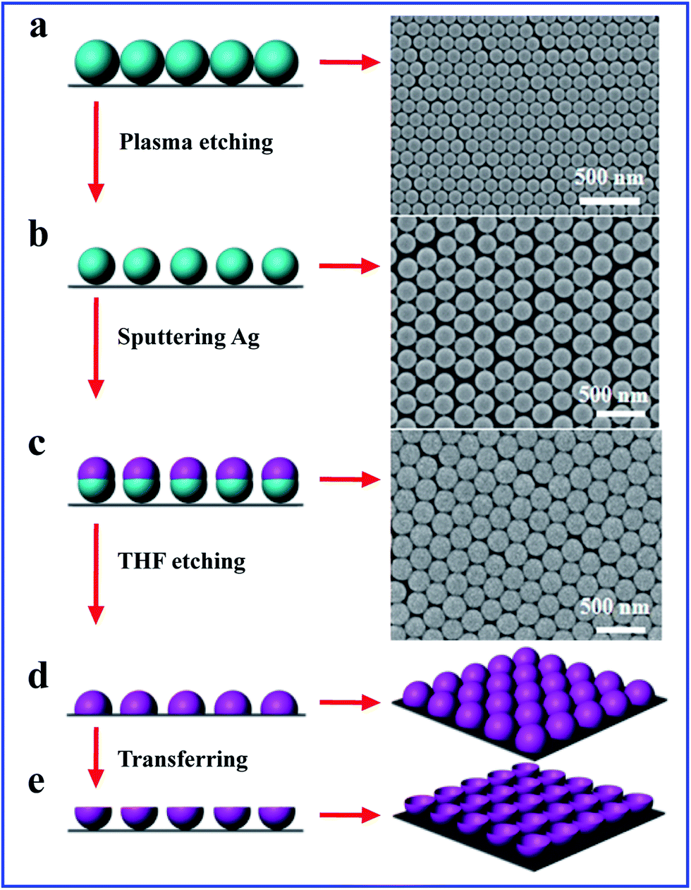
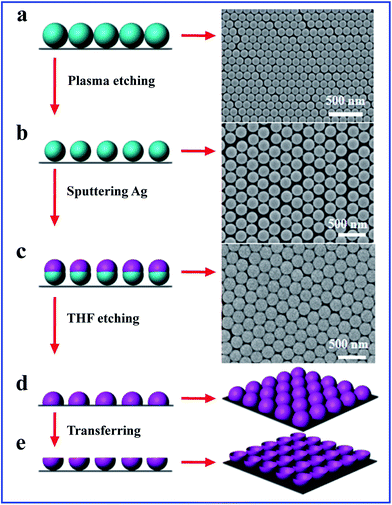
The fabrication process and the SEM images for the silver nanobowl arrays are illustrated in Fig. 1. Firstly, the monolayer close-packed 2D PS templates with diameter of 200 nm are prepared on Si wafer by NSL method (Fig. 1a). The corresponding SEM image exhibits a hexagonal close-packed array. Then these close-packed PS arrays are etched for different time by plasma etching technique (Fig. 1b). The diameter of the PS bead decreases gradually when oxygen plasma etching goes on. The period and shape of the bead array are maintained and the bead surfaces are still smooth upon etching. When the etching time is 30 s, the neighbor beads are separated slightly, and the nanogap between adjacent PS is about 20 nm. When the etching time is 60 s, the neighbor beads are separated completely and the PS size is 160 nm with the gap around 40 nm. When Ag film is deposited on the PS nanosphere arrays to form Ag nanocaps arrays (Fig. 1c), then the PS nanospheres were removed by immersing the samples into tetrahydrofuran (THF) solution (Fig. 1d). Ag nanobowl arrays are finally obtained by transferring the Ag film onto a new substrate as shown in Fig. 1e. Based on the close-packed and separated PS beads array, the connected and separated nanobowls arrays are fabricated.
 |
| | Fig. 1 Schematic and the SEM images for the fabrication process of silver nanobowl arrays. (a) Original PS array. (b) Etched PS array. (c) Ag nanocap deposited on the PS template. (d) Ag nanocap array etched by THF. (e) Ag nanobowl array transferred on a new substrate. | |
Fig. 2 shows the SEM images of closed-packed nanobowl arrays based on PS array without etching when 80 nm Ag film is deposited onto PS 200 nm templates. The diameter of the Ag nanobowl is about 200 nm. The brims of the nanobowls are very thin and there are six notches in every nanobowl due to the shadow effect from the neighbor PS beads (Fig. 2a), as we have seen clearly in the inset. When 30 s etching is performed, the isolated Ag nanobowls with smooth brim form and no notches between adjacent bowls are observed (Fig. 2b). The tilted view of Ag nanobowl is given in enlarged inset of Fig. 2b, confirming the complete nanobowl shape. However, the morphology of Ag nanobowl based on the PS array etched for 60 s changes obviously. The nanoholes-like arrays with 200 nm period are observed (Fig. 2c). The film thickness and the PS diameter are almost equal when 80 nm Ag film is deposited onto PS arrays with diameter 120 nm with 60 nm gaps. In this case, the distances between the etched PS beads are so large that the shadow effect is reduced and therefore the Ag film between the PS beads connects the nanobowls together to become pro-continuous. Therefore, the nanobowl looks like holes embedded in a continuous film. Near the crack in the film, the nanobowls are observed, which confirms the nanobowl formation in the inset. Therefore, to further test the speculation, Ag film with the thickness of 100 nm is also deposited onto 200 nm PS beads after 60 s etching. The image of SEM shows the nanobowls are connected together more and the nanohole array form in which the hole size becomes smaller (Fig. 2d). The above results show the size of bowl rim and distance of neighborhood bowl can be modified easily by adjusting the PS diameter and the film thickness.
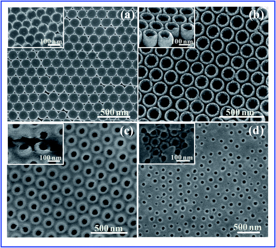 |
| | Fig. 2 SEM images of 80 nm Ag nanobowl array on O2-plasma etched PS for different times (a) 0 s, (b) 30 s, (c) 60 s, and (d) the 100 nm Ag nanobowl arrays on O2-plasma etched PS for 30 s. The insets are cross sectional views. | |
3.2 The SERS effect for nanobowl arrays
Fig. 3A shows the effects of different nanobowl morphologies on SERS enhancement in Ag nanobowl array. The main peaks located at 1614 cm−1, 1589 cm−1 and 1100 cm−1, which are assigned to C–C stretching mode, C–C stretching mode and C–S stretching mode,24 respectively. Compared to other samples, the largest SERS enhancement is observed on the isolated Ag nanobowl array based on PS template etched for 30 s, the reason is that the hot-spots in the nanogaps between adjacent nanobowls generate high plasma coupling, causing the SERS enhancement. Fig. 3B clearly shows the above changing trend. For the close-packed nanobowl array (Fig. 3a), the SERS enhancement is lower than the separated nanobowl (Fig. 3b), but higher than the hole-like array (Fig. 3c and d), which is ascribed to the sharp brim of nanobowl array. For the isolated nanocaps on the etched PS, the localized surface plasmons (LSPs) form and the plasmon coupling between the neighbor nanobowls contributes to the SERS enhancement. For the hole-like array, the localized surface plasma is extended and the couplings between the neighbors are reduced due to the connection of the neighbor Ag nanobowls, which leads to the decrease of the SERS signals.
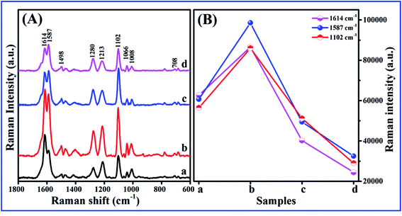 |
| | Fig. 3 (A) SERS spectra of the 4-MPy and (B) comparison of Raman intensities at v 1614 cm−1, 1587 cm −1, 1102 cm−1 on 80 nm Ag nanobowls etched for different times: (a) 0 s, (b) 30 s, (c) 60 s, (d) 100 nm Ag nanobowl arrays etched for 60 s. | |
To verify the contributions of the plasmon coupling between the interior and exterior Ag layers in nanobowl structure, the nanobowl arrays of sandwich structure Ag 40 nm/SiO2 t nm/Ag 40 nm (t = 0, 1, 2, 3) are fabricated on 200 nm PS substrate after etching for 30 s. The SiO2 layers with thickness from 1 to 3 nm are used to separate the Ag layer. Compared to isolated Ag nanobowl array without SiO2 spacer layer, Fig. 4a–d shows the SERS peaks of Ag 40 nm/SiO2 t nm/Ag 40 nm nanobowl (t = 0, 1, 2, 3) exhibit significant SERS enhancement. The SERS enhancement reaches the maximum when SiO2 thickness is 2 nm, which indicates that the plasma coupling occurs between interior Ag layer and exterior Ag layer through the SiO2 layer. The thin SiO2 layer is essential to transfer the strong electromagnetic field from its lower Ag layer to the upper Ag layer,32,33 which is an important factor leading to SERS enhancement. As a dielectric gap, the thin SiO2 layer could be used to tune the LSPs of the Ag layer in Ag/SiO2/Ag nanobowls,34 resulting in optimized LSPR interaction.
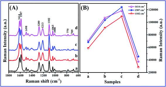 |
| | Fig. 4 (A) SERS spectra of the 4-MPy and (B) comparison of Raman intensities at 1614 cm−1, 1587 cm−1, 1102 cm−1 obtained on different samples: (a) Ag 80 nm nanobowl array without etched, Ag 40 nm/SiO2 t nm/Ag 40 nm nanobowl array with different thickness of SiO2 film: (b) 1, (c) 2, (d) 3. | |
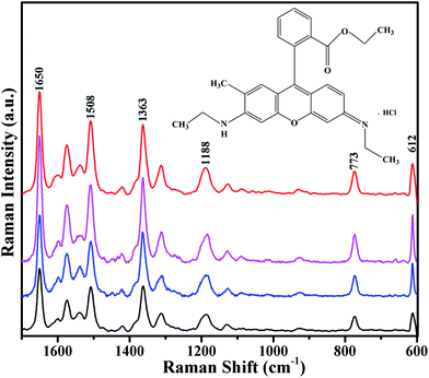
To verify the general applicability of the fabricated samples as the SERS substrates, we immersed the Ag 40 nm/SiO2 2 nm/Ag 40 nm arrays (t = 0, 1, 2, and 3) in an ethanol solution of 10−6 M R6G for 1 h. Raman spectra of the surfaces were collected with the same methods as above. Fig. 5 shows the characteristic Raman signals of R6G molecules with different samples: (a) Ag 80 nm nanobowl array without etched, Ag 40 nm/SiO2 t nm/Ag 40 nm nanobowl array with different thickness of SiO2 film: (b) 1, (c) 2, and (d) 3. All the Raman bands match well with those of the characteristic spectrum of R6G as followings.35 The peaks of 1650, 1508, 1363, 1188, 773 and 612 cm−1 are attributed to C–H in-plane bending, C–O–C stretching, C–C stretching of the aromatic ring, C–H in-plane bending, C–H out-of-plane bending and C–C–C in-plane bending modes, respectively.36,37 Compared to the peak intensities between different substrates, significantly, the highest Raman peak intensities can be clearly observed for the Ag 40 nm/SiO2 2 nm/Ag 40 nm arrays (Fig. 5c). Combining the above SERS spectra (Fig. 4) and this experimental SERS result, which further demonstrates the Ag 40 nm/SiO2 2 nm/Ag 40 nm arrays have good SERS performance.
 |
| | Fig. 5 SERS spectra of different samples: (a) Ag 80 nm nanobowl array without etched, Ag 40 nm/SiO2 t nm/Ag 40 nm nanobowl array with different thickness of SiO2 film: (b) 1, (c) 2, and (d) 3. | |
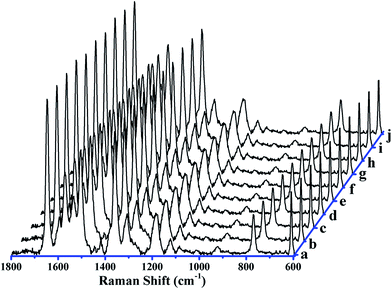
For any new SERS substrates, the reproducibility of Raman signals is an important factor. Fig. 6 shows the SERS spectra of the Ag 40 nm/SiO2 2 nm/Ag 40 nm arrays, which was collected from 10 random positions of the substrates. The relative standard deviation (RSD) of SERS intensity at the band of the 1650 cm−1 reaches to less than 6.4%, indicating the good reproducibility of the SERS substrates.
 |
| | Fig. 6 The reproducibility of SERS spectra for the Ag 40 nm/SiO2 2 nm/Ag 40 nm nanobowl array. | |
3.3 Characterization of nanobowl arrays
To further verify the chemical compositions of films, XPS measurements for the Ag 40 nm/SiO2 2 nm/Ag 40 nm arrays were performed. The XPS spectra of the full-scan spectrum, Ag 3d, Si 2p, O 1s and C 1s from films are shown in Fig. 7A–E, respectively. Fig. 7A shows that the full-scan XPS spectrum (0–1000 eV) of Ag/SiO2/Ag films, the peaks of Ag, Si, C and O have appeared. It is important to point out that the presence of C 1s (284.68 eV) may be due to the carbon tape used during the measurements, which is generally used as an internal reference in the spectra (Fig. 7E). Fig. 7B depicts that the two distinct peaks for Ag correspond to the Ag 3d5/2 and Ag 3d3/2 orbitals, which possess a doublet laid on 368.46 eV and 374.46 eV, respectively. The distinct peak of Si 2p locate at 103.3 eV was shown Fig. 7C. No evidence of the single Si peak was observed, which confirmed that Si exit only in the oxidized state SiO2 rather than from Si substrates. Fig. 7D shows the O 1s XPS spectrum of the sample, which can be deconvolved into the two strong peaks, indicating the existence of two different oxygen environments.38,39 The higher binding energy at 532.81 eV originates from the Si–O bond formation, one peak with a lower binding energy of 531.49 eV derives from the surface adsorbed oxygen, which is possibly attributed to environmental moisture trapped on the film surface.
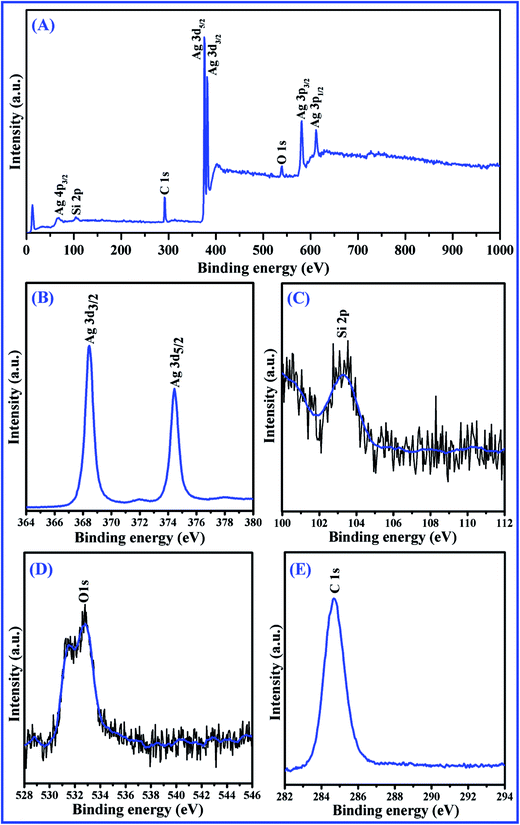 |
| | Fig. 7 The XPS spectra of (A) the full-scan spectrum, (B) Ag 3d, (C) Si 2p, (D) O 1s, and (E) C 1s of Ag 40 nm/SiO2 2 nm/Ag 40 nm nanobowl arrays. | |
3.4 SERS enhancement factor of Ag and Ag/SiO2/Ag nanobowl arrays
The EF is defined as EF = (ISERS × Nvol)(IRS × Nsurf),40–42 where ISERS and IRS are the intensities of the band 1614 cm−1 from the SERS substrates and reference solution (1 × 10⁻³ M), respectively. Nvol = CRSV is the average number of molecules in the scattering volume (V) for the Raman (non-SERS) measurement and Nsurf is the average number of adsorbed molecules in the scattering volume for the SERS experiments. The 4-MPy forms a homogeneous monolayer on the substrate after absorption (Fig. S4†), and the surface area occupied by single 4-Mpy molecule on the silver substrate value is estimated to be 0.30 nm2.2,43,44 The laser spot is a circle with a diameter of 1 μm. Nsurf can be calculated to be 2 × 10⁵. For the optical configuration and microscope employed, the effective focused depth is 1 μm. Nvol = CRSV is about 4.7 × 10⁹. So the EF is calculated to be 1.37 × 10⁷ and 8 × 10⁷ for Ag/SiO2/Ag nanobowl arrays when SiO2 thickness is 1 nm and 2 nm, and 7.5 × 10⁵ for Ag (80 nm) nanobowl and 2.8 × 10⁶ when SiO2 thickness is 3 nm.
3.5 FDTD solutions
The SERS enhancement was explained from the electromagnetic field distribution and charge density distribution for the different nanobowl arrays, as shown in Fig. 7. The local field enhancement of the vertical cross sections of the nanobowls with Ag thickness 80 nm and Ag 40 nm/SiO2 2 nm/Ag 40 nm nanobowls on silicon substrate was simulated by FDTD solutions. All plots of the data are shown for the x–z vertical cross sections containing the center of the nanobowl arrays. The simulation models of Ag and Ag/SiO2/Ag nanobowl arrays are shown in Fig. 8d and e, respectively. Fig. 8a shows that the resonances for nanobowls corresponding to the close-packed nanobowls with Ag thickness 80 nm, as we can see, the enhanced field is ascribed to the plasmon couplings between vertexes of the Ag nanobowl arrays (g1), the gap plasmons at the crevice nanogap regions (2 nm) (g2) and the LSPs between Ag nanobowl and the substrate (g3). The charge density distribution plots (in right column) show distinct SPR between Ag nanobowls, which confirms that the resonance belongs to quadrupole resonance mode in essence.45 Fig. 8b shows that the resonances for the separated Ag nanobowls, and the strongly enhanced local field is confined to the very narrow nanogap regions at the separated Ag nanobowl arrays (g2) and the LSPs between Ag nanobowl and the substrate (g3). The charge distribution is supporting a symmetrical dipole resonance mode. The resonances for the Ag 40 nm/SiO2 2 nm/Ag 40 nm nanobowls were shown in Fig. 8c. From the point of the E-field distribution, we think that the field enhancements can be mainly attributed to the SPPs of interparticles that propagate along the Ag–SiO2 interfaces (g4),46 in addition to the contributions of the gaps between Ag/SiO2/Ag nanobowls (g2) and the LSPs between Ag nanobowl and the substrate (g3). By comparing the FDTD simulation of the Ag nanobowl arrays (Fig. 8b), the electromagnetic field experiences a change, resulting in an extra distribution of the electromagnetic field between the Ag layer and Ag layer. The presence of the dielectric SiO2 layer provides an additional field confinement in the hot spot for the case of the new, quadrupolar plasmon mode.47 Strong SPR between Ag/SiO2/Ag nanobowls confirms that the resonance belongs to symmetrical dipole resonance mode. It is clear that adding insulator SiO2 layer can increase the substrate's SERS activity, and there exists an optimal SiO2 thickness for the maximal Raman enhancement.
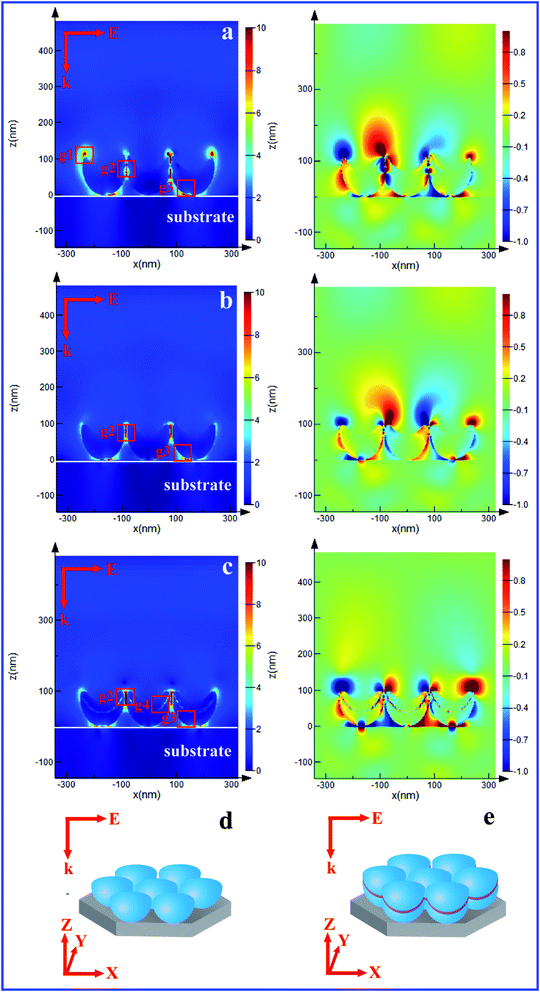 |
| | Fig. 8 Electric field distribution in left column and charge density distribution in right column for different nanobowls excited at 514.5 nm laser wavelength. (a) Close-packed Ag 80 nm nanobowl array etched for 0 s. (b) Separated Ag 80 nm nanobowl array etched for 30 s. (c) Separated Ag 40 nm/SiO2 2 nm/Ag 40 nm nanobowls etched for 30 s. The color bar represents the value of |E|/|Eo|. (d) The simulation model image of Ag nanobowl array. (e) The simulation model image of Ag/SiO2/Ag nanobowl array. | |
4. Conclusions
In conclusion, the nanobowls or nanohole-like arrays of Ag and Ag/SiO2/Ag with different morphologies are successfully fabricated by the combination of NSL technology and LBL film deposition. The morphologies are modified by changing the film thickness and the size of PS beads. In contrast to the nanohole-like array, the nanobowl array exhibits stronger SERS signal, which is ascribed to two important factors. One is that the gaps between adjacent PS or sharp edges around rims contribute to the SERS enhancement. The other is that the plasma coupling at the bowl bottom gaps between the interior and exterior surface of nanobowl structure also contributes to the high SERS signal, as verified by Ag/SiO2/Ag nanobowl structure.
Conflicts of interest
There are no conflicts to declare.
Acknowledgements
This work is supported by the National Natural Science Foundation of China (No. 61575080, 61675090 and 21676115), National Youth Program Foundation of China (No. 21546013, 61405072 and 51609100), Program for the development of Science and Technology of Jilin province (No. 20150519024JH, 20150520015JH, 20160101287JC and 20140519003JH), and Technology of Education Department of Jilin Province (No. 2016-217).
References
- M. Fleischmann, P. J. Hendra and A. J. McQuillan, Ramanspectra of pyridine adsorbed at silver electrode, Chem. Phys. Lett., 1974, 26, 163–166 CrossRef CAS.
- J. Chen, B. Shen, G. Qin, X. Hu, L. Qian, Z. Wang, S. Li, Y. Ren and L. Zuo, Fabrication of large-area, high-enhancement SERS substrates with tunable interparticle spacing and application in identifying microorganisms at the single cell level, J. Phys. Chem. C, 2012, 116, 3320–3328 CAS.
- M. Bechelany, P. Brodard, J. Elias, A. Brioude, J. Michler and L. Philippe, Simple synthetic route for SERS-active gold nanoparticles substrate with controlled shape and organization, Langmuir, 2010, 26, 14364–14371 CrossRef CAS PubMed.
- J. Theiss, P. Pavaskar, P. M. Echternach, R. E. Muller and S. B. Cronin, Plasmonic nanoparticle arrays with nanometer separation for high-performance SERS substrates, Nano Lett., 2010, 10, 2749–2754 CrossRef CAS PubMed.
- A. Barhoumi and N. J. Halas, Label-free detection of DNA hybridization using surface enhanced Raman spectroscopy, J. Am. Chem. Soc., 2010, 132, 12792–12793 CrossRef CAS PubMed.
- S. L. Kleinman, E. Ringe, N. Valley, K. Wustholz, E. Phillips, K. Scheidt, G. Schata and R. P. Van Duyne, Single-molecule surface-enhanced Raman spectroscopy of crystal violet isotopologues: theory and experiment, J. Am. Chem. Soc., 2011, 133, 4115–4122 CrossRef CAS PubMed.
- L. Chen, H. H. Sun, Y. Zhao, Y. J. Zhang, Y. X. Wang, L. Yang, X. L. Zhang, Y. H. Jiang, Z. Hua and J. H. Yang, Plasmonic-induced SERS enhancement of shell-dependent Ag@Cu2O core-shell nanoparticles, RSC Adv., 2017, 7, 16553–16560 RSC.
- L. Chen, Y. Zhao, Y. J. Zhang, M. M. Liu, Y. X. Wang, X. Qu, L. Yang, J. Li, X. Y. Liu and J. H. Yang, Design of Cu2O-Au composite microstructures for surface-enhanced Raman scattering study, Colloids Surf., A, 2016, 507, 96–102 CrossRef CAS.
- K. D. Alexander, K. Skinner, S. Zhang, H. Wei and R. Lopez, Tunable SERS in gold nanorod dimers through strain control on an elastomeric substrate, Nano Lett., 2010, 10, 4488–4493 CrossRef CAS PubMed.
- M. A. Noginov, G. Zhu, A. M. Belgrave, R. Bakker, V. M. Shalaev, E. E. Narimanov, S. Stout, E. Herz, T. Suteewong and U. Wiesner, Demonstration of a spaser-based nanolaser, Nature, 2009, 460, 1110–1112 CrossRef CAS PubMed.
- L. S. Slaughter, Y. P. Wu, B. A. Willingham, P. Nordlander and S. Link, Effects of symmetry breaking and conductive contact on the plasmon coupling in gold nanorod dimmers, ACS Nano, 2010, 4, 4657–4666 CrossRef CAS PubMed.
- T. Liu, D. S. Li, Y. Zou, D. R. Yang, H. L. Li, Y. M. Wu and M. H. Jiang, Preparation of metal @ silica core–shell particle films by interfacial self-assembly, J. Colloid Interface Sci., 2010, 350, 58–62 CrossRef CAS PubMed.
- Q. Fu, Z. B. Zhan, J. X. Dou, X. Z. Zheng, R. Xu, M. H. Wu and Y. Lei, Highly reproducible and sensitive SERS substrates with Ag inter-nanoparticle gaps of 5 nm fabricated by ultrathin aluminum mask technique, ACS Appl. Mater. Interfaces, 2015, 7, 13322–13328 CAS.
- H. Lange, B. H. Juárez, A. Carl, M. Richter, N. G. Bastús, H. Weller, C. Thomsen, R. V. Klitzing and A. Konrr, Tunable plasmon coupling in distance-controlled gold nanoparticles, Langmuir, 2012, 28, 8862–8866 CrossRef CAS PubMed.
- G. Q. Liu, Y. Li, G. T. Duan, J. J. Wang, C. H. Liang and W. P. Cai, Tunable surface plasmon resonance and strong SERS performances of Au opening-nanoshell ordered arrays, ACS Appl. Mater. Interfaces, 2011, 4, 1–5 Search PubMed.
- L. Gunnarsson, E. J. Bjerneld, H. Xu, S. Petronis, B. Kasemo and M. Kall, Interparticle coupling effects in nanofabricated substrates for surface-enhanced Raman scattering, Appl. Phys. Lett., 2001, 78, 802–804 CrossRef CAS.
- A. Gopinath, S. V. Boriskina, W. R. Premasiri, L. Ziegler, B. M. Reinhard and L. D. Negro, Plasmonic nanogalaxies: multiscale aperiodic arrays for surface-enhanced Raman sensing, Nano Lett., 2009, 9, 3922–3929 CrossRef CAS PubMed.
- S. Y. Chou, P. P. Krauss and P. J. Renstrom, Nanoimprint lithography, J. Vac. Sci. Technol., B: Microelectron. Nanometer Struct., 1996, 14, 4129–4133 CrossRef CAS.
- Y. X. Wang, X. Y. Zhao, L. Chen, S. Chen, M. B. Wei, M. Gao, Y. Zhao, C. Wang, X. Qu, Y. J. Zhang and J. H. Yang, Ordered nanocap array composed of SiO2-isolated Ag islands as SERS platform, Langmuir, 2014, 30, 15285–15291 CrossRef CAS PubMed.
- K. Chen, B. B. Rajeeva, Z. L. Wu, M. Rukavina, T. D. Dao, S. Ishii, M. Aono, T. Nagao and Y. B. Zheng, Moiré nanosphere lithography, ACS Nano, 2015, 9, 6031–6040 CrossRef CAS PubMed.
- J. Yu, C. Geng, L. Zheng, Z. H. Ma, T. Y. Tan, X. Q. Wang, Q. F. Yan and D. Z. Shen, Preparation of high-quality colloidal mask for nanosphere lithography by a combination of air/water interface self-assembly and solvent vapor annealing, Langmuir, 2012, 28, 12681–12689 CrossRef CAS PubMed.
- A. B. Zrimsek, A. I. Henry and R. P. Van Duyne, Single molecule surface-enhanced Raman spectroscopy without nanogaps, J. Phys. Chem. Lett., 2013, 4, 3206–3210 CrossRef CAS.
- L. Ji, Y. F. Chang, B. Fowler, Y. C. Chen, T. M. Tsai, K. C. Chang, M. C. Chen, T. C. Chang, S. M. Sze, E. T. Yu and J. C. Lee, Integrated one diode–one resistor architecture in nanopillar SiOx resistive switching memory by nanosphere lithography, Nano Lett., 2013, 14, 813–818 CrossRef PubMed.
- Y. X. Wang, X. Y. Zhao, W. T. Gao, L. Chen, S. Chen, M. B. Wei and M. Gao, Au/Ag bimetal nanogap arrays with tunable morphologies for surface-enhanced Raman scattering, RSC Adv., 2015, 5, 7454–7460 RSC.
- C. X. Wang, W. D. Ruan, N. Ji, W. Ji, S. Lv, C. Zhao and B. Zhao, Preparation of nanoscale Ag semishell array with tunable interparticle distance and its application in surface-enhanced Raman scattering, J. Phys. Chem. C, 2010, 114, 2886–2890 CAS.
- X. Y. Zhao, J. H. Wen, M. N. Zhang, D. H. Wang, Y. X. Wang, L. Chen, Y. J. Zhang, J. H. Yang and Y. W. Du, Design of Hybrid Nanostructural Arrays to Manipulate SERS-Active Substrates by Nanosphere Lithography, ACS Appl. Mater. Interfaces, 2017, 9, 7710–7716 CAS.
- T. Y. Jeon, S. G. Park, S. Y. Lee, H. C. Jeon and S. M. Yang, Shape control of Ag nanostructures for practical SERS substrates, ACS Appl. Mater. Interfaces, 2013, 5, 243–248 Search PubMed.
- D. D. Lin, Z. L. Wu, S. J. Li, W. Q. Zhao, C. J. Ma, J. Wang, Z. M. Jiang, Z. Y. Zhong, Y. B. Zheng and X. J. Yang, Large-Area Au-Nanoparticle-Functionalized Si Nanorod Arrays for Spatially Uniform Surface-Enhanced Raman Spectroscopy, ACS Nano, 2017, 11, 1478–1487 CrossRef CAS PubMed.
- L. Chen, H. H. Sun, Y. Zhao, R. X. Gao, Y. X. Wang, Y. Liu, Y. J. Zhang, Z. Hua and J. H. Yang, Iron Layer-Dependent Surface-Enhanced Raman Scattering of Hierarchical Nanocap Arrays, Appl. Surf. Sci., 2017, 423, 1124–1133 CrossRef CAS.
- Y. J. Zhang, C. Wang, J. Wang, J. P. Wang, L. Chen, J. Li, Y. Liu, X. Y. Zhao, Y. X. Wang and J. H. Yang, Nanocap array of Au: Ag composite for surface-enhanced Raman scattering, Spectrochim. Acta, Part A, 2016, 152, 461–467 CrossRef CAS PubMed.
- S. Siddhanta, V. Thakur, C. Narayana and S. M. Shivaprasad, Universal metal- semiconductor hybrid nanostructured SERS substrate for biosensing, ACS Appl. Mater. Interfaces, 2012, 4, 5807–5812 CAS.
- J. F. Li, Y. F. Huang, Y. Ding, Z. L. Yang, S. B. Li, X. S. Zhou, F. R. Fan, W. Zhang, Z. Y. Zhi, D. Y. Wu, B. Ren, Z. L. Wang and Z. Q. Tian, Shell-isolated nanoparticle-enhanced Raman spectroscopy, Nature, 2010, 464, 392–395 CrossRef CAS PubMed.
- H. Miyazaki and Y. Kurokawa, Squeezing visible light waves into a 3-nm-thick and 55-nm-long plasmon cavity, Phys. Rev. Lett., 2006, 96, 097401 CrossRef PubMed.
- T. K. Liu, M. S. Tsai, W. C. Hung, C. T. Kuo, D. P. Wang and I. M. Jiang, Field-enhanced Raman scattering by silver nanoparticle with graded SiO2 coating, Appl. Phys. Lett., 2013, 102, 153105 CrossRef.
- P. Hildebrandt and M. Stockburger, Surface-enhanced resonance Raman spectroscopy of Rhodamine 6G adsorbed on colloidal silver, J. Phys. Chem., 1984, 88, 5935–5944 CrossRef CAS.
- M. Liu, L. Sun, C. W. Cheng, H. L. Hu, Z. X. Shen and H. J. Fan, Highly effective SERS substrates based on an atomic-layer-deposition-tailored nanorod array scaffold, Nanoscale, 2011, 3, 3627–3630 RSC.
- C. Y. Niu, B. F. Zou, Y. Q. Wang, C. Lin, H. H. Zheng and S. M. Zhou, Highly Sensitive and Reproducible SERS Performance from Uniform Film Assembled by Magnetic Noble Metal Composite Microspheres, Langmuir, 2016, 32, 858–863 CrossRef CAS PubMed.
- M. Chen, X. Wang, Y. H. Yu, Z. L. Pei, X. D. Bei, C. Sun, R. F. Huang and L. S. Wen, X-ray photoelectron spectroscopy and auger electron spectroscopy studies of Al-doped ZnO films, Appl. Surf. Sci., 2000, 158, 134–140 CrossRef CAS.
- Z. Hua, Y. P. Song, Y. R. Sui, Y. J. Wu, S. Q. Lv, B. Yao, L. Xiao, Z. W. Wang and X. Y. Liu, Effect of Ar/O2 gas ratios on the structure, electrical and optical properties of Na-doped ZnCdO film synthesized by magnetron sputtering, J. Mater. Sci.: Mater. Electron., 2016, 27, 8745–8752 CrossRef CAS.
- Y. L. Wang, X. Q. Zou, W. D. Ren, W. D. Wang and E. Wang, Effect of silver nanoplates on Raman spectra of p-aminothiophenol assembled on smooth macroscopic gold and silver surface, J. Phys. Chem. C, 2007, 111, 3259–3265 CAS.
- B. Ren, X. F. Lin, Z. L. Yang, G. K. Liu, R. F. Aroca, B. W. Mao and Z. Q. Tian, Surface-enhanced Raman scattering in the ultraviolet spectral region: UV-SERS on rhodium and ruthenium electrodes, J. Am. Chem. Soc., 2003, 125, 9598–9599 CrossRef CAS PubMed.
- S. M. Zhu, C. Z. Fan, J. Q. Wang, J. N. He, E. Liang and M. J. Chao, Surface enhanced Raman scattering of 4-aminothiophenol sandwiched
between Ag nanocubes and smooth Pt substrate: The effect of the thickness of Pt film, J. Appl. Phys., 2014, 116, 044312 CrossRef.
- T. V. Teperik, V. V. Popov and F. J. De Abajo, Void plasmons and total absorption of light in nanoporous metallic films, Phys. Rev. B: Condens. Matter Mater. Phys., 2005, 71, 085408 CrossRef.
- W. B. Cai, B. Ren, X. Q. Li, C. X. She, F. M. Liu, X. W. Cai and Z. Q. Tian, Investigation of surface-enhanced Raman scattering from platinum electrodes using a confocal Raman microscope: dependence of surface roughening pretreatment, Surf. Sci., 1998, 406, 9–22 CrossRef CAS.
- M. Frederiksen, V. E. Bochenkov, M. B. Cortie and D. S. Sutherland, Plasmon hybridization and field confinement in multilayer metal–dielectric nanocups, J. Phys. Chem. C, 2013, 117, 15782–15789 CAS.
- J. Lee, Q. P. Zhang, S. Y. Park, A. Choe, Z. Y. Fan and H. Ko, Particle–film plasmons on periodic silver film over nanosphere (AgFON): a hybrid plasmonic nanoarchitecture for surface-enhanced Raman spectroscopy, ACS Appl. Mater. Interfaces, 2015, 8, 634–642 Search PubMed.
- F. F. Wen, J. Ye, N. Liu, P. V. Dorpe, P. Nordlander and N. J. Halas, Plasmon transmutation: inducing new modes in nanoclusters by adding dielectric nanoparticles, Nano Lett., 2012, 12, 5020–5026 CrossRef CAS PubMed.
Footnote |
| † Electronic supplementary information (ESI) available. See DOI: 10.1039/c7ra09690a |
|
| This journal is © The Royal Society of Chemistry 2017 |
Click here to see how this site uses Cookies. View our privacy policy here. 
 Open Access Article
 This Open Access Article is licensed under a Creative Commons Attribution-Non Commercial 3.0 Unported Licence
 ,
Yang Liu,
Yongjun Zhang* and
Jinghai Yang
,
Yang Liu,
Yongjun Zhang* and
Jinghai Yang