DOI:
10.1039/C7RA09668B
(Paper)
RSC Adv., 2017,
7, 51466-51474
Strain/stress engineering on the mechanical and electronic properties of phosphorene nanosheets and nanotubes
Received
31st August 2017
, Accepted 20th October 2017
First published on 6th November 2017
Abstract
Phosphorene is demonstrated to have a great potential in the electronics applications. In this work, the first-principle calculations are employed to predict the mechanical properties and the electronic structure of phosphorene nanosheets and nanotubes. Compared with that of nanosheets, the maximum tensile stress of nanotubes decreases from 17.66 GPa to 11.73 GPa in the zigzag direction and 7.56 GPa to 5.95 GPa in the armchair direction. The ultimate tensile strain of nanosheets is about 27% in the armchair and 25% in the zigzag directions. However, the maximum strain of the zigzag nanotubes decreases to 24% and the ultimate strain of the armchair nanotube is about 14.4%. It presents that the tensile modulus will decrease with the increasing tension, while the compression modulus increases with increasing compression. The results show that zigzag-direction stress will affect the covalent bonds largely, while the armchair-direction stress influences the lone-pair electrons more. Within the allowable strain, the band structure and effective mass of carriers are calculated. The CBM and VBM change their positions when the stress is applied. The effective mass of nanosheets and nanotubes is strongly affected by strain.
1. Introduction
Phosphorene, a two-dimensional material, was first obtained from black phosphorus (BP), whose layers were held together by weak van der Waals forces.1–5 In fact, BP was first synthesized in 1914 by Bridgman.6 Then, it took scientists exactly 100 years to prepare a one-atom-thick layer of phosphorus (named phosphorene) by mechanical exfoliation of bulk BP.7 In recent years, phosphorene has attracted large attention due to its potential applications in optoelectronics and electronics.8,9 Moreover, phosphorene is predicted to be a strong competitor to graphene because, in contrast to graphene, phosphorene has a narrow band gap.10 It has been proven that phosphorene has a thickness dependent direct band gap that changes from 0.3 eV in the bulk to 1.88 eV in a monolayer.11 Density functional calculations also showed that the increasing band-gap-value was caused by the absence of the interlayer hybridization near the top of the valence and the bottom of the conduction band.4 It was also reported that phosphorene has a carrier mobility up to 1000 cm2 V−1·s−1,1 while that of another two-dimensional material, MoS2, is only about 200 cm2 V−1·s−1.12 The mechanical behavior is one of the hot topics in the research about two-dimensional materials. For example, monolayer graphene was reported to have an intrinsic tensile strength of 130 GPa and a Young's modulus of 1 TPa13 through experiments. Monolayer MoS2 has a breaking strength of 16–30 GPa and a Young's modulus of 270 GPa.12 A theoretical simulation like density functional theory (DFT) or molecular dynamics is an effective method to predict the mechanical properties of nanomaterials. For example, borophene was calculated to hold an elastic stiffness of 210 N m−1.14 It was also theoretically demonstrated that monolayer phosphorene can hold a critical strain up to 30% and withstand stress up to 18 GPa in the zigzag direction and 8 GPa in the armchair direction.15 As we all know, for two-dimensional semiconductor materials like WS2 (ref. 16) and MoS2,17 their band structures are very sensitive to strain. It was also proven that the electronic structure of phosphorene was affected by strain. The band gap of phosphorene experiences a direct–indirect–direct transition when axial strain is applied.18 With the appropriate biaxial or uniaxial strain (4–6%), the preferred conducting direction can be rotated by 90°.19
As mentioned, great attention has been paid to investigate the strain engineered properties of phosphorene. In most cases, a small strain was employed to modulate the electronic properties of phosphorene. In contrast, the strain engineered properties of nanotubes have been rarely reported. In this study, phosphorene nanosheets and nanotubes are fully geometry optimized in a specific force field. First, we calculate the mechanical behavior of phosphorene nanosheets and nanotubes. Second, the effects of stress on the band structure of nanosheets and nanotubes are investigated. In the end, we discuss the effective mass of carriers in nanosheets and nanotubes under applied strain/stress.
2. Computational methodology
The first-principles DFT simulation is performed using the CASTEP module. We adopt the generalized gradient approximation (GGA) and the Perdew–Burke–Ernzerhof (PBE) exchange-correlation functional for the structural optimization and self-consistent total energy calculations. Electronic wave functions are expanded in a plane wave basis set with the kinetic energy cutoff of 180 eV. A 3 × 3 × 1 Monkhorst–Pack k-point mesh is used for the Brillouin zone integration in the monolayer phosphorene simulation. For nanotubes, Monkhorst–Pack k-point mesh is set to 1 × 1 × 3. The energy convergence criterion for the electronic wave function is set to be 10−5 eV. A vacuum layer of about 12 Å is employed to avoid the interactions between the slabs in the single-layer and nanotube phosphorene calculations using periodic boundary conditions. For the accuracy of the band-structure calculation, 0.001 Å−1 is used in the k-point separation.
3. Results and discussion
We first calculate the strain–stress relations of phosphorene nanosheets and nanotubes. Fig. 1 presents the top view of monolayer phosphorene under the stresses along the zigzag (σx) and armchair (σy) directions. The Brillouin zone path is set as F → G → B to investigate the changes of the band states along the zigzag and armchair directions. According to our calculation results, the relaxed lattice constants for single-layer phosphorene are a = 3.299 Å and b = 4.643 Å, which is in good agreement with other reports.18–20 Fig. 1(b) and (c) describe the shape changes of monolayer phosphorene when the zigzag- or armchair-direction stress is applied.
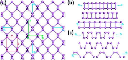 |
| | Fig. 1 (a) Top view of single-layer phosphorene when the stresses along the zigzag (σx) and armchair (σy) directions are added; “F → G → B” represents the Brillouin zone path. (b) The strain variation of single-layer phosphorene along the zigzag direction when σx = −17.66 GPa (top), σx = 0 (middle), and σx = 17.66 GPa (bottom). (c) The strain variation of single-layer phosphorene along the armchair direction when σy = −7.57 GPa (top), σy = 0 (middle), and σy = 7.82 GPa (bottom). σ (>0) represents the tensile stress; σ (<0) represents the compressive stress. | |
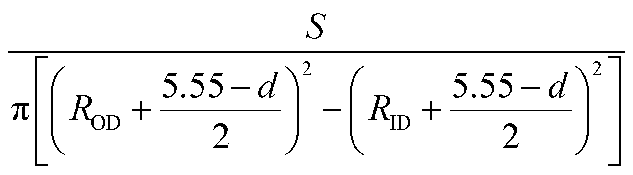
As shown in Fig. 2, the zigzag (12.0) and armchair (0.8) nanotubes are chosen for comparison. The Brillouin zone path of a nanotube is G → F → Q. Herein, we are only concerned with the electronic structure along F → Q. For the stratified material, the stress calculated from the DFT should be modified due to the vacuum between layers. The stress is rescaled by multiplying it by Z/d0 to obtain equivalent stress, where Z and d0 represent the cell length in the z-direction and the effective thickness, respectively. For monolayer phosphorene, d0 = 5.55 Å. For nanotubes, the stress is rescaled by  , where S is the XY plane area of the cell, ROD and RID represent the outer and inner radius of a nanotube, respectively, and d is the layered thickness of phosphorene.
 |
| | Fig. 2 Side view of a single-wall phosphorene nanotube with the stresses along the (a) zigzag and (b) armchair directions. (a) Armchair and (b) zigzag nanotubes are built by rolling up a (1.8) and (12.1) phosphorene sheet, respectively. “G → F → Q” represents the Brillouin zone path. | |
3.1 Mechanical behavior and band gap
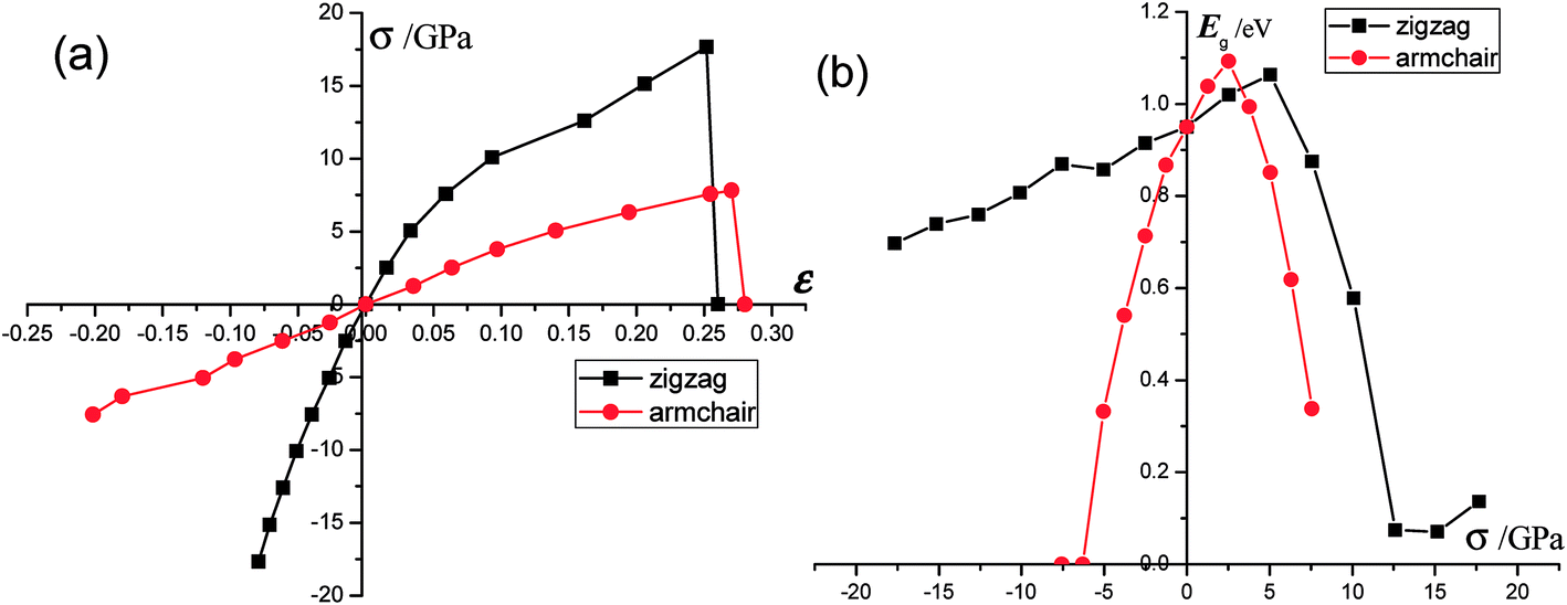
Phosphorene nanosheets. The strain–stress relations of single-layer phosphorene are plotted in Fig. 3(a). When stress is applied, monolayer phosphorene is able to withstand a tensile stress up to 17.66 GPa in the zigzag direction and 7.56 GPa in the armchair direction. These results agree well with those of other reports.15 According to our calculation, the ultimate tensile strain of monolayer phosphorene is about 27% in the armchair direction and 25% in the zigzag direction.18 Consequently, single-layer phosphorene exhibits different Young's modulus along different directions in a plane. It indicates its anisotropic nature.15 Elahi21 mentioned that the tensile strain from 0 to 27% can be viewed as the elastic region. According to our results, the Young's modulus of monolayer phosphorene along the zigzag (or armchair) direction is calculated to be 164.9 GPa (or 34.4 GPa). The theoretical predictions are very close to the experimentally measured values.22,23 In addition, the mechanical properties in phosphorene will change with the stress. During the tension progress, variations of Young's modulus in the zigzag direction fluctuate greatly; it decreases from 164.9 GPa to 55 GPa until fracture. For the armchair-direction tensile test, the Young's modulus fluctuates slightly and decreases from 34.4 GPa to 16 GPa until fracture. When the compression is applied in the axial direction, the changes of compression modulus in monolayer phosphorene behave in the same way. The zigzag-direction compression modulus increases from 168.2 GPa to 315.3 GPa. The armchair-direction compression modulus increases from 47.6 GPa to 58.7 GPa during the compression test. It should be noted that the compression modulus continually increases as the compression keeps rising. Fig. 3(b) presents the strain/stress induced band gap of phosphorene nanosheets. The band gap of single-layer phosphorene is 0.95 eV. These results are consistent with other theoretical predictions.24 As reported in ref. 25, the band gap of monolayer phosphorene measured through photoluminescence is about 1.75 eV. It is well-known that DFT may underestimate the band gaps of semiconductors. The HSE06 method gives consistently larger values for the band gaps of unstrained phosphorene. Based on HSE06, the band gap of unstrained phosphorene is calculated to be 1.55 eV. However, we mainly focus on the variation trend of the band gap in this study. For the zigzag-direction stress (σx), the band gap of monolayer phosphorene increases gradually as the stress changes from −17.66 GPa to 5.05 GPa. In stark contrast, the band gap drops sharply when the tensile stress grows from 5.05 GPa to 12.67 GPa. After this, a slight rise in the band gap appears until the material failure. It is clearly shown that the band gap peaks at 1.06 eV when the zigzag-direction stress is applied on monolayer phosphorene.26 However, the changes of the armchair-direction (σy) stress related band gap are a little different. Between −7.57 GPa and −6.31 GPa, single-layer phosphorene shows a nearly metallic behavior. The band gap increases dramatically when stress rises from −6.31 GPa to 2.52 GPa. Between 2.52 GPa and 7.57 GPa, there is a sharp decrease in the band gap. Interestingly, the greatest band gap (1.09 eV) induced by σy is quite close to that caused by σx.
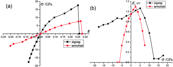 |
| | Fig. 3 (a) The strain–stress curves of monolayer phosphorene. The black line represents the strain changes under the zigzag-direction stress, while the red line describes the strain variation under the armchair-direction stress. According to our calculations, the maximum strain and stress of single-layer phosphorene are ε = 0.26 and σ = 17.66 GPa (the zigzag direction) and ε = 0.27 and σ = 7.82 GPa (the armchair direction). (b) The band gap of monolayer phosphorene changes with the stress. | |
To better understand the effects of stress on electronic structure, we calculate the electron localization function (ELF) of phosphorene nanosheets. As shown in Fig. 4, the electrons are packed together to describe the distribution of covalent bonds and lone pairs. When compression is applied in the zigzag direction (σx = −17.66 GPa), the electrons (as indicated by the black circle) exhibit a more highly concentrated distribution. It indicates that the repulsion between phosphorus atoms becomes stronger. Thus, phosphorene nanosheets become more and more difficult to be compressed. This is consistent with the increasing compression modulus as we mentioned earlier. In Fig. 4(c), when phosphorene withstands the ultimate tension stress (σx = 17.66 GPa), the local concentration of electrons decreases. It also indicates that, compared to that of lone pairs of electrons, the distribution of electrons that represent the covalent bonds becomes more disperse. As marked in the black circle, the electrons seem to be separated, suggesting the nearly broken bonds. Consequently, the tensile modulus decreases with increasing tension. It can be noted that the stress along the zigzag direction has large effects on the distribution of electrons, which represent the covalent bonds. The armchair-direction stress works in the same way. As shown in Fig. 4(d), the distribution of lone electrons changes dramatically. When compression is applied in the armchair direction (σy = −7.57 GPa), the lone electrons (as marked by the black circle), which belong to different atoms, repel each other. Moreover, when the tensile stress of σy = 7.57 GPa is applied, the concentration of lone electrons marked in the circle decreases. It also indicates that the interaction between non-bonding atoms decreases. We summarize that the zigzag-direction stress affects the covalent bonds largely, while the armchair-direction stress influences lone-pair electrons more.
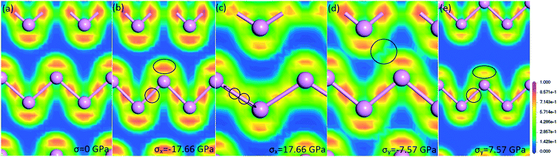 |
| | Fig. 4 The top-view ELF images of phosphorene nanosheets under different force fields. | |
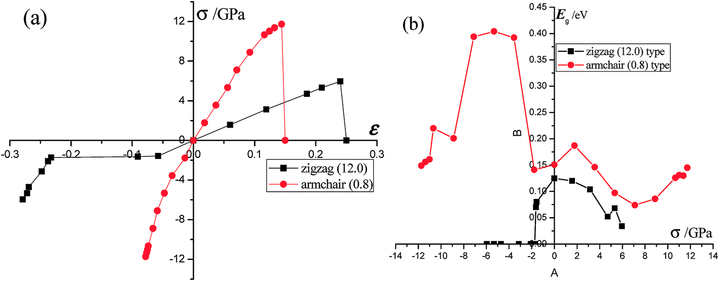
Phosphorene nanotubes. The strain–stress relations as well as the band gap changes of phosphorene nanotubes are presented in Fig. 5. Clearly, the zigzag (12.0) nanotube could withstand tensile stress up to 11.73 GPa, and the maximum tensile stress of the armchair (0.8) nanotube was about 5.95 GPa. The maximum strain of the zigzag (12.0) nanotube was about 24%, which is a little smaller than that of nanosheets in the armchair direction. Interesting enough, the ultimate strain of the armchair (0.8) nanotube is about 14.4%, which is well consistent with the result (15.5%) reported in ref. 27. However, it decreases considerably compared with the ultimate strain along the zigzag direction in nanosheets. For the zigzag (12.0) nanotube, the Young's modulus stabilizes at an average value of 25.6 GPa until it is broken. The Young's modulus of the zigzag (12.0) nanotube is close to that of the zigzag (14.0) nanotube (35.2 GPa) and zigzag (16.0) nanotube (41.7 GPa) reported in ref. 28. However, it is smaller than that of the nanosheets along the armchair direction (34.4 GPa). Within a large variation range, the Young's modulus of the armchair (0.8) nanotube decreases from 97.8 GPa to 30.2 GPa. It is different from that of the nanosheets along the zigzag direction. The compression modulus of the zigzag (12.0) nanotube decreases from 27.1 GPa to 8.2 GPa when the compression is between 0 GPa and −3.1 GPa and then increases from 8.2 GPa to 84.7 GPa when the compression is in the range −3.1–6.0 GPa. The compression modulus of the armchair (0.8) nanotube varies in the same trend. It decreases slowly from 128.1 GPa to 85.6 GPa at a compression of 0–1.8 GPa and then gradually increases from 85.6 GPa to 233.3 GPa at the compression of −1.8–11.7 GPa. Compared with that of nanosheets, the compression modulus of the zigzag (12.0) and armchair (0.8) nanotubes is smaller. The strain/stress related band gaps of nanotubes are calculated and presented in Fig. 5(b). The zigzag (12.0) nanotube exhibits metallicity with the applied compressions between −6 GPa and −3.1 GPa. Its band gap increases from 0 eV to 0.125 eV with the compressions between −3.1 GPa and 0 GPa. Furthermore, the band gap decreases from 0.125 eV to 0.052 eV with tensile stress varying between 0 GPa and 4.7 GPa and then increases from 0.052 eV to 0.068 eV at the tensile stress of 4.7–5.3 GPa. According to the results, the band gap of the zigzag (12.0) nanotube reaches the maximum value of 0.125 eV at 0 GPa. The strain (or stress) leads to the band gap decreasing in the zigzag (12.0) nanotube. Furthermore, the zigzag (12.0) nanotube is very sensitive to compression and it exhibits metallicity at a small compression. The function of strain/stress in the armchair (0.8) nanotube is complicated. The compression related band gap increases from 0.149 eV to 0.404 eV with some fluctuation. Furthermore, the band gap in the armchair (0.8) nanotube reaches the maximum value of 0.404 eV at −5.33 GPa. When tensile stress is applied, the band gap shows a large fluctuation.
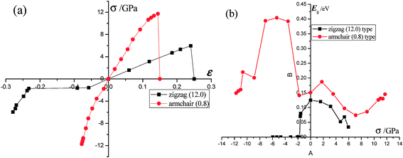 |
| | Fig. 5 (a) The strain–stress relationship of the zigzag/armchair phosphorene nanotube. The black line represents the changes of the strain in the zigzag nanotube under the armchair-direction stress. The red line represents the changes of the strain in the armchair nanotube under the zigzag-direction stress. According to our calculations, the maximum strain and stress of the zigzag phosphorene nanotube are ε = 0.24 and σ = 5.95 GPa and, for armchair nanotube, ε = 0.14 and σ = 11.73 GPa. (b) The band gap of the zigzag/armchair phosphorene nanotube changes with the stress. | |
As we discussed above, the mechanical behaviors in phosphorene nanosheets and nanotubes are very different. When compared with that of nanosheets, the ultimate tensile stress of nanotubes decreases from 17.66 GPa to 11.73 GPa in the zigzag direction and from 7.56 GPa to 5.95 GPa in the armchair direction. When being rolled into tubes, phosphorene holds the maximum strain decreasing from 27% to 24% in the armchair direction and 25–14.4% in the zigzag direction. Consequently, the mechanical performance of phosphorene decreases when rolled from nanosheets into nanotubes. Compared to other two-dimensional materials such as graphene, h-BN and MoS2, phosphorene sheets and nanotubes exhibit a superior flexibility with a much smaller Young's modulus (as shown in Table 1). For the strain induced band gap, phosphorene nanosheets demonstrate a better regularity than nanotubes. Furthermore, nanotubes hold a narrower band gap, which is consistent with the conclusion in ref. 29.
Table 1 Young's moduli of graphene, h-BN, MoS2, phosphorene sheets, and tubes
| |
|
Graphene13,30 |
h-BN30,31 |
MoS2 (ref. 32,33) |
Phosphorene15 |
| Young's moduli (TPa) |
Nanosheets |
1.0 |
1.1 |
0.33 |
0.166/0.044 |
| Nanotubes |
1.2(9,0) |
1.1(12,0) |
0.13(10,0) |
0.165/0.034 |
3.2 Band structure
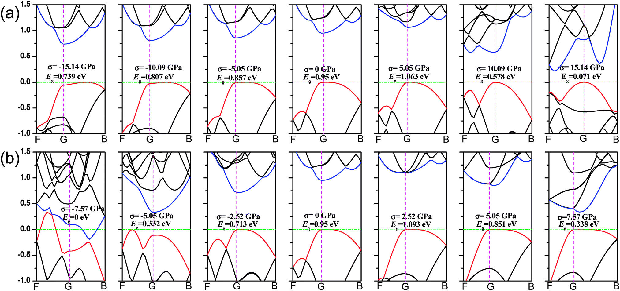
Phosphorene nanosheets. In this section, we focus on the shifts of the valence-band maximum (VBM) and the conduction-band minimum (CBM) produced by the stress. Fig. 6(a) presents the band structure of monolayer phosphorene when the zigzag-direction stress is applied. As mechanical compression of −15.14–0 GPa is applied along the zigzag direction, the position of VBM moves from B towards G. At the same time, the CBM located at G point moves and its values may increase with compression. With the compression decreasing, the band gap changes from an indirect type to a direct one. In case of tensile stress, the position of VBM remains unchanged and a new CBM is formed with the increasing tension. In Fig. 6(b), when the tensile stress is applied, the VBM of nanosheets stays at (0, G) and the CBM moves from G towards B. A new VBM will be formed when compression is applied. The CBM keeps its location at G point and its values decrease with the compression increasing. The band gap of monolayer phosphorene goes to zero when the armchair-direction compression is −7.57 GPa.
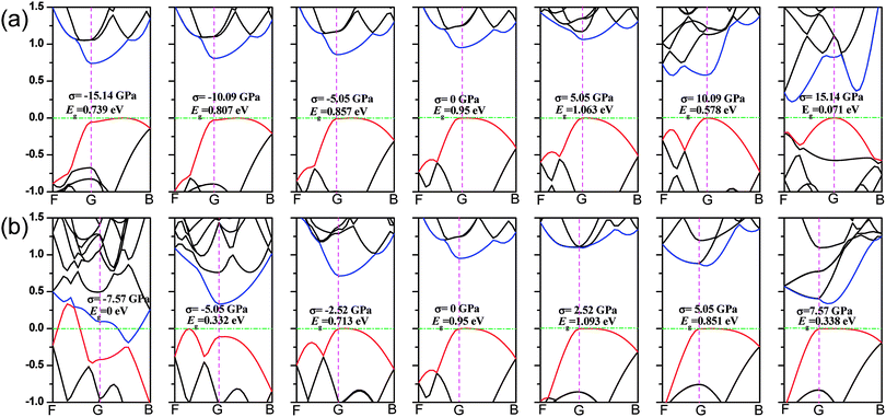 |
| | Fig. 6 (a) The band structure of monolayer phosphorene along F → G → B directions (when the stress is applied along the zigzag direction). The green dash lines describe the Fermi level. (b) The band structure of monolayer phosphorene along F → G → B directions (when the stress is added along the armchair direction). G is the Gamma point of the system. The blue lines represent the minimum conduction-band states and the red lines show the maximum valence-band states. | |
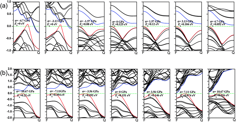
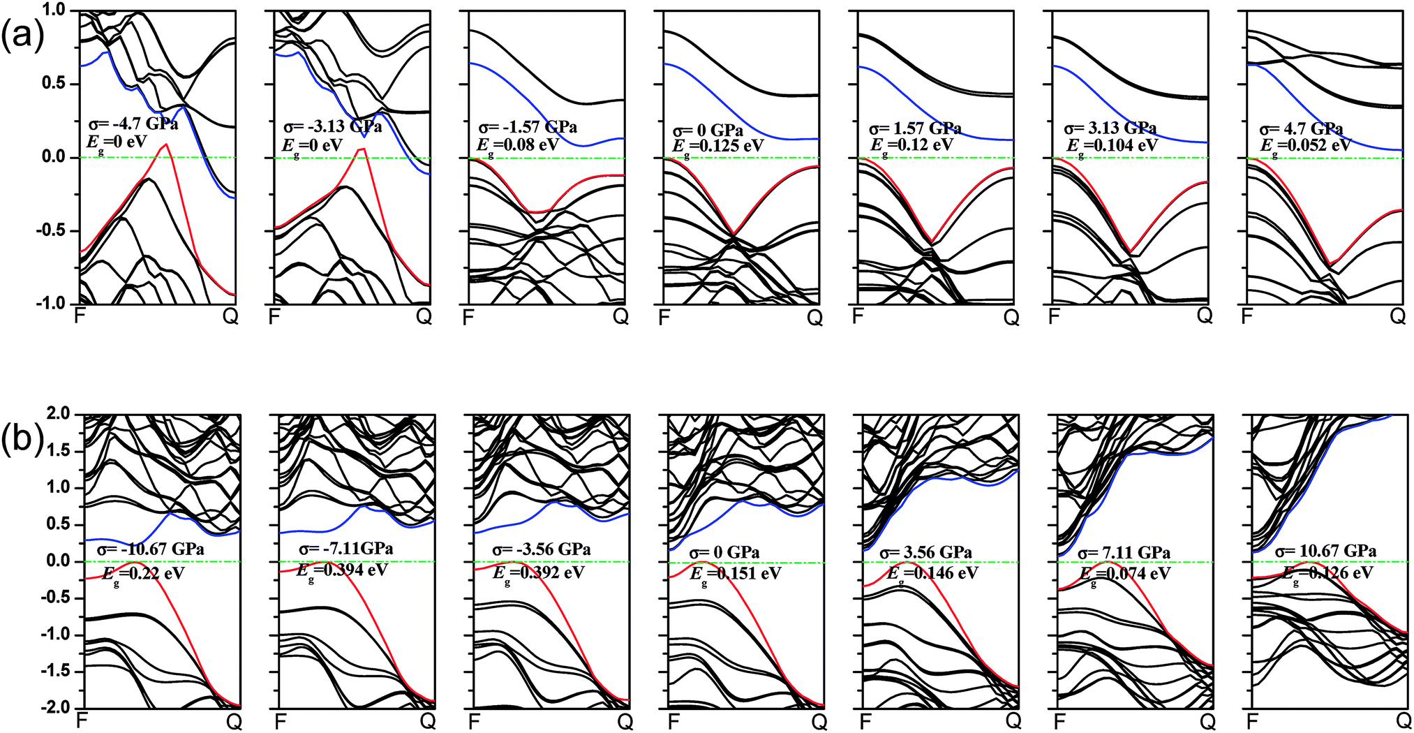
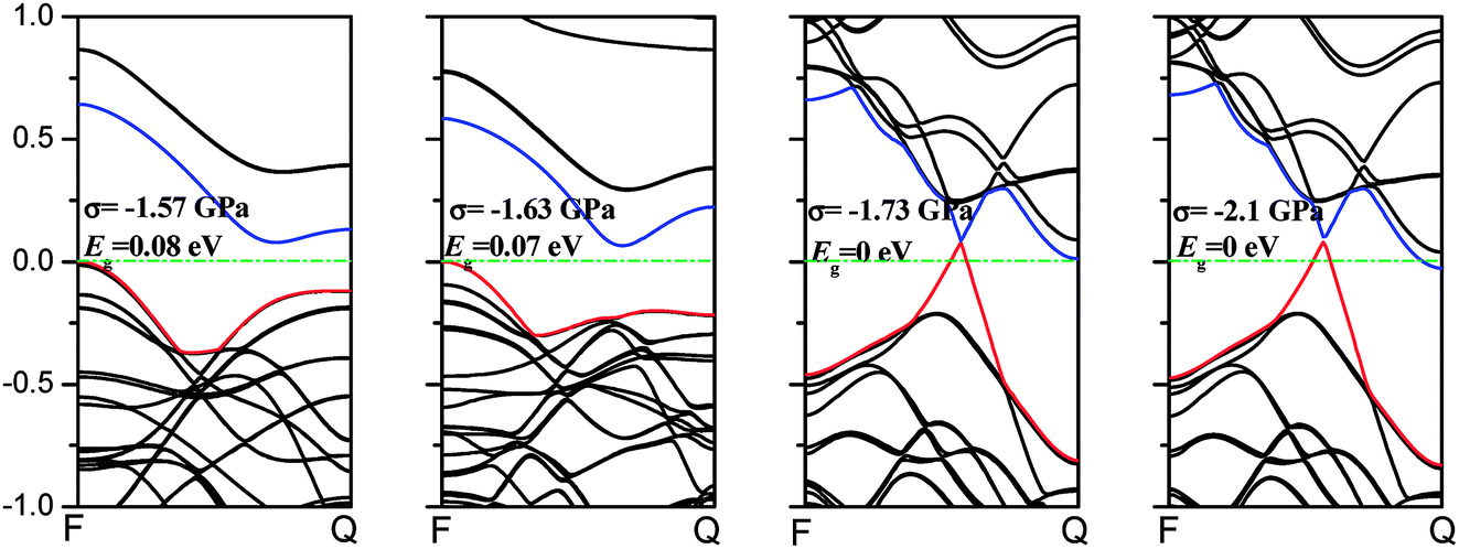
Phosphorene nanotubes. Fig. 7(a) describes the band structure of the zigzag (12.0) nanotubes when the uniaxial stress is added. The band gap of the zigzag (12.0) nanotube is about 0.125 eV and it is close to the result (0.14 eV and 0.31 eV) calculated from the zigzag (14.0) and (16.0) nanotubes.34 The zigzag (12.0) nanotubes exhibit metallic properties when the compression of −4.7 GPa or −3.13 GPa is applied. We also find that when nanotubes turn to a semiconductor, the VBM always remains at F point. At the same time, the CBM shifts from F to Q and decreases with the tension increasing. The zigzag (12.0) nanotube shows an indirect band gap when stress is applied. As shown in Fig. 7(b), the axial stress leads to changes in the band structure in the armchair (0.8) direction. With the stress processing during the test, the position of VBM remains unchanged. As the compression of −10.67 GPa is applied, the armchair nanotubes show a direct band gap. However, when the compression decreases, the CBM moves toward F and nanotubes turn to an indirect band gap.
 |
| | Fig. 7 (a) The band structure of the zigzag phosphorene nanotube along F → Q direction (when the stress is applied along the armchair direction). (b) The band structure of the armchair phosphorene nanotube (when the zigzag-direction stress is added). The green dash lines describe the Fermi level. The blue lines represent the minimum conduction-band states, while the red lines show the maximum valence-band states. | |
Comparison. In this section, we conclude that the applied strain will affect the band structure irrespective of whether in nanosheets or nanotubes. The main role of the strain is to form a new VBM or CBM. Moreover, the new formed VBM or CBM will make phosphorene turn from a direct gap to an indirect one or change from a semiconductor to a metal. Among them, we find that the metallic transition in both nanosheets and nanotubes has some common characteristics. First, the metallic transition in nanosheets and nanotubes is only induced by compression (as shown in Fig. 6 and 7). Second, the compression, which may lead to that transition, is applied only along the armchair direction in nanosheets and the axial direction of the zigzag nanotube. Structurally, the armchair direction in nanosheets is the same as the axial direction of the zigzag nanotubes. The metallic transition in the zigzag nanotubes under the compression is presented in Fig. 8.
 |
| | Fig. 8 Metallic transitions in the zigzag nanotube under the compression. The green dash lines describe the Fermi level. The blue lines represent the minimum conduction-band states, while the red lines show the maximum valence-band states. | |
3.3 Charge carriers
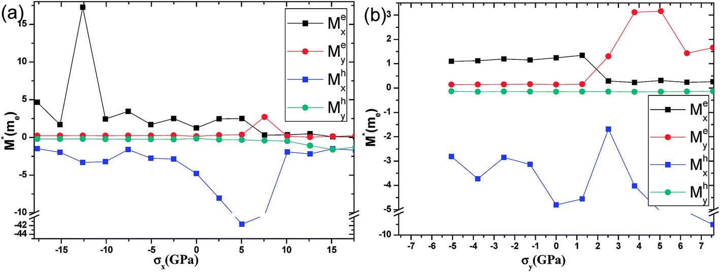
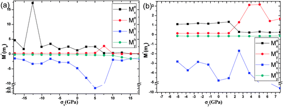
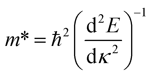
The effective masses of the electron or the hole in phosphorene nanosheets and nanotubes are presented in Fig. 9 and 10. They are calculated according to the formula 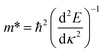 from the band structure. For unstrained phosphorene nanosheets, the calculated effective mass of the electron is 1.244 me in the zigzag direction and 0.146 me in the armchair direction. The effective mass of the hole is −4.8 me in the zigzag direction and −0.148 me in the armchair direction. These results are in good agreement with other theoretical studies.18,19
 |
| | Fig. 9 The electron/hole effective mass according to the (a) x- and (b) y-direction stress. The black line and the red line respectively represent the effective mass of the electron along the zigzag (Mex) and armchair directions (Mey). The blue line represents the effective mass of the hole along the zigzag direction (Mhx) and the green line represents the effective mass of the hole along the armchair direction (Mhy). | |
 |
| | Fig. 10 (a) The electron or hole effective mass in the zigzag (12.0) nanotube along the tube-axis direction. (b) The electron or hole effective mass of the armchair (0.8) nanotube along the tube-axis direction. The stress or compression is added along the tube-axis direction. | |
Phosphorene nanosheets. Fig. 9(a) describes the changes in the effective mass resulting from the zigzag-direction stress. When compression is applied, Mex increases with a slight fluctuation. It peaks at 17.25 me as the compression of −12.61 GPa is applied. The axial tensile stress makes Mex decrease from 2.5 me to 0.3 me at 5.05–7.57 GPa. Interestingly, Mey remains at 0.2 me when compression in the range of −17.66–0 GPa is applied. However, under tensile stress, Mey remains at 0.3 me within the tensile stress range of 0–5.05 GPa, increases to 2.7 me at 7.57 GPa, and finally remains stable at 0.2 me until breakage. The effective mass of the hole along the zigzag direction (Mhx) has a slight fluctuation when zigzag-direction compresses are applied. The average of Mhx is about −2.75 me. With the increase in the tensile stress, Mhx first increases from −4.8 me to −41.7 me at 0–5.05 GPa, decreases sharply from −41.7 me to −1.9 me at 5.05–10.1 GPa, and finally stays at 1.8 me until breakage. In contrast, the effective mass of the hole along the armchair direction (Mhy) remains at −0.27 me when a stress of −17.66–10.1 GPa is applied. Mhy increases slightly from −0.48 me to −1.6 me at the tensile stress range of 10.1–17.66 GPa. Fig. 9(b) presents the effective mass changes with the armchair-direction stress. It should be noted that, when compression is applied, the effective masses of the electron along the zigzag direction (Mex), the electron along the armchair direction (Mey), and the hole along the armchair direction (Mhy) are stabilised at 1.2 me, 0.15 me, and −0.15 me, respectively. However, the effective mass of the hole along the zigzag direction (Mhx) has a large value and a large fluctuation. We also find that Mex decreases from 1.3 me to 0.3 me when the tensile stress increases from 1.26 GPa to 2.52 GPa. In contrast, under the same conditions, Mey may increase from 0.16 me to 1.3 me. After the calculation, we concluded the following. First, the stress along both zigzag and armchair directions has a small effect on Mhy. The value of Mhy will remain stable at −0.27 me. Furthermore, the results also show that Mex, Mey and Mhy are independent of compression along the armchair direction. Second, Mex, Mey and Mhx are very sensitive to tensile stress. The value of Mhx is large and the changes are in a disorder fashion. Mex and Mey change in a contrast way when the system bears the armchair-direction tensile stress. It indicates the conducting anisotropy in phosphorene.
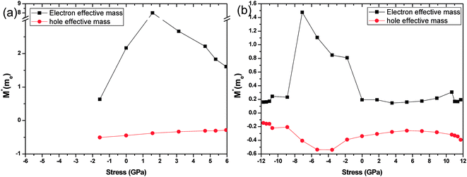
Phosphorene nanotubes. Fig. 10 presents the effective mass along the tube-axis when nanotubes are tested under different stress levels. As shown in Fig. 10(a), the effective mass of the hole that belongs to the zigzag (12.0) nanotube remains stable at −0.37 me. On the contrary, the effective mass of the electron has a large fluctuation. It increases from 0.63 me to 8.00 me at −1.57–1.57 GPa and decreases to 1.61 me until breakage. For the armchair (0.8) nanotube, the effective mass is presented in Fig. 10(b). It shows that the effective masses of the electron and the hole have the same fluctuation area. The electron effective mass increases from 0.23 me to 1.48 me at −8.9–7.11 GPa and then decreases to 0.19 me at −7.11–0 GPa. For the hole effective mass, it increases from −0.21 me to 0.54 me at −8.9–7.11 GPa and then decreases to 0.34 me at −7.11–0 GPa. We find that the strain has little influence on the free holes in nanotubes. For the armchair nanotube, the free electrons show small-scale changes when strain is applied.The strain induced charge carriers vary differently in phosphorene nanosheets and nanotubes. The hole effective mass along the zigzag direction in nanosheets experiences a large fluctuation when strain is applied. Moreover, the free electron will be affected by the tensile stress. Thus, the conducting properties will be largely affected by the applied strain. On the contrary, the free holes in nanotube show independence in the applied strain. The free electrons in the armchair nanotube change a little when strain is applied. It means the nanotubes, particularly the armchair tubes, show a better stability in carriers transport when uniaxial strain is applied.
4. Conclusion
The mechanical behavior of phosphorene nanosheets and nanotubes has been calculated with the first-principles method. The results show that monolayer phosphorene is able to withstand a tensile stress up to 17.66 GPa in the zigzag direction and 7.56 GPa in the armchair direction. The maximum strain along the zigzag direction is about 27%, which is almost the same as that (25%) along the armchair direction. According to the calculation, phosphorene sheets and nanotubes exhibit a super flexibility with a small Young's modulus. In addition, the nanosheet is calculated to have different Young's modulus along different directions. Compared with that of nanosheets, the maximum tensile stress of nanotubes decreases. It indicates that the tensile modulus will decrease with the tensile strain increasing, while the compression modulus increases with increasing compression. The zigzag-direction stress affects the covalent bonds largely, while the armchair-direction stress influences lone-pair electrons remarkably. For nanosheets, the band gap increases with a decrease in compression and decrease with an increase in tensile stress. For nanotubes, the changes in the band gap are in a disordered fashion. Nanotubes hold a narrower band gap compared with nanosheets. The zigzag (12.0) nanotube exhibits metallicity when small compressions are applied. The metallic transition in nanosheets and nanotubes is only induced by the armchair-direction compression. The CBM and VBM shift their positions when stress is applied. For nanosheets, Mex and Mey change in a contrast way under tensile stress. The effective mass of the electron in the zigzag (12.0) nanotube is mainly affected by stress. The free electrons in the armchair nanotube change a little when strain is applied. It means that the nanotubes, particularly the armchair tubes, show a better stability in carriers transport when uniaxial strain is applied.
Conflicts of interest
The authors have declared no conflict of interest.
Acknowledgements
The financial support from the National Natural Science Foundation of China (No. 21376199 and 51002128), the Scientific Research Foundation of Hunan Provincial Education Department (No. 17A205 and 15B235), and the Postgraduate Innovation Foundation of Hunan Province (No. CX2017B308) is greatly acknowledged. This work was also supported by the open project program of Key Laboratory of Intelligent Computing & Information Processing of Ministry of Education.
References
- L. Li, Y. Yu, G. J. Ye, Q. Ge, X. Ou, H. Wu, D. Feng, X. H. Chen and Y. Zhang, Nat. Nanotechnol., 2014, 9, 372–377 CrossRef CAS PubMed.
- S. P. Koenig, R. A. Doganov, H. Schmidt, A. H. Castro Neto and B. Ozyilmaz, Appl. Phys. Lett., 2014, 104, 10451 CrossRef.
- A. Castellanosgomez, L. Vicarelli, E. Prada, J. O. Island, K. L. Narasimhaacharya, S. I. Blanter, D. J. Groenendijk, M. Buscema, G. A. Steele and J. V. Alvarez, 2D Mater., 2014, 1, 025001 CrossRef.
- H. Liu, A. T. Neal, Z. Zhu, Z. Luo, X. Xu, D. Tománek and P. D. Ye, ACS Nano, 2014, 8, 4033–4041 CrossRef CAS PubMed.
- A. Castellanosgomez, J. Phys. Chem. Lett., 2015, 6, 4280–4291 CrossRef CAS PubMed.
- P. W. Bridgman, J. Am. Chem. Soc., 1914, 36, 1344–1363 CrossRef CAS.
- L. Li, Y. Yu, G. J. Ye, X. H. Chen and Y. Zhang, APS March Meeting Abstracts, 2013 Search PubMed.
- F. Xia, H. Wang and Y. Jia, Nat. Commun., 2014, 5, 4458 CAS.
- H. O. H. Churchill and P. Jarilloherrero, Nat. Nanotechnol., 2014, 9, 330–331 CrossRef CAS PubMed.
- A. Carvalho, M. Wang, X. Zhu, A. S. Rodin, H. Su and A. H. C. Neto, Nat. Rev. Mater., 2016, 1, 16061 CrossRef CAS.
- Z. Guo, H. Zhang, S. Lu, Z. Wang, S. Tang, J. Shao, Z. Sun, H. Xie, H. Wang and X. F. Yu, Adv. Funct. Mater., 2015, 25, 6996–7002 CrossRef CAS.
- S. Bertolazzi, J. Brivio and A. Kis, ACS Nano, 2011, 5, 9703–9709 CrossRef CAS PubMed.
- C. Lee, X. Wei, J. W. Kysar and J. Hone, Science, 2008, 321, 385–388 CrossRef CAS PubMed.
- Z. Zhang, Y. Yang, E. S. Penev and B. I. Yakobson, Adv. Funct. Mater., 2016, 27, 1605059 CrossRef.
- Q. Wei and X. Peng, Appl. Phys. Lett., 2014, 104, 372–398 Search PubMed.
- Y. Wang, C. Cong, W. Yang, J. Shang, N. Peimyoo, Y. Chen, J. Kang, J. Wang, W. Huang and T. Yu, Nano Res., 2015, 8, 2562–2572 CrossRef CAS.
- X. Zhang, Z. Lai, C. Tan and H. Zhang, Angew. Chem., Int. Ed., 2016, 55, 8816–8838 CrossRef CAS PubMed.
- X. Peng, Q. Wei and A. Copple, Phys. Rev. B: Condens. Matter Mater. Phys., 2014, 90, 085402 CrossRef.
- R. Fei and L. Yang, Nano Lett., 2014, 14, 2884–2889 CrossRef CAS PubMed.
- A. Brown and S. Rundqvist, Acta Crystallogr., 1965, 19, 684–685 CrossRef CAS.
- M. Elahi, K. Khaliji, S. M. Tabatabaei, M. Pourfath and R. Asgari, Phys. Rev. B: Condens. Matter Mater. Phys., 2015, 91, 115412 CrossRef.
- Y. Kôzuki, Y. Hanayama, M. Kimura, T. Nishitake and S. Endo, J.
Phys. Soc. Jpn., 2007, 60, 1612 CrossRef.
- L. Cartz, S. R. Srinivasa, R. J. Riedner, J. D. Jorgensen and T. G. Worlton, J. Chem. Phys., 1979, 71, 1718–1721 CrossRef CAS.
- V. Tran, R. Soklaski, Y. Liang and L. Yang, Phys. Rev. B: Condens. Matter Mater. Phys., 2014, 89, 817–824 Search PubMed.
- J. Yang, R. Xu, J. Pei, W. M. Ye, F. Wang, Z. Wang, S. Zhang, Z. Yu and Y. Lu, Light: Sci. Appl., 2015, 4, e312 CrossRef CAS.
- W. Zhang, F. Li and J. Hu, et al., J. Phys.: Condens. Matter, 2017, 29, 465501 CrossRef PubMed.
- X. Liao, F. Hao, H. Xiao and X. Chen, Nanotechnology, 2016, 27, 215701 CrossRef PubMed.
- R. Ansari, A. Shahnazari and S. Rouhi, Phys. E, 2017, 88, 272–278 CrossRef CAS.
- H. Guo, N. Lu, J. Dai, X. Wu and X. C. Zeng, J. Phys. Chem. C, 2014, 118, 14051–14059 CAS.
- V. Verma, V. K. Jindal and K. Dharamvir, Nanotechnology, 2007, 18, 435711 CrossRef.
- L. Song, L. Ci, H. Lu, P. B. Sorokin, C. Jin, J. Ni, A. G. Kvashnin, D. G. Kvashnin, J. Lou and B. I. Yakobson, Nano Lett., 2010, 10, 3209–3215 CrossRef CAS PubMed.
- A. Castellanos-Gomez, M. Poot, G. A. Steele, V. D. Z. Hs, N. Agraït and G. Rubio-Bollinger, Adv. Mater., 2012, 24, 772–775 CrossRef CAS PubMed.
- W. Li, G. Zhang and M. Guo, et al., Nano Res., 2014, 7, 518–527 CrossRef CAS.
- T. Hu, A. Hashmi and J. Hong, Nanotechnology, 2015, 26, 415702 CrossRef PubMed.
|
| This journal is © The Royal Society of Chemistry 2017 |
Click here to see how this site uses Cookies. View our privacy policy here. 
 Open Access Article
 This Open Access Article is licensed under a Creative Commons Attribution-Non Commercial 3.0 Unported Licence
 *abc
*abc

 , where S is the XY plane area of the cell, ROD and RID represent the outer and inner radius of a nanotube, respectively, and d is the layered thickness of phosphorene.
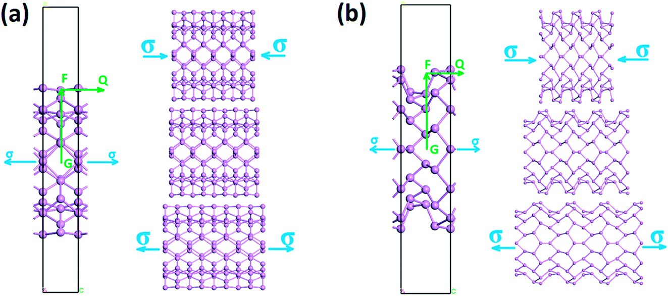

 from the band structure. For unstrained phosphorene nanosheets, the calculated effective mass of the electron is 1.244 me in the zigzag direction and 0.146 me in the armchair direction. The effective mass of the hole is −4.8 me in the zigzag direction and −0.148 me in the armchair direction. These results are in good agreement with other theoretical studies.18,19