
 Open Access Article
 This Open Access Article is licensed under a Creative Commons Attribution-Non Commercial 3.0 Unported Licence
Exposure enhanced photoluminescence of CdS0.9Se0.1 quantum dots embedded in spin-coated Ge25S75 thin films
Stanislav Slang†
 a,
Liudmila Loghina†a,
Karel Palka*ab and
Miroslav Vlceka
a,
Liudmila Loghina†a,
Karel Palka*ab and
Miroslav Vlceka
aCenter of Materials and Nanotechnologies, Faculty of Chemical Technology, University of Pardubice, Pardubice 53210, Czech Republic. E-mail: karel.palka@upce.cz
bDepartment of General and Inorganic Chemistry, Faculty of Chemical Technology, University of Pardubice, Pardubice 53210, Czech Republic
First published on 22nd November 2017
Abstract
Semiconductor quantum dots (QDs) are well known photoluminescent materials. Their potential practical applications depend on their physico-chemical and luminescent properties and also on the properties of hosting material. To ensure that QDs retain their photoluminescence during the preparation of a suitable solid composite form, the solution based casting techniques with deposition at lower temperatures are usually used. In our work, we have doped an inorganic Ge25S75 chalcogenide glass matrix with synthesized CdS0.9Se0.1 QDs and prepared thin films by the solution based spin-coating technique. In comparison with commonly used polymers the Ge25S75 chalcogenide glass thin films a possess high refractive index and wide VIS-NIR-MIR optical transparent region. We also report on the phenomenon of significant UV exposure induced increase of doped thin film photoluminescence intensity which can be exploited in local photo-induced photoluminescence enhancement of doped chalcogenide glass thin films.
Introduction
Semiconductor quantum dots (QDs) have attracted a great deal of interest due to their unique properties.1–4 QDs exhibit size-dependent characteristics and they often possess novel electronic, magnetic, optical, chemical, and mechanical properties that cannot be obtained from their bulk counterparts.5,6 QDs with careful functionalization have been widely used for imaging and sensing7 or tracking particles and cells8 in biology and medicine. Blue- and green-light emitting QDs with high photoluminescent quantum yield (PL QY) and pure emission color are critical elements for the application of solid state light emitting diodes (LEDs) and lasers.9 For this broad class of applications, the Cd-based chalcogenide (this term generally refers to sulfur, selenium and tellurium) QDs are regarded to be promising materials.In the past two decades, significant progress has been made in synthesis of QDs with uniform size, high PL QYs and narrow emission spectra.10,11 Optimization of QDs synthesis was carried out by systematic changing the reaction conditions including the effect of type of solvent,12 form of surfactant,13 precursor form14 and reaction temperature15 in order to increase the QY and monodispersity.
Completely different group of chalcogenides are amorphous chalcogenide glasses (ChGs). They are semiconductors with high refractive index and wide IR transparency window.16–20 ChGs are frequently used in form of bulk glasses (IR optical elements such as lenses, windows etc.)16,17,21 or their amorphous thin films (optical recording discs, diffractive optical elements, planar waveguides, high resolution photoresists, etc.).16–20 Metastability of ChGs often results in their sensitivity to various types of irradiation.16,17,22,23 ChG thin films are usually deposited by physical vapor deposition techniques (e.g. vacuum thermal evaporation, laser ablation, etc.).16–20 Alternatively, ChGs thin films can be also deposited by solution based deposition techniques, which exploits the solubility of ChGs in volatile organic amines.24–27 Laboratory scale deposition techniques (such as spin-coating or dip-coating) have been proven suitable for basic material research.24–27 ChGs thin films were also successfully deposited from their solutions by electrospray28 or spiral bar-coating29 techniques which opens the possibility for their potential mass production by other coating techniques without the need for high vacuum equipment (contrary to the physical vapor deposition methods). The major disadvantage of ChG thin films deposited from solutions is organic residuals content, which can be limiting for some IR optical applications. However, organic residuals content can be significantly reduced by proper post-deposition thermal treatment.30,31
Organic polymers are typically used as a host matrix for PL QDs.32–34 Previous results proved that spin-coated ChG thin films can be also used as host matrix for QDs.35,36 The usage of ChG host matrix can be advantageous because ChGs possess higher refractive index and wider VIS-NIR-MIR transparent region in comparison with organic polymers.37–39 In this work, we report on (a) “one pot” preparation and characterization of highly PL CdS0.9Se0.1 nanoparticles (b) and their usage for doping of Ge25S75 ChG solution. The Ge25S75 ChG is non-toxic40 and the thin films were successfully deposited by spin-coating technique only recently.31 The doped Ge25S75 thin films deposited by spin-coating technique were of good optical quality, well transparent in VIS and NIR and maintained PL of the QDs. The structural changes in structure of doped spin-coated thin films were induced by UV lamp light exposure. Significant enhancement of thin films PL intensity was observed after illumination and we have also proposed possible mechanism of this phenomenon.
Experimental
Synthesis and isolation of CdS0.9Se0.1 nanoparticles
The CdS0.9Se0.1 crystalline quantum dots (QDs) were synthetized using cadmium oxide (CdO 99.99%, Sigma Aldrich), selenium (Se 99.999%, abcr GmbH & Co. KG), sulfur (S 99.999%, Sigma Aldrich), trioctylphosphine (TOP, 97%, Sigma Aldrich), 1-octadecene (ODE, 90%, Sigma Aldrich) and oleic acid (OA, 90%, Sigma Aldrich) precursors. The n-hexane, methanol, toluene, chloroform and acetone solvents (Fisher Scientific) were used for isolation and purification of prepared nanoparticles. Air and/or moisture sensitive chemicals were handled in Ar atmosphere. The reactions were carried out in a standard Schlenk line apparatus under inert Ar atmosphere as well.The S precursor solution (1 M), containing 0.32 g of S, 5 mL of TOP and 5 mL of ODE, was prepared under an Ar atmosphere; the solution was permanently stirred at 50 °C until complete dissolution of S. The Se precursor solution (1 M), containing 0.79 g of Se, 5 mL of TOP and 5 mL of ODE, was prepared under an Ar atmosphere at 100 °C and permanent stirring.
CdS0.9Se0.1 QDs were synthesized using a hot-injection method based on the CdSe synthesis developed by Cooper et al.41 This method was modified according to the synthesized composition. In a 50 mL Schlenk flask 0.385 g CdO (0.003 mol) was suspended with 3.56 mL OA (0.012 mol) in 15 mL ODE. Using a Schlenk line and vacuum pump, the mixture was degassed at room temperature for 20 min, then at 100 °C 20 min and then finally heated up to 280 °C to form clear solution. The mixture of S (2.7 mL, 0.0027 mol of S) and Se (0.3 mL, 0.0003 mol of Se) precursor solutions was injected instantaneously into the heated CdO solution using an air free injection procedure. After injection, the temperature of reaction mixture was decreased to 240 °C and kept at this temperature for growing of QDs. The size of QDs was monitored using UV-VIS spectroscopy and photoluminescence (PL) measurements by taking out of aliquots at different time intervals. The aliquots were dispersed in toluene for spectroscopic measurements.
The crude reaction mixture was dissolved in 50 mL of n-hexane and washed three times with methanol to remove unreacted precursors. The hexane solution was diluted by 50 mL of chloroform. Finally, the QDs were precipitated by adding anhydrous acetone. Precipitated QDs were separated in a centrifuge (Gusto Mini Centrifuge, Fisherbrand) by spinning down at 10![[thin space (1/6-em)]](https://www.rsc.org/images/entities/char_2009.gif) 000 rpm for 7 min. For purification of QDs this procedure was repeated 3 times. Separated pure QDs were dried in vacuum for 4 hours. The weight of pure CdS0.9Se0.1 QDs was 0.521 g.
000 rpm for 7 min. For purification of QDs this procedure was repeated 3 times. Separated pure QDs were dried in vacuum for 4 hours. The weight of pure CdS0.9Se0.1 QDs was 0.521 g.
The UV-VIS absorbance spectra of prepared aliquot QDs solutions in toluene were measured using UV-VIS-NIR optical spectrometer Shimadzu UV3600 (Shimadzu) in spectral region 330–650 nm. The PL measurements were performed using PTI QuantaMaster 400 (Horiba) steady state spectrofluorometer in spectral range 390–700 nm using excitation wavelength λ = 375 nm. X-ray diffraction measurements (XRD) of dried QDs were performed using Bruker D8 advance Diffractometer with Cu-Kα radiation. Data were recorded across a 2θ range of 20–65° with a step size of 0.05°.
In order to verify the shape and diameter of prepared QDs, the particles were deposited onto carbon hole membrane copper grid and HR-TEM images were taken on a FEI Titan Themis 60 (FEI) high resolution transmission electron microscope at acceleration voltage 300 kV.
Deposition and characterization of doped Ge25S75 thin films
The source Ge25S75 bulk glass was synthetized using standard melt-quenching method. High purity 5 N elements were loaded into the quartz ampule in appropriate amounts and sealed under vacuum (∼10−3 Pa). The glass synthesis was performed in rocking tube furnace at 950 °C for 72 hours. The ampule with melted glass was quenched in cold water.Prepared Ge25S75 bulk glass was powdered in agate bowl and dissolved in n-butylamine solvent (BA) with concentration 0.0804 g of glass powder per 1 mL of BA. The vacuum dried CdS0.9Se0.1 QDs were dispersed in chloroform with concentration 0.02 g of QDs per 1 mL of chloroform. The 1.4 mL of Ge25S75 glass solution was mixed with 0.1 mL of QDs solution right before thin film deposition (0.075 g Ge25S75 and 0.0013 g CdS0.9Se0.1 QDs per 1 mL of final solution). Prepared solution of Ge25S75 ChG and CdS0.9Se0.1 QDs was clear without any precipitate. The blank (undoped) glass solution was prepared by mixing 1.4 mL of Ge25S75 glass solution with 0.1 mL of pure chloroform. Doped and undoped ChG thin films were deposited using spin-coating method on spin-coater SC110 (Best Tools) by pipetting 100 μL of solution onto soda-lime glass substrates rotating at 2000 rpm yielding thin films of good optical quality. The thin films were stabilized by annealing at 60 °C for 20 minutes on a hot plate immediately after deposition (hereinafter referred as as-prepared thin films). Deposited samples were stored in dry and dark environment.
Samples of as-prepared thin films were annealed at temperatures 90, 120, 150, 180 and 210 °C for 60 min on precise annealing table (Conbrio) inside argon filled annealing chamber. In order to examine the effect of irradiation on doped spin-coated thin films the samples were exposed to UV lamp light (365 nm, 137 mW cm−2) in argon atmosphere for 60 min.
Transmission spectra of studied thin films were measured using UV-VIS-NIR optical spectrometer (Shimadzu UV3600) in spectral region 190–2000 nm. The spectra measurements were always performed on four samples with the same treatment. The elemental compositions of the as-prepared, annealed and exposed thin films together with vacuum dried CdS0.9Se0.1 QDs were analyzed by energy dispersive X-ray microanalysis method (EDS) using scanning electron microscope (LYRA 3, Tescan, Czech Republic) equipped with EDS analyzer Aztec X-Max 20 (Oxford Instruments) at acceleration voltage 5 kV. The PL measurements of doped thin films were performed using QuantaMaster 400 steady state spectrofluorometer in spectral range 410–620 nm using excitation wavelength λ = 400 nm (5 nm slit), which was not absorbed by Ge25S75 thin film matrix.
Results and discussion
Crystallographic structure of vacuum dried CdS0.9Se0.1 QDs powder was determined by XRD (Fig. 1). All measured diffractions can be assigned to the standard pattern of the face centered cubic phase with space group![[F with combining macron]](https://www.rsc.org/images/entities/i_char_0046_0304.gif) 43m, which suggests previously proposed mechanism of low temperature crystal growth.42–44 Calculated cell parameter a of studied QDs is 5.878(4) Å. The low width of observed diffraction peaks suggests nanosize QDs. The mean crystalline domain size D of CdS0.9Se0.1 QDs was calculated using Scherrer equation:45
43m, which suggests previously proposed mechanism of low temperature crystal growth.42–44 Calculated cell parameter a of studied QDs is 5.878(4) Å. The low width of observed diffraction peaks suggests nanosize QDs. The mean crystalline domain size D of CdS0.9Se0.1 QDs was calculated using Scherrer equation:45| D = (Kλ)/(βcosθ) |
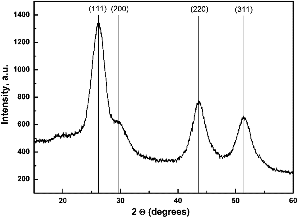 | ||
| Fig. 1 XRD pattern of CdS0.9Se0.1 crystalline nanoparticles. | ||
The HR-TEM microscope was used to study the shape and diameter of prepared CdS0.9Se0.1 QDs. Measured TEM scans (Fig. 2) confirm that QDs have spherical shape and narrow size distribution. Using the image analysis method, the average QDs size was determined at 3.98 ± 0.39 nm. The difference from QDs diameter obtained by Scherrer formula (2.93 nm) can be attributed to model's neglection of surface effects which starts to be more eminent in nano-diameters. The well-developed lattice fringes (inset of Fig. 2) indicate a good crystallinity of studied CdS0.9Se0.1 QDs sample.
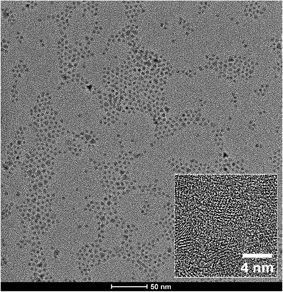 | ||
| Fig. 2 The HR-TEM image of CdS0.9Se0.1 crystalline nanoparticles. | ||
The elemental composition of prepared QDs powder was studied by EDS technique. The results confirmed Cd54.4S39.9Se5.7 QDs composition, which slightly differs from planned Cd50S45Se5 (∼CdS0.9Se0.1) composition probably due to different reactivity of used precursors.46–48 The EDS spectra also confirmed the presence of carbon and oxygen, which can be explained by presence of oleic acid capping shell. The different precursor reactivity can potentially affect the radial distribution of elements within the volume of prepared quantum dots. In our case we cannot exclude the presence of elemental gradient due to the higher reactivity of TOP-Se precursor.47,48
UV-VIS absorption spectra of aliquot QDs samples taken from reaction mixture at various times since the start of reaction are presented in Fig. 3. With increasing reaction time the absorption peak maxima are shifting towards longer wavelengths which can be explained by increasing of QDs size.
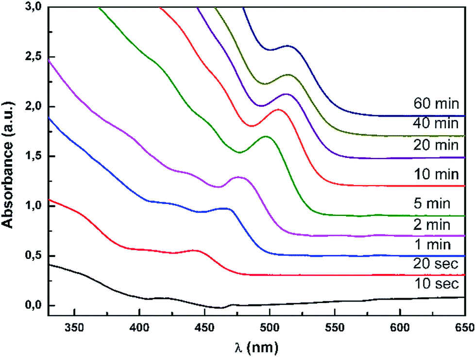 | ||
| Fig. 3 Chronological evolution of absorption spectra of CdS0.9Se0.1 QDs. | ||
Accordingly, the position of their photoluminescence (PL) peaks is also shifting towards higher wavelengths (Fig. 4A). The PL peak position is changing from 447 nm for sample taken from reaction mixture at 10 s to 544 nm for samples taken from reaction mixture at 60 min. The reaction time has also high influence on values of PL peak maximal intensity (Fig. 4B).
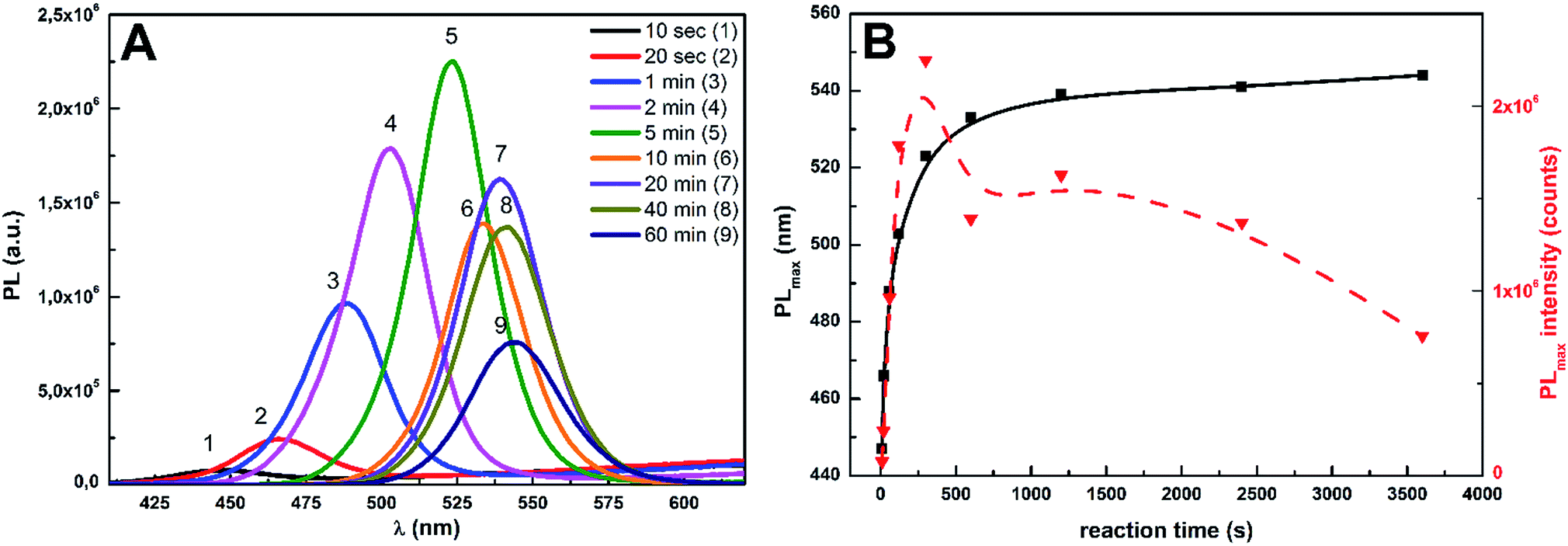 | ||
| Fig. 4 The evolution of photoluminescence (PL) spectra of CdS0.9Se0.1 QDs (A) in dependence on reaction time, dependence of PL maxima position and intensity on reaction time (B). | ||
Their values are significantly increasing up to the reaction time of 5 min. After that, the values of PL intensities are gradually decreasing. The CdS0.9Se0.1 QDs prepared at the reaction time of 60 min were chosen for doping of Ge25S75 chalcogenide thin films, because their PL band position lies well-inside the transparent region of planned Ge25S75 chalcogenide glass matrix.31
It was confirmed that Ge25S75 chalcogenide glass thin films can be prepared from n-butylamine (BA) solution by spin-coating technique in good optical quality.31 For doping of Ge25S75 chalcogenide glass thin films with prepared CdS0.9Se0.1 QDs it is necessary to mix both components without precipitation in mixed solution. Thus, the CdS0.9Se0.1 QDs were dispersed in chloroform whose small addition into BA-Ge25S75 solution did not induced any observable changes in homogeneity.
The PL spectra of CdS0.9Se0.1 QDs (0.005 g mL−1) in various solutions are presented in Fig. 5. The QDs solution in pure chloroform (CHCl3) has the highest PL intensity with peak maximum at 554 nm which is slightly higher that the peak maximum at 544 nm found in toluene aliquot solution (Fig. 4B, 3600 s). Small addition of BA into chloroform QDs solution (0.1 mL of BA into 1.4 mL of QDs chloroform solution) significantly decreased PL intensity. When the same volume of Ge25S75 or S solution in BA (0.03 g mL−1) was mixed with QDs chloroform solution, the PL was practically extinguished. It can be explained by reaction of CdS0.9Se0.1 QDs with BA and/or products of Ge25S75 chalcogenide glass dissolution in BA. The possible reaction of oleic acid capping agent with basic BA also cannot be excluded. The Ge–S and Ge–Sb–S chalcogenide glasses are dissolving in aliphatic amines and forming ionic compounds of alkyl ammonium germanium sulfide (AAGS) salts.26,31 Due to the over-stoichiometry of S in Ge25S75 bulk glass, the BA chalcogenide glass solution also contain free sulfur fragments, which were also found in BA solutions of S-rich As–S chalcogenide glasses.25 Those dissolution products and BA solvent are probably reacting with CdS0.9Se0.1 QDs, which is reflected in decrease of their PL intensity.
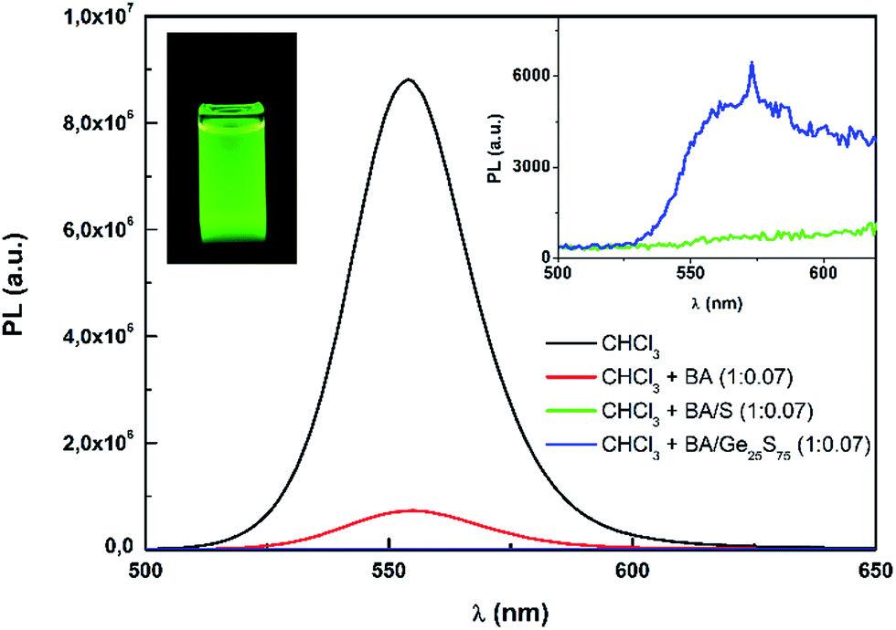 | ||
| Fig. 5 PL spectra of CdS0.9Se0.1 QDs in chloroform (CHCl3) with addition of various solutions. The left inset photo shows the CdS0.9Se0.1 QDs-CHCl3 solution under UV lamp light. | ||
The Ge25S75 solution in BA (1.4 mL) was mixed with CdS0.9Se0.1 QDs solution in chloroform (0.1 mL) to yield the concentration of 0.075 g Ge25S75 and 0.0013 g CdS0.9Se0.1 QDs/mL of final solution. The clear solution without any precipitate was used for spin-coating of doped thin films. To distinguish the effect of chloroform and QDs on properties of deposited thin films, the undoped (blank) thin films were deposited from mixture of Ge25S75 solution in BA (1.4 mL) and pure chloroform (0.1 mL). It was confirmed, that spin-coated chalcogenide glass thin films of various compositions can be also photo-sensitive.30,49,50 Thus, the prepared thin films were also exposed to UV lamp light (365 nm) and the influence of UV exposure on optical properties and PL was studied.
The geometrical and optical parameters of prepared blank and doped Ge25S75 thin films were calculated by procedure presented in29,47 based on Swanepoel's model51 and Wemple–DiDomenico's equation52 from transmission spectra of studied thin films. Due to the size of used QDs (d ∼ 4 nm) which is significantly smaller than probing wavelengths (d ≪ λ) the measured thin films can be considered homogeneous and thus used model of transmission spectra remains valid. The quality of fit was determined as residual sum of squares (RSS) between fitted and experimental spectrum. The RSS of fitted data didn't exceed the value of 0.04 (within fitted transparent region ∼400–2000 nm). Provided data of optical parameters and thickness represent the average values of four measurements and the error bars stand for the standard deviation of calculated values. The typical fitted spectrum of as-prepared and annealed thin film together with Tauc's plot53 are presented in Fig. 6.
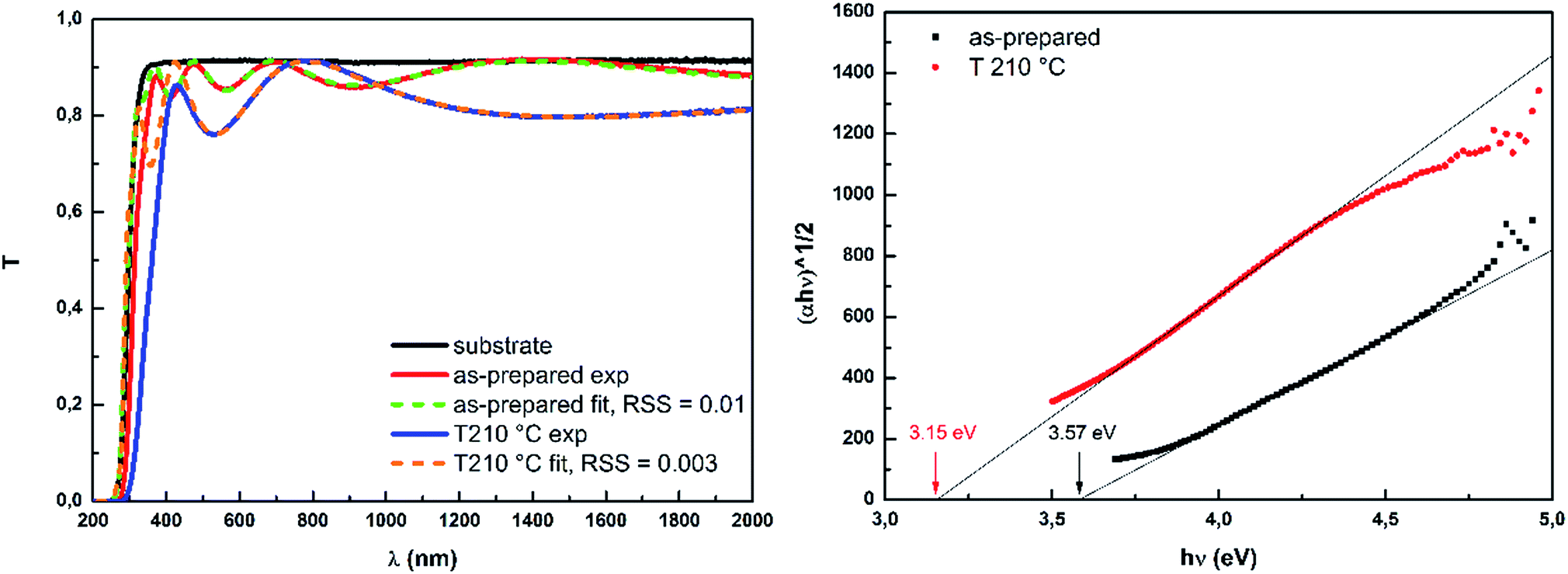 | ||
| Fig. 6 The measured and fitted transmission spectra (left) and Tauc's plots (right) of as-prepared and annealed spin-coated doped Ge25S75 thin films (exp – experimental data, fit – fitted data, RSS – residual sum of squares in fitted transparent region). | ||
Fig. 7 demonstrates that the thicknesses of all studied samples are significantly decreasing with increasing annealing temperature. Thickness decrease can be explained by thermal decomposition of present AAGS salts connected with releasing of organic solvent residuals and ongoing structural polymerization. Previously it was confirmed that these salts start to decompose at ∼120 °C.31 The decomposition process should be practically completed at 210 °C,31 when the Ge25S75 thin film annealed at 210 °C has ∼48% of as-prepared thin film thickness. The data also proves that doping and UV exposure treatment have no significant effect on the thickness of studied thin films.
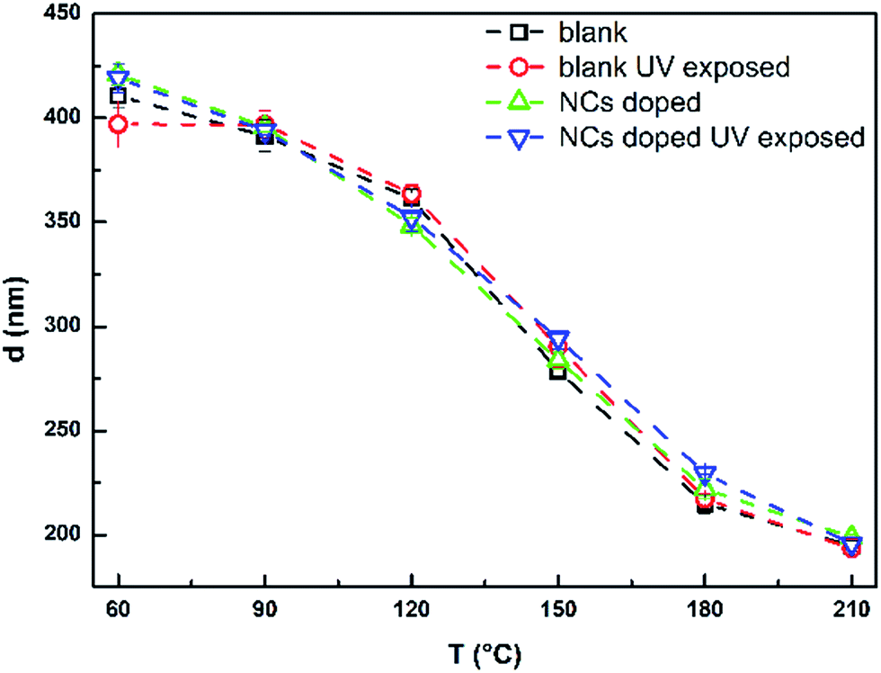 | ||
| Fig. 7 The thickness of studied blank and doped unexposed and UV exposed Ge25S75 thin films in dependence on the annealing temperature. | ||
The refractive index n1550 (λ = 1550 nm) of all studied samples is increasing with increasing annealing temperature (Fig. 8A). The refractive index values of blank and CdS0.9Se0.1 QDs doped unexposed thin films are nearly identical. Data proved that Ge25S75 spin-coated thin films are also photo-sensitive. The refractive index of UV exposed blank and doped thin films annealed at 120 and 150 °C is lower than refractive index of unexposed samples. Values of refractive index of samples annealed at 180 and 210 °C are not influenced by the UV exposure. Thin films annealed above 150 °C are more structurally polymerized and with significantly decreased content of organic residuals.31 Thus, the observed photo-sensitivity is probably connected with organic residuals content and level of structural polymerization.31
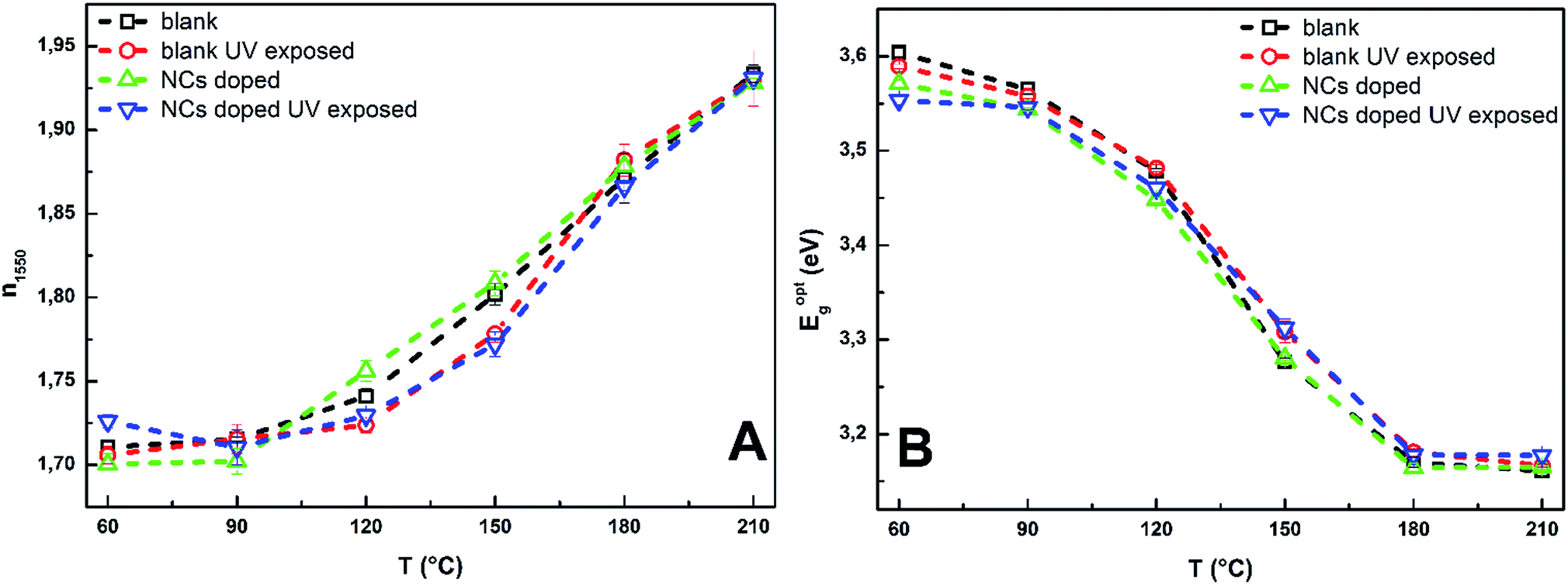 | ||
| Fig. 8 The refractive index n1550 at λ = 1550 nm (A) and optical bandgap Eoptg (B) of studied blank, doped unexposed and UV exposed Ge25S75 thin films in dependence on the annealing temperature. | ||
Contrary to refractive index, the optical bandgap Eoptg of studied thin films is decreasing with increasing annealing temperature – thermo-induced darkening (Fig. 8B). The data proved that UV exposure and doping have no significant effect on Eoptg of studied thin films. The observed differences are within the experimental error of used evaluation method.
The elemental composition of Ge25S75 thin films was studied by EDS analysis. EDS confirmed that as-prepared thin films have composition Ge25.8S74.2, which is within EDS margin of error to that of planned nominal composition Ge25S75. With increasing annealing temperature, some portion of sulfur is released from thin film matrix leaving S depleted Ge27.9S72.1 thin film annealed at 210 °C. The EDS analysis of doped thin films have not confirmed the presence of Cd or Se which would indicate CdS0.9Se0.1 QDs content in thin films matrix. It could be explained by low concentration of QDs, bellow the detection limit of detector (<0.1 at%).
The content of organic residuals in thin film matrix was studied using the content of N atoms. BA molecule contains only one N atom and no other sources of N can be expected. Thus, content of N should be equivalent to content of organic BA residuals. Fig. 9 demonstrates that the content of organic residuals is decreasing with increasing annealing temperature. The shape of obtained curves is similar to the trend of thermal dependent thickness decrease (Fig. 7), which supports the strong connection between thermal induced thickness decrease and releasing of organic residuals from thin film matrix. The doping or UV exposure of studied thin films have no significant effect on the content of organic residuals, with exception of doped sample annealed at 120 °C.
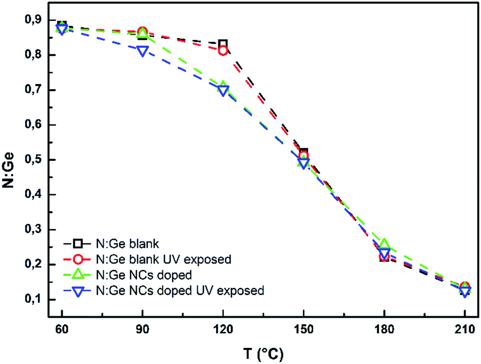 | ||
| Fig. 9 Dependence of nitrogen/germanium ratio measured by EDS on the annealing temperature. | ||
The PL spectra of studied Ge25S75 thin films were recorded using an excitation wavelength 400 nm (∼3.1 eV), which should be transmitted by chalcogenide glass matrix (see Fig. 8B). The PL spectra confirmed that neither unexposed nor exposed blank samples have any significant PL in VIS spectral region (Fig. 10). Contrary, the unexposed doped thin films exhibit PL at 537 nm. The intensity of observed peaks is significantly decreasing with increasing annealing temperature. Previous results confirmed, that thermo-induced structural changes can be expected in Ge25S75 spin-coated thin films.31 With increasing annealing temperature, the glass matrix of Ge–S spin-coated thin film is more compact and polymerized. Present CdS0.9Se0.1 QDs can be also bonded to glass matrix by sulfur bridging atoms, which can result in decrease of QDs PL due to the exciton energy transfer and possible disruption of QDs crystalline lattice. Kovalenko et al.35 have prepared inorganically functionalized core–shell PbS/CdS QDs with As–S capping agent, which had strong IR PL in As2S3 glass matrix. Novak et al.36 have also successfully doped Ge23Sb7S70 glass matrix with PbS quantum dots and core–shell CdSe/ZnS QDs, but they have obtained well-developed and separated PL peaks only by using the core–shell CdSe/ZnS QDs. Thus, the QDs shell is probably bonded to glass matrix during stabilization annealing, leaving the QDs core protected and their annealed doped chalcogenide thin films are well luminescent.
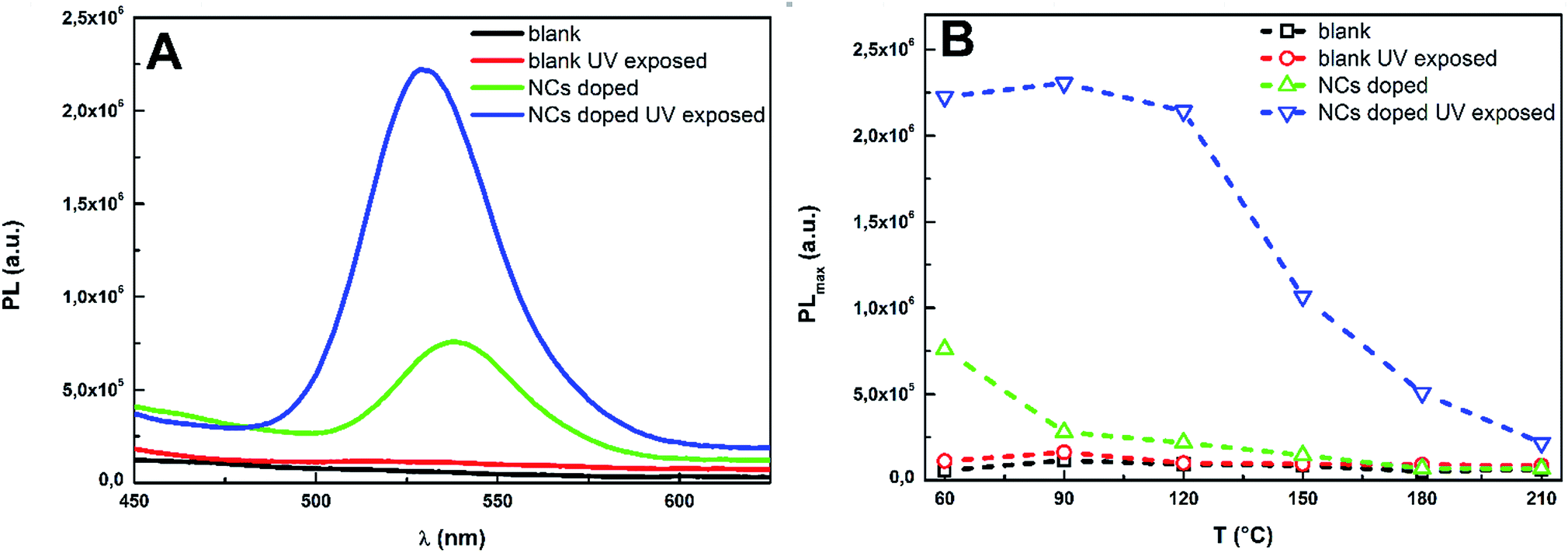 | ||
| Fig. 10 The PL spectra of blank and doped as-prepared Ge25S75 thin films (A) together with PL intensities at PL maxima of treated blank and doped Ge25S75 thin films (B). | ||
The UV exposure of Ge25S75 doped thin film samples has a strong influence on their PL (Fig. 10 and 11). The PL intensity values of UV exposed doped thin films are ∼3–10 times higher than the values of unexposed doped samples PL. The PL maxima are also slightly shifted to shorter wavelength (530 nm) due to the UV exposure. The UV exposure induced enhancement of pure Zn–Ni–S QDs PL was already reported by Z. Jindal and N. K. Verma.54 Their QDs were exposed to hard UV light (255 nm) for 24 hours, which induced changes in QDs structural properties resulting in slight increase in PL intensity. Our Ge25S75 doped thin films were exposed to 365 nm UV light only for 60 min, but increase in PL intensity is much more significant. Considering our results as well as results published in,35,36 we can assume that observed UV induced increase in PL intensity is probably connected with some structural changes on the boundary between CdS0.9Se0.1 QDs and Ge25S75 glass matrix.
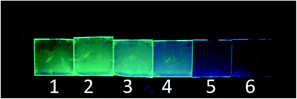 | ||
| Fig. 11 The CdS0.9Se0.1 QDs doped spin-coated Ge25S75 thin films after 60 min UV exposure under UV lamp light. 1 – as-prepared thin film, 2 – annealed at 90 °C, 3 – annealed at 120 °C, 4 – annealed at 150 °C, 5 – annealed at 180 °C, 6 – annealed at 210 °C. | ||
With increasing annealing temperature of pre-exposed thin films, the QDs are more bonded into the structure of chalcogenide glass thin film and the effect of UV exposure is decreased. The effect of UV lamp light exposure which resulted in such significant increase in films' PL intensity can be exploited in local PL enhancement induced by beam of higher energies whereas the beam of lower energy would only induce the PL without changing of PL intensity.
Although the physico-chemical processes in mixed QDs/glass solution and in doped spin-coated thin films during annealing and exposure are relatively complicated issue we propose one possible interpretation of the presented data. As discussed above, after mixing of CdS0.9Se0.1 QDs with Ge25S75 BA solution the QDs are bonding with chalcogenide glass fragments. This process is probably accelerated by substitution of oleic acid capping agent with BA molecules.55 Products of this reaction have no significant PL which can be explained by absence of appropriate protecting QDs shell. After deposition of thin films from prepared solution, the QDs are weakly bonded to as-prepared glass matrix. The structure of thin film and QDs is gradually polymerized with increasing of annealing temperature which further decreases the PL intensity. UV exposure of deposited thin films probably induces releasing of QDs from bonds with glass matrix which significantly increases PL intensity, but the effect of this process depends on thermal pre-history of sample.
Conclusions
The spherical CdS0.9Se0.1 semiconductor quantum dots (QDs) with 3.98 ± 0.39 nm in diameter were synthesized using a hot-injection method. The QDs in toluene exhibit an intensive luminescence with narrow PL peak at 544 nm. Vacuum dried QDs were mixed with Ge25S75 n-butylamine solution and thin films of specular quality were deposited by spin-coating technique. Data proved that the thickness, optical parameters and elemental composition of thin films are not affected by QDs doping. The doped as-prepared thin film exhibit low intensity photoluminescence (PL) with the peak maximum at 537 nm. The PL intensity of doped samples is decreasing with increasing annealing temperature. However, luminescence of doped thin films can be significantly enhanced (3–10 times) by UV light exposure probably due to the photo-induced structural changes on boundary between CdS0.9Se0.1 QDs and Ge25S75 glass matrix. The photo-induced increase of PL intensity can be potentially used for local PL enhancement induced by beam of higher energies whereas the beam of lower energy would only induce the PL without changing of PL intensity.Conflicts of interest
There are no conflicts to declare.Acknowledgements
Authors appreciate financial support from project No. 16-13876S financed by the Grant Agency of the Czech Republic (GA CR) as well as support from the grants LM2015082 and ED4.100/11.0251 from the Ministry of Education, Youth and Sports of the Czech Republic. The TEM measurements were carried out with the support of CEITEC Nano Research Infrastructure (ID LM2015041, MEYS CR, 2016–2019), CEITEC Brno University of Technology. Authors thank to Assoc. Prof. Ludvik Benes (University of Pardubice) for XRD analyses.References
- T. Wakaoka, K. Hirai, K. Murayama, Y. Takano, H. Takagi, S. Furukawa and S. Kitagawa, J. Mater. Chem. C, 2014, 2, 7173–7175 RSC
.
- B. Rajbanshi, S. Sarkar and P. Sarkar, J. Mater. Chem. C, 2014, 2, 8967–8975 RSC
- S. Dey, S. Chen, S. Thota, M. R. Shakil, S. L. Suib and J. Zhao, J. Phys. Chem. C, 2016, 120, 20547–20554 CAS
- A. Marchioro, P. J. Whitham, K. E. Knowles, T. B. Kilburn, P. J. Reid and D. R. Gamelin, J. Phys. Chem. C, 2016, 120, 27040–27049 CAS
- G. G. Yordanov, G. D. Gicheva and C. D. Dushkin, Mater. Chem. Phys., 2009, 113, 507–510 CrossRef CAS
- K. Ersching, C. E. M. Campos, J. C. de Lima and T. A. Grandi, Mater. Chem. Phys., 2008, 112, 745–748 CrossRef CAS
- I. L. Medintz, H. T. Uyeda, E. R. Goldman and H. Mattoussi, Nat. Mater., 2005, 4, 435–446 CrossRef CAS PubMed
- Y. Chang, F. Pinaud, J. Antleman and S. Weiss, J. Biophotonics, 2008, 1, 287–298 CrossRef CAS PubMed
- J. Kwak, W. K. Bae, D. Lee, I. Park, J. Lim, M. Park, H. Cho, H. Woo, D. Y. Yoon, K. Char, S. Lee and C. Lee, Nano Lett., 2012, 12, 2362–2366 CrossRef CAS PubMed
- B. Zhou, L. Tao, Y. H. Tsang and W. Jin, J. Mater. Chem. C, 2013, 1, 4313–4318 RSC
- D. Roy, T. Routh, A. V. Asaithambi, S. Mandal and P. K. Mandal, J. Phys. Chem. C, 2016, 120, 3483–3491 CAS
- S. Sapra, A. L. Rogach and J. Feldmann, J. Mater. Chem., 2006, 16, 3391–3395 RSC
- D. V. Talapin, A. L. Rogach, A. Kornowski, M. Haase and H. Weller, Nano Lett., 2001, 1, 207–211 CrossRef CAS
- J. Hambrock, A. Birkner and R. A. Fischer, J. Mater. Chem., 2001, 11, 3197–3201 RSC
- A. Nag, S. Sapra, S. Chakraborty, S. Basu and D. D. Sarma, J. Nanosci. Nanotechnol., 2007, 7, 1965–1968 CrossRef CAS PubMed
- K. Tanaka and K. Shimakawa, Amorphous Chalcogenide Semiconductors and Related Materials, Springer, New York, 2011 Search PubMed
- Z. Borisova, Glassy Semiconductors, Plenum Press, New York, 1981 Search PubMed
- R. M. Almeida, L. F. Santos, A. Simens, A. Ganjoo and H. Jain, J. Non-Cryst. Solids, 2007, 18–21, 2066–2068 CrossRef
- E. Baudet, C. Cardinaud, A. Girard, E. Rinnert and V. Nazabal, J. Non-Cryst. Solids, 2016, 444, 64–72 CrossRef CAS
- A. Stronski, M. Vlcek and A. Sklenar, Quant. Electron. Optoelectron., 2000, 3, 394–399 CAS
- D. H. Cha, H. Kim, Y. Hwang, J. C. Jeong and J. Kim, Appl. Opt., 2012, 51, 5649–5656 CrossRef CAS PubMed
- T. Kanamori, Y. Terunuma, S. Takahashim and M. Miyashita, J. Lightwave Technol., 1984, 2, 607–613 CrossRef
- K. Tanaka and M. Mikami, Phys. Status Solidi C, 2011, 8, 2756–2760 CrossRef CAS
- G. Chern and I. Lauks, J. Appl. Phys., 1982, 53, 6979–6982 CrossRef CAS
- S. Slang, K. Palka, L. Loghina, A. Kovalskiy, H. Jain and M. Vlcek, J. Non-Cryst. Solids, 2015, 426, 125–131 CrossRef CAS
- M. Waldmann, J. D. Musgraves, K. Richardson and C. B. Arnold, J. Mater. Chem., 2012, 22, 17848–17852 RSC
- L. Strizik, T. Wagner, V. Weissova, J. Oswald, K. Palka, L. Benes, M. Krbal, R. Jambor, C. Koughia and S. Kasap, J. Mater. Chem. C, 2017, 5, 8489–8497 RSC
- S. Novak, D. E. Johnston, C. Li, W. Deng and K. Richardson, Thin Solid Films, 2015, 588, 56–60 CrossRef CAS
- K. Palka, T. Syrovy, S. Schröter, S. Brückner, M. Rothardt and M. Vlcek, Opt. Mater. Express, 2014, 4, 384–395 CrossRef CAS
- S. Slang, K. Palka, H. Jain and M. Vlcek, J. Non-Cryst. Solids, 2017, 457, 135–140 CrossRef CAS
- S. Slang, P. Janicek, K. Palka and M. Vlcek, Opt. Mater. Express, 2016, 6, 1973–1985 CrossRef CAS
- B. O. Dabbousi, M. G. Bawendi, O. Onitsuka and M. F. Rubner, Appl. Phys. Lett., 1995, 66, 1316–1318 CrossRef CAS
- H. Mattoussi, L. H. Radzilowski, B. O. Dabbousi, D. E. Fogg, R. R. Schrock, E. L. Thomas, M. F. Rubner and M. G. Bawendi, J. Appl. Phys., 1999, 86, 4390–4399 CrossRef CAS
- M. Zhu, X. Peng, Z. Wang, Z. Bai, B. Chen, Y. Wang, H. Hao, Z. Shao and H. Zhong, J. Mater. Chem. C, 2014, 2, 10031–10036 RSC
- M. V. Kovalenko, R. D. Schaller, D. Jerzab, M. A. Loi and D. V. Talapin, J. Am. Chem. Soc., 2012, 134, 2457–2460 CrossRef CAS PubMed
- S. Novak, L. Scarpantonio, J. Novak, M. D. Pre, A. Martucci, J. D. Musgraves, N. D. McClenaghan and K. Richardson, Opt. Mater. Express, 2013, 3, 729–738 CrossRef CAS
- N. Sultanova, S. Kasarova and I. Nikolov, Bulg. J. Phys., 2013, 40, 258–264 CAS
- J. Liu and M. Ueda, J. Mater. Chem., 2009, 19, 8907–8919 RSC
- N. Tanio and Y. Koike, Polym. J., 2000, 32, 43–50 CrossRef CAS
- H. Takebe, R. Kitagawa and D. W. Hewak, J. Ceram. Soc. Jpn., 2005, 113, 37–43 CrossRef CAS
- J. K. Cooper, A. M. Franco, S. Gul, C. Corrado and J. Z. Zhang, Langmuir, 2011, 27, 8486–8493 CrossRef CAS PubMed
- Q. Wang, D. C. Pan, S. C. Jiang, X. L. Ji, L. J. An and B. Z. Jiang, Chem.–Eur. J., 2005, 11, 3843–3848 CrossRef CAS PubMed
- C. Unni, D. Philip, S. L. Smitha, K. M. Nissamudeen and K. C. Gopachandran, Spectrochim. Acta, Part A, 2009, 72, 827–832 CrossRef CAS PubMed
- Y. Jun, S. M. Lee, N. J. Kang and J. Cheon, J. Am. Chem. Soc., 2001, 123, 5150–5151 CrossRef CAS PubMed
- B. E. Warren, X-ray Diffraction, Dover Publications, New York, 1990 Search PubMed
- J. Cho, Y. K. Jung and J. Lee, J. Mater. Chem., 2012, 22, 10827–10833 RSC
- T. P. A. Ruberu, H. R. Albright, B. Callis, B. Ward, J. Cisneros, H.-J. Fan and J. Vela, ACS Nano, 2012, 6, 5348–5359 CrossRef CAS PubMed
- J. Vela, J. Phys. Chem. Lett., 2013, 4, 653–668 CrossRef CAS PubMed
- G. Chern, L. Lauks and K. H. Norian, Thin Solid Films, 1985, 123, 289–296 CrossRef CAS
- K. Palka, S. Slang, J. Buzek and M. Vlcek, J. Non-Cryst. Solids, 2016, 447, 104–109 CrossRef CAS
- R. Swanepoel, J. Phys. E: Sci. Instrum., 1983, 16, 1214–1222 CrossRef CAS
- S. H. Wemple and M. DiDomenico, Phys. Rev. B, 1971, 3, 1338–1351 CrossRef
- J. Tauc, Mater. Res. Bull., 1968, 3, 37–46 CrossRef CAS
- Z. Jindal and N. K. Verma, Mater. Chem. Phys., 2010, 124, 270–273 CrossRef CAS
- N. Radychev, I. Lokteva, F. Witt, J. Kolny-Olesiak, H. Borchert and J. Parisi, J. Phys. Chem. C, 2011, 115, 14111–14122 CAS
Footnote |
| † These authors contributed equally to this work. |
| This journal is © The Royal Society of Chemistry 2017 |