
 Open Access Article
 This Open Access Article is licensed under a Creative Commons Attribution-Non Commercial 3.0 Unported Licence
Feasibility of polyethylene film as both supporting material for transfer and target substrate for flexible strain sensor of CVD graphene grown on Cu foil†
Shuxian Cai ac,
Xingfang Liu*b,
Jianan Huangc and
Zhonghua Liu*a
ac,
Xingfang Liu*b,
Jianan Huangc and
Zhonghua Liu*a
aNational Research Center of Engineering Technology for Utilization of Botanical Functional Ingredients, Hunan Agricultural University, Changsha, 410128, China. E-mail: larkin-liu@163.com
bKey Laboratory of Semiconductor Materials Science, Institute of Semiconductors, Chinese Academy of Sciences, Beijing 100083, China. E-mail: liuxf@mail.semi.ac.cn
cKey Laboratory of Ministry of Education for TEA Science, Hunan Agricultural University, Changsha, 410128, China
First published on 16th October 2017
Abstract
Chemical vapour deposited graphene on Cu foil should be transferred to target dielectric substrate before being used in various applications. This route often involves preparation of a supporting material on graphene before the transfer process and removal of the material after graphene is transferred to a foreign substrate. Herein, we demonstrate a simple process combining graphene transfer and subsequent graphene-based sensor preparation in one route. By applying a thin flexible polyethylene (PE) film onto graphene and subsequently chemical etching Cu foil, this process enables the high-quality transfer of graphene on PE film. A flexible strain sensor prepared from the as-transferred graphene/PE film shows good detection sensitivity. Therefore, this process could greatly reduce the cost of transfer and device fabrication for mass production.
1. Introduction
Graphene is a two-dimensional material of single-atom thickness that is extremely sensitive to external changes, such as pressure variation.1–6 As an ultrathin elastic material, graphene has shown excellent response to accurate mechanical strain. The inner working principle is that strain has an important influence on the crystal and electronic structures of graphene.7,8 Theoretical investigation has shown that the Dirac points of the electronic structure of graphene are driven away from the K points under various strains, although the cone-like energy dispersion remains undisturbed.9–12 This results in the graphene resistance depending strongly on the applied tensile strain. To utilize its sensitivity in applications such as sphygmus sensors, high-quality graphene should be prepared and a flexible substrate used.13–16 Chemical vapour deposition (CVD) has been found to be suitable for the preparation of first-rate graphene with a large area on transition metal substrates, such as Cu.17,18 To realize industrial applications, methods have been developed to transfer CVD graphene from metal substrates onto the desired foreign substrates without degrading the quality of the as-grown graphene.19–21The typical method uses poly(methyl methacrylate) (PMMA) and chemical etchant.22 In this approach, a layer of PMMA with appropriate thickness is spin-coated onto graphene as a supporting material, and the metal substrate is then etched in a chemical etchant solution. Finally, PMMA is removed using chemical solvent to release graphene after the PMMA/graphene stack has been transferred onto the target substrate. Although this method successfully transfers graphene, it has disadvantages. Firstly, the PMMA removal process using solvent may cause graphene-surface tearing, which can induce cracks in the graphene film, causing structural discontinuity.23 Secondly, PMMA residues may be left on the graphene surface, which can degrade the graphene transport properties.24,25 Efforts have been made to develop improved methods to overcome these problems.26 Alternatively, rigid substrates, such as SiO2/Si glass, can be used as target substrates in the PMMA transfer method, with the transferred graphene closely contacting the substrate through electrostatic adsorption without gaps or moving apart. This configuration is not suitable for applications in pressure sensors whose working principle requires the use of subtle deformation. Flexible substrates, such as polyethylene (PE) film, are suitable for graphene-based wearable sensors.27–29 Although graphene transfer methods based on flexible polymer films exist,30 little attention has been paid to making wearable sensors on polymer films.31
Herein, we report the preparation of a wearable sphygmus sensor based on transferred graphene on PE film. We use PE film cut from a packing bag as both the supporting material for the transfer process and the flexible substrate for the wearable sphygmus sensor. Packing bags are everyday items that are often disposed of after use. Therefore, their reuse in graphene-based applications would be beneficial. Furthermore, our approach lowers the cost of graphene device preparation, especially for mass production.
2. Experimental
2.1 Graphene preparation
Graphene was grown on Cu foil using chemical vapour deposition. Cu foil with a thickness of approx. 25 μm was commercially available and used as-received. For each growth, a piece of Cu foil with an area of 1–5 cm2 was used as substrate. The growth process was performed in a home-made resistance furnace as follows. First, the Cu substrate was heat treated under hydrogen (H2) at ambient pressure. The furnace was evacuated after loading with the Cu substrate and filled with argon (Ar) for several minutes to remove residual air. The furnace chamber pressure was set to 5 kPa and filled with H2, the chamber temperature was then increased to 980 °C under a H2 flow rate of 50 sccm. The Cu substrate was treated for 10 min to remove surface contamination. Next, graphene was grown on the substrate by increasing the chamber temperature to 1000 °C and introducing methane (CH4) as the precursor into the chamber. CH4 was diluted in mixed Ar/H2 gas. The flow rates of CH4, Ar, and H2 were 10, 40, and 10 sccm, respectively. The growth time was 20 min. After growth, the sample was naturally cooled to room temperature under Ar at ambient pressure.2.2 Attachment of polyethylene film to graphene on Cu foil
Polyethylene (PE) film was used as both the target flexible substrate and protection material for Cu chemical etching. PE film with a thickness of approx. 15 μm taken from a packing bag was attached to the graphene on Cu foil at a temperature of 190 °C under vacuum. The packing bag was commercially available and used as-received. Two attachment methods were used. The first involved the graphene/Cu sample being sandwiched between two pieces of PE film, and an incision with a lateral width of 4–30 mm was opened in the PE film placed on the bottom surface of the sandwiched sample. The second used only one PE film placed on the upper surface of the graphene/Cu sample. The resultant PE/g/Cu/PE sandwich and the PE/g/Cu stack were carefully wrapped with an aluminum sheet and loaded into the evacuated chamber of a resistance furnace. After heat treatment for about 1 min, the PE films were fused and attached to graphene/Cu samples.2.3 Transfer of graphene to SiO2/Si substrate
Polymethyl methacrylate (PMMA) was used as the supporting material for the transfer process. PMMA was spin-coated on the surface of as-grown graphene on Cu foil, and the PMMA/graphene/Cu stack was baked at 100 °C for 10 min. After chemical etching of the Cu foil, the PMMA/graphene stack was transferred onto a SiO2/Si substrate (with oxide layer thickness of 300 nm). Finally, the PMMA was removed in acetone.2.4 Chemical etching of Cu foil
A 0.1 M ammonium persulfate ((NH4)2S2O8) aqueous solution was used as the Cu etching agent. The sandwich and stack samples were placed in a culture dish and immersed in the agent at room temperature several times. The unprotected parts of the Cu substrates in the stack samples and sandwich samples with an incision in the downward PE film were etched for about 1 h, while Cu substrates of other samples were etched overnight. After etching, all samples were rinsed with deionized water several times, and allowed to dry naturally in air.2.5 Raman characterization
Graphene was identified and characterized using Raman measurements. A confocal Raman microscope was used to acquire spectra, operated with backscattering geometry. Light from the excitation laser had a 532 nm wavelength, and was focused to an approx. 1 μm spot on the sample using a 50× objective lens. The laser power introduced to the sample surface was below 1 mW and the exposure time for each measurement was 60 s.3. Results and discussion
3.1 Process assembly
The starting material, graphene grown on Cu foil (g/Cu), was prepared by chemical vapour deposition in a resistance furnace. The transfer and flexible sensor preparation are shown in Fig. 1. Two methods were adopted in this experiment: (i) Cu foil was completely etched, or (ii) parts of the Cu foil were preserved as electrodes. In method (i), a PE film was attached firmly to the g/Cu at its fusing point temperature (PE/g/Cu). In method (ii), another PE film with an incision (PE-2) was attached to PE/g/Cu (PE/g/Cu/PE-2). PE-2 was used to protect Cu electrodes from chemical etching. The unprotected Cu foils in samples from both methods were chemically etched in a bath of Cu etching agent. Finally, all samples were washed and cut into a proper strip for later use. PE-2 was carefully peeled off, leaving Cu electrodes (Cu-2) on both ends of the strip. For clarity, we will refer to samples from methods (i) and (ii) as g/PE and Cu-2/g/PE, respectively. | ||
| Fig. 1 Schematic of transfer and preparation of flexible sensors. (a) PE film is ready to place on the graphene/Cu foil surface; (b) the PE/g/Cu and PE/g/Cu/PE-2 stacks are wrapped with Al sheets and (c) subjected to heat treatment; (d) Cu foil is chemically etched, and PE/g/Cu and PE/g/Cu/PE-2 become g/PE and Cu-2/g/PE, respectively; (e) Cu-2/g/PE or g/PE are cut into strips and (f) connected to wires ready for sensing. | ||
Images of some samples are shown in Fig. 2 and 1-ESI.† For comparison, a sample of graphene transferred using the PMMA process to a SiO2/Si substrate (g/SiO2/Si) is also shown. After subjecting to heat treatment, PE films were firmly attached to the graphene films. Fringes of PE films outside the Cu foils were incomplete because of PE evaporation at high temperature, but PE films on the graphene remained complete without obvious loss (Fig. 2(f)). After the Cu foil was chemically etched, all samples retained their integrity. In an additional experiment, samples of g/Cu with full PE film coverage on each surface (PE/g/Cu/PE) were used to examine the failure of the fused PE films. During the etching process, Cu foils of some samples were etched strictly from the outer to the inner parts, becoming smaller and smaller, and eventually becoming completely etched. Meanwhile, Cu foils in other samples were etched simultaneously from some inner parts, producing holes within the body (Fig. 2(e)). This indicated that some of these PE films had pinholes after fused attachment. These pinholes would be eliminated in an optimized process.
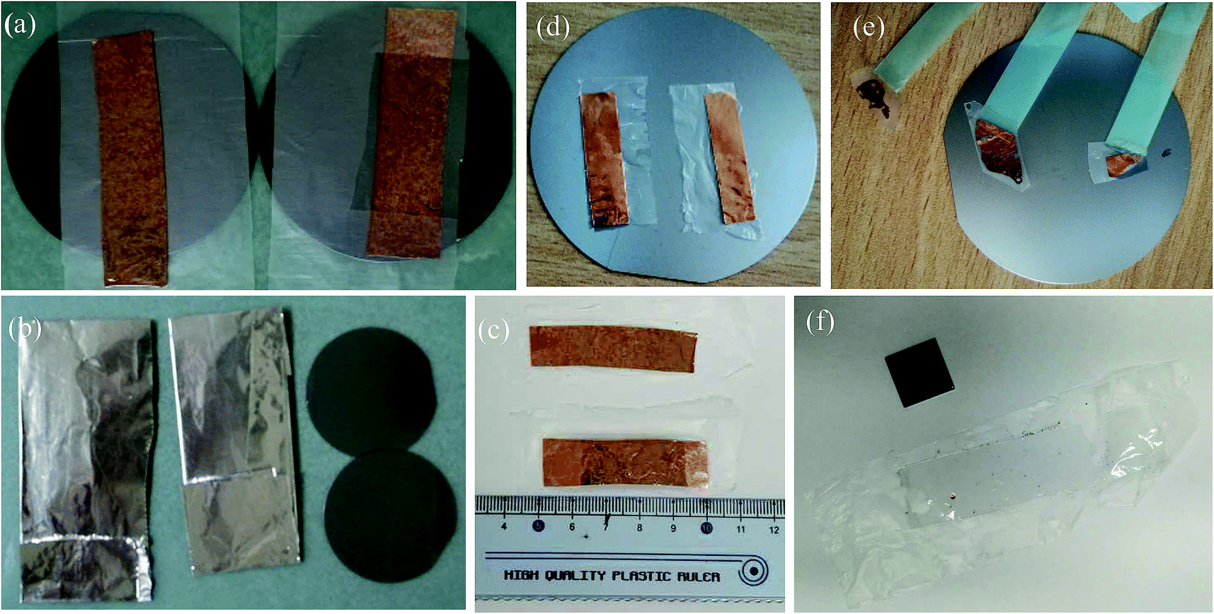 | ||
| Fig. 2 Images of samples. (a) PE/g/Cu/PE-2 and PE/g/Cu placed on 2-inch Si wafers, respectively, covered with PE film ready for aluminum foil wrapping. (b) PE/g/Cu/PE-2 and PE/g/Cu wrapped with aluminum foil and ready for attachment in a resistance furnace. (c) PE/g/Cu/PE-2 and PE/g/Cu unloaded from the furnace; (d) two PE/g/Cu/PE samples; (e) during etching the Cu foil corrodes from the outer to the inner areas. Simultaneously, parts of the Cu foil corrode due to pinholes in the PE film. (f) After Cu foil etching, PE/g/Cu becomes g/PE. Graphene is present in the smoother dark rectangular area. g/SiO2/Si is used for comparison. | ||
3.2 Graphene characterization
Fig. 3 shows optical micrographs of graphene grown on Cu foil using different growth durations. Fig. 3(a) shows well-grown isolated graphene polygons (pentagons) with sharp edges, indicating an edge-attachment-limited growth.32,33 The average size of the graphene crystal was about 20–50 μm (Fig. 2-ESI†). These crystals became larger with increasing growth time, eventually merging with each other to form a continuous sheet-like graphene film on the Cu foil, as shown in Fig. 3(b). Wrinkles were observed in the graphene film. Due to the large difference in thermal expansion coefficients between graphene and Cu foil,34,35 these wrinkles formed during cooling from the growth temperature to room temperature. After graphene was transferred to the foreign substrate, these wrinkles did not disappear, as shown in Fig. 3(c) and (d). The magnified SEM image showed no microcracks on graphene after it was transferred to the PE film (Fig. 3(e)). This indicated that the integrity of the as-grown graphene structure was unchanged after the transfer process. This might be due to the transfer involving a liquid–solid surface process,36 either for g/SiO2/Si or for g/PE. In the case of g/SiO2/Si, liquid PMMA was spin-coated onto the solid graphene surface. Due to fluid characteristics, PMMA closely contacts the graphene film at any site, such that subtle features of the graphene film remain after the transfer. In the case of g/PE, PE was heated to become molten and possessed a fluid characteristic, like that of PMMA. These two transfer processes were better than the thermal release tape process in terms of graphene integrity.37 Furthermore, PE was as good a supporting material as PMMA in the graphene transfer process.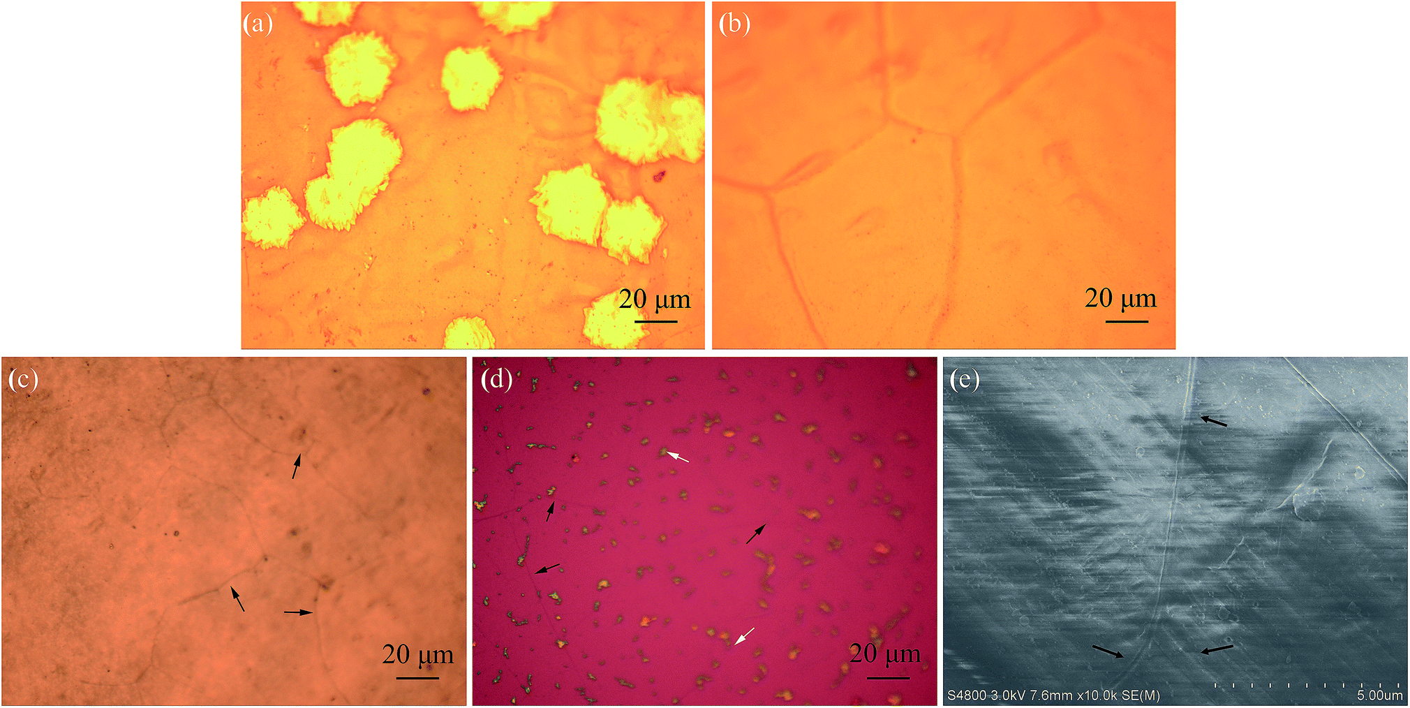 | ||
| Fig. 3 Optical microscope images of as-grown graphene and transferred graphene, and SEM image of transferred graphene on PE film. (a) Graphene crystalline grains with a polygonal shape grow on Cu foil in a short growth duration, and (b) continuous graphene film with wrinkles grows on Cu foil in a proper growth duration (g/Cu). (c) Transferred graphene on PE film (g/PE); (d) transferred graphene on SiO2/Si substrate (g/SiO2/Si); and (e) transferred graphene on PE film (g/PE). Black arrows in (c, d, and e) indicate wrinkles, and white arrows in (d) indicate contamination. | ||
Fig. 4(a)–(c) show Raman spectra in the range 1200–2800 cm−1 of as-grown graphene on Cu foil (g/Cu), transferred graphene on SiO2/Si substrate (g/SiO2/Si), and transferred graphene on PE film (g/PE), respectively. All sample spectra clearly show three peaks related to graphene at ∼1350 cm−1 (D band), ∼1590 cm−1 (G band), and 2700 cm−1 (2D band).38 The G peak and D peak arise from the E2g phonon and TO phonons at the Γ-point and around the K-point of the Brillouin zone, respectively, which are assigned to in-plane stretching of the C–C bonds and structural defects in the hexagonal ring of graphene, while the 2D peak, as the second-order D peak, is related to the phonon near the K-point.33,39 Generally, the 2D peak in the Raman spectrum is used as a fingerprint to identify graphene, and the D peak indicates graphene defects. The ratio of integrated intensity of the 2D peak to the G peak (I2D/IG), and the symmetrical characteristics of the 2D peak, are criteria for judging the graphene layer number. The I2D/IG value in Fig. 4(b) is about 2.01, which is greater than 1.8, indicating that graphene was a monolayer.40 The 2D peak was symmetrical and fitted a Lorentzian peak, which further indicated that the graphene was a monolayer. This showed that our graphene sample was a monolayer with defects. These graphene features remained unchanged, even after graphene was transferred to a foreign substrate (SiO2/Si or PE film). The Raman spectrum of g/SiO2/Si was more recognizable than those of g/Cu and g/PE, because graphene attaches to SiO2 through electrostatic adsorption and SiO2 is inactive in this Raman wavelength range, resulting in the Raman signal of g/SiO2/Si being almost identical to that of free-standing graphene. The Raman spectra of g/PE and g/Cu were harder to be recognize than that of g/SiO2/Si because chemical bonds form between graphene and the substrates (PE film or Cu foil) and these foreign substrates have Raman scattering activity. As evidence of the Raman scattering activity of the PE film, additional peaks were observed in the 1400–1500 cm−1 band in Fig. 4(c). These peaks were Raman signals of PE film, as confirmed by the Raman spectrum of pure PE film in Fig. 4(d). The effect of substrate coupling weakened the Raman signal of graphene. The 2D peak of g/PE (Fig. 4(c)) was upshifted compared with that of g/SiO2/Si (Fig. 4(b)). Previous reports have demonstrated that such Raman peak shifts are associated with deflection, strain, or doping.41–43 In our experiment, strain might be induced when graphene was transferred onto PE film, which would result in an upshift of the 2D peak.
 | ||
| Fig. 4 Raman spectra of graphene and PE film. (a) As-grown graphene on Cu foil (g/Cu); (b) transferred graphene on SiO2/Si substrate (g/SiO2/Si); (c) transferred graphene on PE film (g/PE); (d) PE film. Arrows indicate characteristic graphene peaks: black, green and red show the positions of D, G, and 2D peaks, respectively. | ||
3.3 Resistance measurements
The resistances of g/PE and Cu-2/g/PE were measured using a digital ohmmeter. Foreign Cu foil with the same amount of Cu-2 was used as the electrode for g/PE, and contacted g/PE using clips. For graphene of a similar size used as the conductor, the resistance of g/PE was found to be slightly greater than that of Cu-2/g/PE. This was probably due to the contact resistance of g/PE between foreign Cu foil and graphene being larger than that of Cu-2/g/PE. When the foreign Cu foil was replaced with aluminum foil, the resistance was almost unchanged compared with the Cu foil case. This also showed that the resistance was comparable when the clip (steel) was used directly as an electrode. This indicated that using foreign metal as an electrode was acceptable, further simplifying preparation of the g/PE sensor.To detect the response of graphene to deformation, we employed a circuit comprising a digital ammeter, a resistor, a green LED, and a set of batteries.44 A strip of Cu-2/g/PE connected by wires was used as a conductor in the circuit. The LED emitted bright light for a long-running time when the Cu-2/g/PE strip was in its normal state (Fig. 3(a)-ESI†), and the current measured by the ammeter remained almost the same. When the strip was bent, its resistance decreased (Fig. 5(a)), and the current in the circuit increased, by a factor of about 20%, producing a slightly brighter LED (Fig. 3(b)-ESI†). When the strip was recovered to its normal state from bending, its resistance was restored. Similar results were obtained when the strip was twisted (Fig. 5(b)).
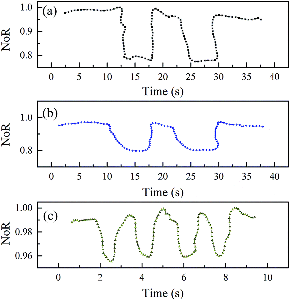 | ||
| Fig. 5 Deformation response of graphene. Normalized resistance (NoR) decreases when graphene is subjected to deformation, and is restored when deformation is unloaded. (a) Bend deformation; (b) twist deformation; (c) weak bend deformation, applied in a fixed manner via finger knuckle, loops four times. Deformation to (a) and (b) is applied in a floating manner, and loops twice. | ||
We then mounted a strip of g/PE on a finger knuckle to test the sensitivity of graphene to weak deformation. The strip was directly placed on top of the knuckle (Fig. 4(b)-ESI† insets). When the knuckle was bent, the g/PE showed weak deformation. The resistance of the g/PE was found to change, similar to a previously reported result.45 Here, a slight decrease in resistance of about 2% from the initial value was observed (Fig. 5(c)). As the change in resistance was small, the change in circuit current was also small, and the brightness of the bulb remained almost unchanged. When the knuckle was unbent, the weak deformation to the strip was unloaded, and the resistance of the g/PE was restored. This indicated that graphene could detect the response of weak deformation.
3.4 Flexible strain sensor
Next, we utilized g/PE as a flexible strain sensor to measure body signals. Body signals, such as sphygmus, can be detected by graphene-based strain sensors.4 Due to its flexibility and high sensitivity to weak deformation, g/PE would have high response to the arterial pulse. For simplicity, we prepared a sphygmus sensor by attaching a pair of clips to g/PE. Four sensor placement schemes were used in sphygmus detection. In schemes (a) and (b), the sensor was placed naturally on top of the wrist artery, while in (c) and (d), the sensor was pressed with a finger on top of the wrist artery. In schemes (a) and (d), graphene touched the skin, while in (b) and (c), the PE film touched skin. The corresponding detection results are shown in Fig. 6. The g/PE sensor detected an arterial pulse only in scheme (d), which used finger pressing with graphene directly contacting skin.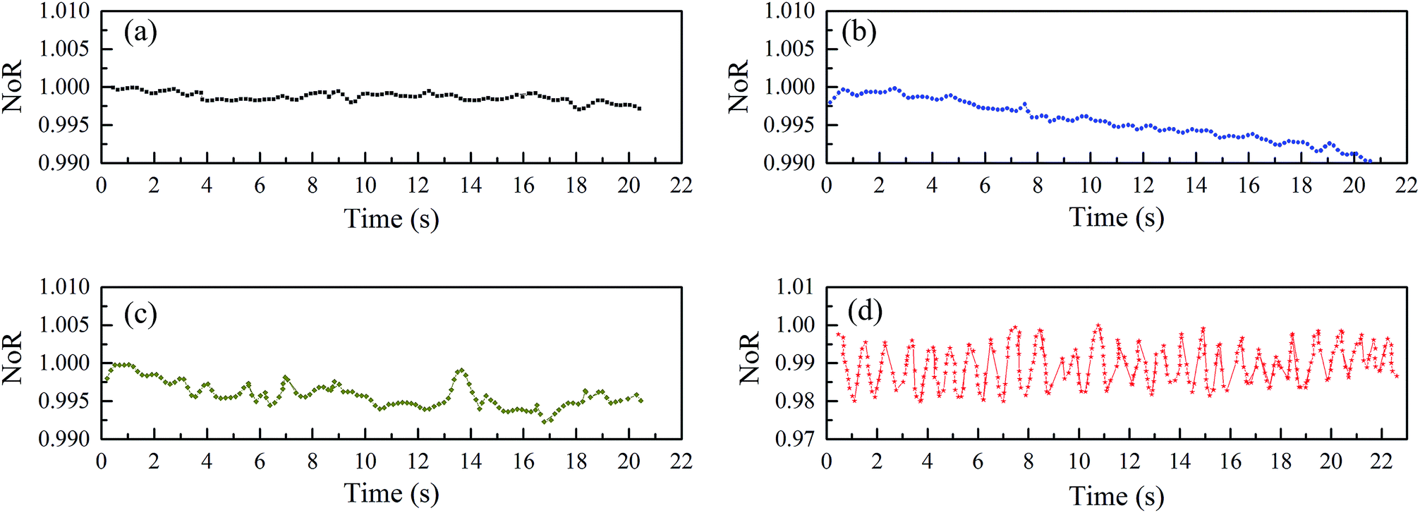 | ||
| Fig. 6 Sphygmus wave detection for the wrist artery. The graphene sphygmus sensor is made by clipping a strip of g/PE. The normalized resistance (NoR) response varies according to the placement of g/PE on the skin. (a) g/PE on top of the wrist, with the PE film touching the skin; (b) g/PE on top of the wrist, with graphene touching the skin; (c) g/PE on top of the wrist, pressed with a finger, with the PE film touching the skin; (d) g/PE on top of the wrist, pressed with a finger, with graphene touching the skin. | ||
These distinctive detection results might be due to deformation transmission from skin to graphene, which involves contact between skin and the device, the PE film, the interface between PE and graphene, and graphene itself. We proposed a model to explain this detection. When graphene is subjected to sufficient deformation, its resistance changes, which makes it operate as a sensor to respond to external signals. If the deformation is too weak, the graphene resistance changes only a little, or not at all. When the change in resistance cannot be detected by the instrument, detection fails. In scheme (a), the external signal caused by sphygmus cannot effectively deform the graphene, despite graphene contacting the skin directly to skin. The same was observed for scheme (b), in which PE film is between graphene and the skin, which screens the deformation and results in less external signal transferred to the graphene. In scheme (c), although PE film contacting the skin was enhanced by finger pressing, an insufficient signal was transferred to graphene. However, when the contact between graphene and skin was enhanced by finger pressing in scheme (d), the situation changed and the sphygmus signal was detected by the g/PE sensor.
4. Conclusions
We have demonstrated a facile process for graphene transfer to polyethylene (PE) film from copper foil and flexible strain sensor preparation based on the as-transferred graphene on PE film. PE film cut from a packing bag was used as both the supporting material for graphene transfer and the target flexible substrate. The PE film can also be used as protection mask for chemical etching of Cu foil, allowing parts of the Cu to be preserved as electrodes. The transferred graphene on PE film maintained the integrity of that grown on Cu foil. The flexible sensor made up of a strip of graphene on PE film possessed a sensitive response to deformation, such as bending and twisting. It also showed high sensitivity to weak deformation, such as the arterial pulse. This combination of graphene transfer and device preparation into a simple route makes the mass production of low-cost portable flexible sensors possible.Conflicts of interest
There are no conflicts of interest to declare.Acknowledgements
This work was supported by the National Natural Science Foundation of China (No. 31471590 and 61574140).References
- W. Chen, X. Gui, B. Liang, R. Yang, Y. Zheng, C. Zhao, X. Li, H. Zhu and Z. Tang, Structural Engineering for High Sensitivity, Ultra-Thin Pressure Sensors Based on Wrinkled Graphene and Anodic Aluminum Oxide Membrane, ACS Appl. Mater. Interfaces, 2017, 9, 24111–24117 CAS.
- S. Kundu, R. Sriramdas, K. Rafsanjani Amin, A. Bid, R. Pratap and N. Ravishankar, Crumpled sheets of reduced graphene oxide as a highly sensitive, robust and versatile strain/pressure sensor, Nanoscale, 2017, 9, 9581–9588 RSC.
- S. Liu, X. Wu, D. Zhang, C. Guo, P. Wang, W. Hu, X. Li, X. Zhou, H. Xu, C. Luo, J. Zhang and J.-H. Chu, Ultrafast dynamic pressure sensors based on graphene hybrid structure, ACS Appl. Mater. Interfaces, 2017, 9, 24148–24154 CAS.
- Y. Liu, L.-Q. Tao, D.-Y. Wang, T.-Y. Zhang, Y. Yang and T.-L. Ren, Flexible, highly sensitive pressure sensor with a wide range based on graphene-silk network structure, Appl. Phys. Lett., 2017, 110, 123508 CrossRef.
- M. Sanaeepour, A. Abedi and M. J. Sharifi, Performance Analysis of Nanoscale Single Layer Graphene Pressure Sensors, IEEE Int. Electron Devices, 2017, 64, 1292–1296 Search PubMed.
- P. Viet Phuong, N. Minh Triet, P. Jin Woo, K. Sung Soo, N. Dieu Hien Thi, M. Mu Kyeom, P. Hoang Danh, K. Doo San, K. Ki Hyun, L. Nae-Eung and Y. Geun Young, Chlorine-trapped CVD bilayer graphene for resistive pressure sensor with high detection limit and high sensitivity, 2D Mater., 2017, 4, 025049 CrossRef.
- V. M. Pereira and A. H. Castro Neto, Strain Engineering of Graphene's Electronic Structure, Phys. Rev. Lett., 2009, 103, 046801 CrossRef PubMed.
- T. Tran Quang and N.-E. Lee, Flexible and Stretchable Physical Sensor Integrated Platforms for Wearable Human-Activity Monitoring and Personal Healthcare, Adv. Mater., 2016, 28, 4338–4372 CrossRef PubMed.
- G. G. Naumis, S. Barraza-Lopez, M. Oliva-Leyva and H. Terrones, Electronic and optical properties of strained graphene and other strained 2D materials: a review, Rep. Prog. Phys., 2017, 80, 1–62 CrossRef PubMed.
- Y. Lu and J. Guo, Band Gap of Strained Graphene Nanoribbons, Nano Res., 2010, 3, 189–199 CrossRef CAS.
- M. Topsakal, V. M. K. Bagci and S. Ciraci, Current-voltage (I-V) characteristics of armchair graphene nanoribbons under uniaxial strain, Phys. Rev. B: Condens. Matter Mater. Phys., 2010, 81, 205437 CrossRef.
- X.-W. Fu, Z.-M. Liao, J.-X. Zhou, Y.-B. Zhou, H.-C. Wu, R. Zhang, G. Jing, J. Xu, X. Wu, W. Guo and D. Yu, Strain dependent resistance in chemical vapor deposition grown graphene, Appl. Phys. Lett., 2011, 99, 213107 CrossRef.
- I. Banerjee, T. Faris, Z. Stoeva, P. G. Harris, J. Chen, A. K. Sharma and A. K. Ray, Graphene films printable on flexible substrates for sensor applications, 2D Mater., 2017, 4, 015036 CrossRef.
- Z. Wang, M. Shaygan, M. Otto, D. Schall and D. Neumaier, Flexible Hall sensors based on graphene, Nanoscale, 2016, 8, 7683–7687 RSC.
- M. Xu, J. Qi, F. Li, X. Liao, S. Liu and Y. Zhang, Ultra-thin, transparent and flexible tactile sensors based on graphene films with excellent anti-interference, RSC Adv., 2017, 7, 30506–30512 RSC.
- X. Xu, J. Zhou, Y. Xin, G. Lubineau, Q. Ma and L. Jiang, Alcohol Recognition by Flexible, Transparent and Highly Sensitive Graphene-Based Thin-Film Sensors, Sci. Rep., 2017, 7, 4317 CrossRef PubMed.
- T. Wu, X. Zhang, Q. Yuan, J. Xue, G. Lu, Z. Liu, H. Wang, H. Wang, F. Ding, Q. Yu, X. Xie and M. Jiang, Fast growth of inch-sized single-crystalline graphene from a controlled single nucleus on Cu-Ni alloys, Nat. Mater., 2016, 15, 43–47 CrossRef CAS PubMed.
- X. Li, W. Cai, J. An, S. Kim, J. Nah, D. Yang, R. Piner, A. Velamakanni, I. Jung, E. Tutuc, S. K. Banerjee, L. Colombo and R. S. Ruoff, Large-Area Synthesis of High-Quality and Uniform Graphene Films on Copper Foils, Science, 2009, 324, 1312–1314 CrossRef CAS PubMed.
- M. Kim, A. Shah, C. Li, P. Mustonen, J. Susoma, F. Manoocheri, J. Riikonen and H. Lipsanen, Direct transfer of wafer-scale graphene films, 2D Mater., 2017, 4, 035004 CrossRef.
- J. Zhang, L. Lin, L. Sun, Y. Huang, A. L. Koh, W. Dang, J. Yin, M. Wang, C. Tan, T. Li, Z. Tan, Z. Liu and H. Peng, Clean Transfer of Large Graphene Single Crystals for High-Intactness Suspended Membranes and Liquid Cells, Adv. Mater., 2017, 29, 1700639 CrossRef PubMed.
- A. Capasso, M. De Francesco, E. Leoni, T. Dikonimos, F. Buonocore, L. Lancellotti, E. Bobeico, M. S. Sarto, A. Tamburrano, G. De Bellis and N. Lisi, Cyclododecane as support material for clean and facile transfer of large-area few-layer graphene, Appl. Phys. Lett., 2014, 105, 113101 CrossRef.
- S. Lee, S. K. Lee, C. G. Kang, C. Cho, Y. G. Lee, U. Jung and B. H. Lee, Graphene transfer in vacuum yielding a high quality graphene, Carbon, 2015, 93, 286–294 CrossRef CAS.
- J. W. Suk, A. Kitt, C. W. Magnuson, Y. Hao, S. Ahmed, J. An, A. K. Swan, B. B. Goldberg and R. S. Ruoff, Transfer of CVD-Grown Monolayer Graphene onto Arbitrary Substrates, ACS Nano, 2011, 5, 6916–6924 CrossRef CAS PubMed.
- A. Suhail, K. Islam, B. Li, D. Jenkins and G. Pan, Reduction of polymer residue on wet-transferred CVD graphene surface by deep UV exposure, Appl. Phys. Lett., 2017, 110, 183103 CrossRef.
- C. Holroyd, A. B. Horn, C. Casiraghi and S. P. K. Koehler, Vibrational fingerprints of residual polymer on transferred CVD-graphene, Carbon, 2017, 117, 473–475 CrossRef CAS.
- D.-Y. Wang, I. S. Huang, P.-H. Ho, S.-S. Li, Y.-C. Yeh, D.-W. Wang, W.-L. Chen, Y.-Y. Lee, Y.-M. Chang, C.-C. Chen, C.-T. Liang and C.-W. Chen, Clean-Lifting Transfer of Large-area Residual-Free Graphene Films, Adv. Mater., 2013, 25, 4521–4526 CrossRef CAS PubMed.
- G. J. M. Fechine, I. Martin-Fernandez, G. Yiapanis, R. Bentini, E. S. Kulkarni, R. V. Bof de Oliveira, X. Hu, I. Yarovsky, A. H. Castro Neto and B. Oezyilmaz, Direct dry transfer of chemical vapor deposition graphene to polymeric substrates, Carbon, 2015, 83, 224–231 CrossRef CAS.
- Z. Li, B. Du, C. Han and H. Xu, Trap Modulated Charge Carrier Transport in Polyethylene/Graphene Nanocomposites, Sci. Rep., 2017, 7, 4015 CrossRef PubMed.
- M. M. Mansor, S. K. A. Rahim and U. Hashim, A 2.45 GHz Wearable Antenna using Conductive Graphene and Polymer Substrate, 2014 1st International Symposium on Technology Management and Emerging Technologies (Istmet 2014), 2014, pp. 29–32 Search PubMed.
- M. Chen, D. Stekovic, W. Li, B. Arkook, R. C. Haddon and E. Bekyarova, Sublimation-assisted graphene transfer technique based on small polyaromatic hydrocarbons, Nanotechnology, 2017, 28, 255701 CrossRef PubMed.
- S. Kim, P. Zhao, S. Aikawa, E. Einarsson, S. Chiashi and S. Maruyama, Highly Stable and Tunable n-Type Graphene Field-Effect Transistors with Poly(vinyl alcohol) Films, ACS Appl. Mater. Interfaces, 2015, 7, 9702–9708 CAS.
- Y. F. Hao, M. S. Bharathi, L. Wang, Y. Y. Liu, H. Chen, S. Nie, X. H. Wang, H. Chou, C. Tan, B. Fallahazad, H. Ramanarayan, C. W. Magnuson, E. Tutuc, B. I. Yakobson, K. F. McCarty, Y. W. Zhang, P. Kim, J. Hone, L. Colombo and R. S. Ruoff, The Role of Surface Oxygen in the Growth of Large Single-Crystal Graphene on Copper, Science, 2013, 342, 720–723 CrossRef CAS PubMed.
- M. Borah, A. K. Pathak, D. K. Singh, P. Pal and S. R. Dhakate, Role of limited hydrogen and flow interval on the growth of single crystal to continuous graphene by low-pressure chemical vapor deposition, Nanotechnology, 2017, 28, 075602 CrossRef PubMed.
- Z. Y. Zhan, J. Sun, L. H. Liu, E. G. Wang, Y. Cao, N. Lindvall, G. Skoblin and A. Yurgens, Pore-free bubbling delamination of chemical vapor deposited graphene from copper foils, J. Mater. Chem. C, 2015, 3, 8634–8641 RSC.
- W. Z. Bao, F. Miao, Z. Chen, H. Zhang, W. Y. Jang, C. Dames and C. N. Lau, Controlled ripple texturing of suspended graphene and ultrathin graphite membranes, Nat. Nanotechnol., 2009, 4, 562–566 CrossRef CAS PubMed.
- Z. F. Shan, Q. Y. Li, Z. J. Zhao, Z. Z. Wang, Y. Q. Wu and W. W. Cai, One-step transfer and doping of large area graphene by ultraviolet curing adhesive, Carbon, 2015, 84, 9–13 CrossRef CAS.
- A. V. Zaretski and D. J. Lipomi, Processes for non-destructive transfer of graphene: widening the bottleneck for industrial scale production, Nanoscale, 2015, 7, 9963–9969 RSC.
- S. Rahimi, L. Tao, S. F. Chowdhury, S. Park, A. Jouvray, S. Buttress, N. Rupesinghe, K. Teo and D. Akinwande, Toward 300 mm Wafer-Scalable High-Performance Polycrystalline Chemical Vapor Deposited Graphene Transistors, ACS Nano, 2014, 8, 10471–10479 CrossRef CAS PubMed.
- X. F. Liu, Y. Chen, C. Z. Sun, M. Guan, Y. Zhang, F. Zhang, G. S. Sun and Y. P. Zeng, Surface Evolution of Nano-Textured 4H-SiC Homoepitaxial Layers after High Temperature Treatments: Morphology Characterization and Graphene Growth, Nanomaterials, 2015, 5, 1532–1543 CrossRef CAS PubMed.
- S. X. Cai, Z. H. Liu, N. Zhong, S. B. Liu and X. F. Liu, Effect of Growth Pressure on Epitaxial Graphene Grown on 4H-SiC Substrates by Using Ethene Chemical Vapor Deposition, Materials, 2015, 8, 5586–5596 CrossRef PubMed.
- D. Metten, G. Froehlicher and S. Berciaud, Monitoring electrostatically-induced deflection, strain and doping in suspended graphene using Raman spectroscopy, 2D Mater., 2017, 4, 014004 CrossRef.
- E. del Corro, L. Kavan, M. Kalbac and O. Frank, Strain Assessment in Graphene Through the Raman 2D'Mode, J. Phys. Chem. C, 2015, 119, 25651–25656 CAS.
- C. Neumann, S. Reichardt, P. Venezuela, M. Droegeler, L. Banszerus, M. Schmitz, K. Watanabe, T. Taniguchi, F. Mauri, B. Beschoten, S. V. Rotkin and C. Stampfer, Raman spectroscopy as probe of nanometre-scale strain variations in graphene, Nat. Commun., 2015, 6, 8429 CrossRef CAS PubMed.
- B. Deng, P. C. Hsu, G. C. Chen, B. N. Chandrashekar, L. Liao, Z. Ayitimuda, J. X. Wu, Y. F. Guo, L. Lin, Y. Zhou, M. Aisijiang, Q. Xie, Y. Cui, Z. F. Liu and H. L. Peng, Roll-to-Roll Encapsulation of Metal Nanowires between Graphene and Plastic Substrate for High-Performance Flexible Transparent Electrodes, Nano Lett., 2015, 15, 4206–4213 CrossRef CAS PubMed.
- S.-H. Bae, Y. Lee, B. K. Sharma, H.-J. Lee, J.-H. Kim and J.-H. Ahn, Graphene-based transparent strain sensor, Carbon, 2013, 51, 236–242 CrossRef CAS.
Footnote |
| † Electronic supplementary information (ESI) available. See DOI: 10.1039/c7ra09492b |
| This journal is © The Royal Society of Chemistry 2017 |