DOI:
10.1039/C7RA09473F
(Paper)
RSC Adv., 2017,
7, 50648-50656
Enhancement of thermoelectrical performance in Au-ion implanted V2O5 thin films
Received
26th August 2017
, Accepted 21st October 2017
First published on 1st November 2017
Abstract
The present study reports an enhancement of thermoelectric performance in Au ion implanted V2O5 thin films. Structural studies reveal the formation of nanocrystalline Au clusters in the Au ion implanted V2O5 thin films and some reduction of V2O5 phase into VO2 phase due to the defects created by Au ion implantation. The electrical resistivity (ρ) of thin films is decreased by about a factor of 4 upon Au ion implantation, but the magnitude of the Seebeck coefficient |S| decreases from 477.90 to 343.11 μV K−1, and results in a significant increase of the power factor (PF). Engineering of the electronic density of states (DOS) and the energy filtering mechanism (EFM) are two different approaches that can improve the PF. However, a successful combination of these two methods is elusive. The present study demonstrates that the PF of Au implanted V2O5 thin films can be significantly promoted by both these effects. Simultaneous resonant distortions in DOS and EFM result in the enhancement in PF from 1.18 × 10⁻⁸ to 3.51 × 10⁻⁵. This study may pave a way to prepare high-performance oxide based thermoelectric devices.
1. Introduction
Thermoelectric (TE) materials have attracted a great deal attention in recent years due to their ability to convert heat directly into electricity.1,2 The conversion efficiency of a thermoelectric material is described by the figure of merit, ZT, defined as: ZT = (S2σ/κ) T = S2σT/(κe + κl), where σ is the electrical conductivity, S is the Seebeck coefficient, T is the absolute temperature, and κ is the total thermal conductivity including the contributions from electrons (κe) and lattice (κl).3–6 Generally, high ZT needs a large power factor (PF = S2σ), a low κ, or both. Both Bi2Te3 and PbTe are conventional thermoelectric materials that have high ZT, and have been commonly utilized in bulk forms.7–9 In spite of their better thermoelectric properties in the bulk form, there are numerous difficulties in utilizing them in thin film forms for high temperature applications due to structural degradation and oxidation. For example, PbTe thin films change their thermoelectric properties through surface oxidation,10 and (Bi, Sb)2(Te, Se)3 hot junctions suffer from increased resistance due to oxidation above 260 °C.11 Oxides are naturally advantageous in their use at high temperatures and thus, a number of oxide systems have been investigated recently.12,13 Present study focuses on the properties of vanadium pentaoxide (V2O5) thin films as a thermoelectric device material.
The V2O5 has highest oxidation state in the V–O system and consequently the most stable one among these vanadium oxides with wide optical bandgap ∼2.24 eV.14,15 It has a lamellar, or sheet like structure.16 It is a distorted orthorhombic structure, and this deformation creates its sheet formation. These properties make V2O5 thin films a suitable candidate for scientific, industrial and technological applications, including catalytic material in gas sensors,17,18 as a dielectric constituent material in super capacitors,19 as a high capacity storage medium and as a cathode in Li-ion batteries,20 or as a thermo-resistive material in thermal infrared detectors.21 Metal to insulator transition (MIT) at ∼280 °C in V2O5 by lattice distortion and a structural inhomogeneity due to the vanadyl-oxygen vacancies reported recently,22–24 makes V2O5 a promising material for thermoelectric devices. In the insulating phase V2O5 possesses practically good value of S.25,26 However, due to its relatively large bandgap, electron hopping is dominant transport processes where it accompanies lattice distortion, bearing small polaron hopping conduction. The V ions in V2O5 exist in the oxidation states of V4+ or V5+, and the V4+ population is essentially equivalent to the small polaron population. The low concentration of the small polarons in V2O5 comes from the unintentional dopants and/or oxygen vacancies. Further, small polaron hopping materials tend to have low charge carrier mobility (μ).27 Both the small number of polarons and low μ reveal the low σ of V2O5 that results small PF and ZT, thus making the material incompatible for any practical thermoelectric applications. Since V2O5 is a non-toxic abundant material28 found in several mineral resources29 there is a significant motivation to improve its σ, to acquire large power factor (PF) and better thermoelectric figures of merit (ZT), thus removing the impediment towards its extensive use for thermoelectric applications. Recently, the Density Functional Theory (DFT) simulations have predicted that controlled doping of V2O5 with metal elements can improve the PF due to a larger enhancement in electrical conductivity.12 Recent studies have shown the enhancement primarily from physical–chemical interactions at the interface between the oxide and metal nanoparticles.9,30,31 Metal like Ag ion is noble metal that is known to form nanoclusters when implanted in materials.9,30 Similarly, Au nanoparticles is expected to provide evidence to suggest that the enhanced active site is the interface between the two metals. These also possess significant amount of free electrons that are likely to modify the electrical and thermal properties of these oxides leading to significant enhancement in S. These results have also been confirmed experimentally, for example, Na alloying has been shown to lead to a significant enhancement of the PF from 10−8 W K−2 m−1 to 10−5 W K−2 m−1.31 In this communication, we report the effect of Au ion implantation on thermoelectrical performance of V2O5 thin films.
2. Experimental details
Thin films of V2O5 were fabricated on quartz substrates by inorganic sol gel with spin coater. 0.3 grams of V2O5 (Sigma Aldrich, purity >99.9%) was dissolved in 30 ml, 30% hydrogen peroxide H2O2 (Sigma Aldrich) solution at room temperature with vigorous stirring using a magnetic stirrer till clear yellow solution is formed. This yellow solution was then heated at 60 °C on hot plate magnetic stirrer with continuous stirring to evolve excess oxygen by decomposition of H2O2 until the solution turned into red brown viscous gel. The overall mechanism is given in reactions as follows:32
| V2O5 + 2H2O2 → 2HVO4 + H2O |
| 2HVO4 + (n − 1)H2O → V2O5·nH2O + O2 + H2O |
After aging for 24 hours, the V2O5 gel was accessible for coating and spin coater (SpinNXG-P1: made by Apex Instruments, India) was used to fabricate thin films on the quartz substrates. Before deposition, substrates were cleaned in dilute sulfuric acid for 45 minutes and then thoroughly rinsed in ethanol, acetone and de-ionized water subsequently. Ten successive coatings of V2O5 gel were performed on each substrate with each coating at the rate of 3000 rpm for 30 seconds and after each coating the films were dried at 80 °C for 20 minutes. Finally these V2O5 gel films were crystallized by annealing at 450 °C for 4 hours in the ambient atmosphere in programmable tubular furnace (Nabertherm GmbH Tube furnace: RHTC80) with heating and cooling rate of 3 °C per minute. These crystallized films were then vertically exposed to Au− ion beam with energy 100 keV, at various ion fluencies: 5 × 10¹⁵ ions per cm2, 1 × 10¹⁶ ions per cm2 and 5 × 10¹⁶ ions per cm2 using Negative Ion Facility at Inter-University Accelerator Centre (IUAC), New Delhi. The implantation was carried out at room temperature and pressure was maintained at 10−6 torr. For uniform implantation, the focused beam was allowed to scan over an area of 1 × 1 cm2. After implantation the pristine and ion implanted films were again annealed in the ambient atmosphere for 1 hour at 400 °C. For convenience hereafter, the pristine as-deposited V2O5 thin films will be referred as P and the films implanted by Au ions at the ion fluences 5 × 10¹⁵, 1 × 10¹⁶ and 5 × 10¹⁶ as I5E15, I1E16 and I5E16 respectively. X-ray diffraction (XRD) measurements at room temperature in the 2θ range of 15–50° was performed to identify the crystalline phases and structure of the films using a Bruker D8 advance diffractometer with Cu Kα (0.15406 nm) X-ray source at a scan speed of 0.5° per min. Raman spectroscopy was performed using an Invia microRaman setup from Renishaw. The Ar ion laser with wavelength 488 nm, power 5 mW and exposure time of 40 seconds, was used in the Raman measurement. The Hall effect measurement was carried out by Ecopia HMS-3000 Hall Measurement System at room temperature to evaluate charge carrier density and mobility. The electrical resistivity (ρ) and thermoelectric power (S) of the films were measured in the temperature range from 300 to 400 K using DC standard four probe technique and bridge method,33 respectively. The thickness was ∼300 nm with the roughness typically in the order of ∼30 nm. Since all the samples were grown under identical conditions by spin coating and ion implantation was performed after complete annealing of samples, the thickness, roughness etc. of all the samples are similar. The set up mentioned in ref. 33 was used for thermopower measurement and hence the error in the measurement is within 3%. The Hall effect measurements were done 4 times and average value is used for discussion.
3. Results and discussions
3.1. Structural studies
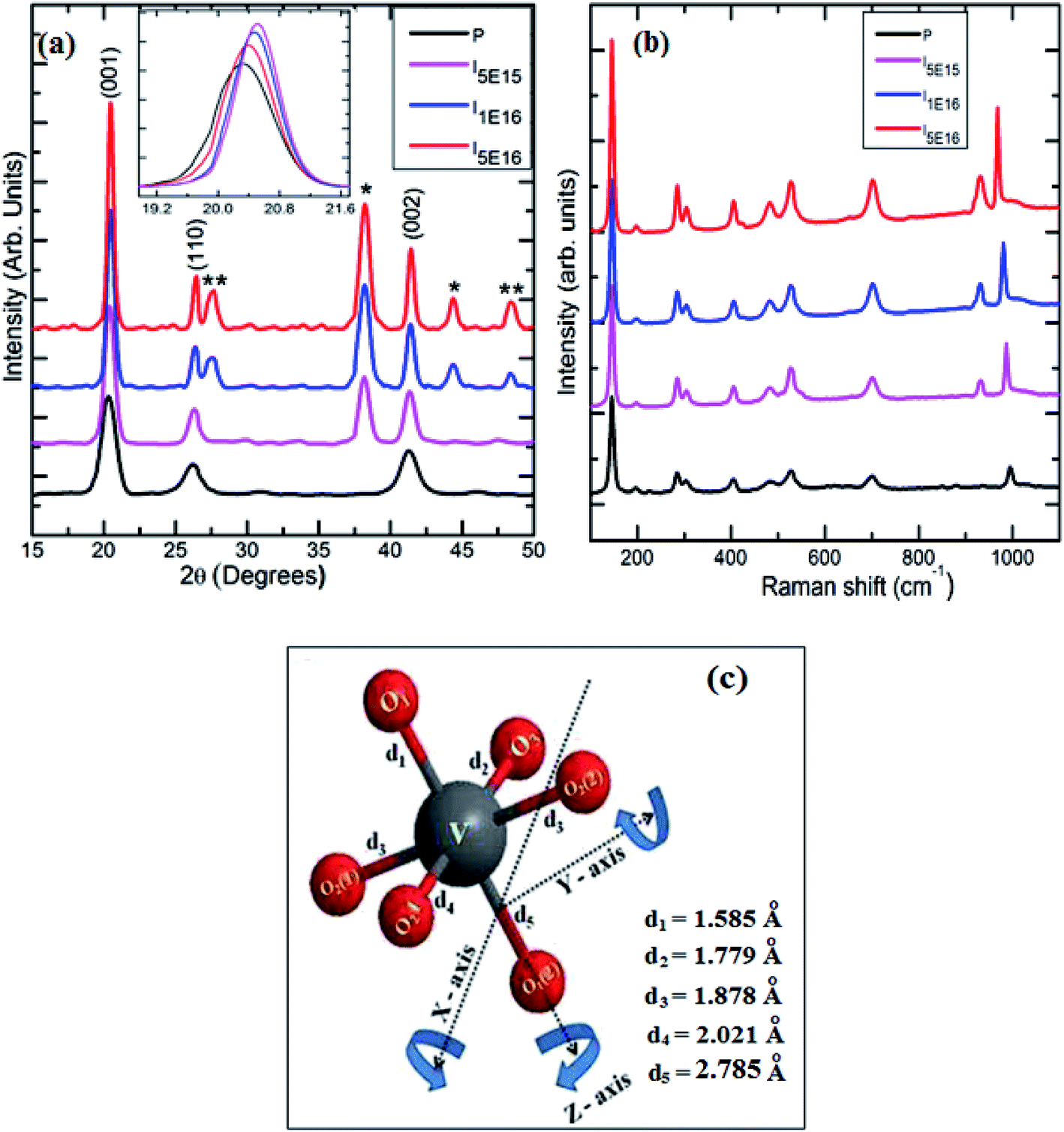
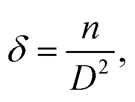
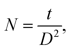
The typical XRD patterns and Raman spectra for P, I5E15, I1E16 and I5E16 are shown in Fig. 1(a) and (b). The peaks at 20.27°, 26.22° and 41.25°, correspond to reflections from (001), (110) and (002) planes (see Fig. 1(a)) of the polycrystalline orthorhombic V2O5 phase (Pmmn space group symmetry, D2h point group) with lattice constants a = 11.51 Å, b = 3.56 Å and c = 4.37 Å [JCPDS file no. #41-1426]. Absence of any other peak corresponds to any impurity or any other oxide of V in P indicates phase purity of pristine specimen. Large intensity of (001) peak at 2θ = 20.27° suggests a preferential growth along the (001) planes. The V2O5 crystal structure projected along (001) lattice plane is depicted by the geometrical diagram with its characteristics interatomic distance is shown in Fig. 1(c).34 The V atom and the three inequivalent oxygen positions O3 (bridge), O1 (vanadyl) and O2 (chain) are shown along with the bonds between the V and the nearest neighbouring oxygen atoms. In the y direction, the linear chain oxygen atoms are linked together with V atoms and in the x direction, the V atoms are connected by the bridge oxygen atoms. The bond length of V and O atoms are 1.779 Å (V–O3), 1.878 Å (V–O2(2)) and 2.021 Å (V–O2(1)). The vanadyl oxygens are positioned above and below the V atoms creating variable V–O distances the shortest (1.585 Å) and longest (2.785 Å) in this structure along the z direction. This structure can be described as a ladder structure with the legs running along y direction with rungs along x direction.35 Each V atom and its five nearest O neighbours create VO5 pyramids which split their corners within the ladder and their edges between neighbouring ladders. The resulting layers are stacked along the c direction and the V is in fact shifted out of the base plane of the pyramid toward the vanadyl oxygen.35 The peaks at 38.15° in I5E15, I1E16 & I5E16 and at 44.35° in I1E16, I5E16 correspond to (111) and (200) reflections respectively from face centered cubic Au phase (JCPDS card no 021095, space group Fm3m). The broadness of Au peaks in the diffraction patterns indicates clearly the formation of nanocrystalline Au clusters in the Au ion implanted V2O5 thin films and increase in intensity of these peaks indicates that density of size of Au nanoparticles increases with increase in ion fluences. This indicates most of Au in the film is separated particles.
 |
| | Fig. 1 (a) XRD spectra of pristine and ion implanted specimens. The ‘*’ indexed peaks corresponds to face centered cubic Au phase and the ‘**’ indexed peaks corresponds to VO2 monoclinic phase. (b) Raman spectra of pristine and ion implanted specimens. (c) Geometrical 3D view of V2O5 structure with the characteristic interatomic distances.34 | |
The peak appearing at 27.43°, and 48.44° in I1E16 and I5E16 correspond to reflections from (011), and (300) planes of the monoclinic VO2 phase [JCPDS card no 82-0661, space group P21/C]. Increase in the intensity of these peaks with ion fluence signifies reduction of V2O5 into VO2 and thus increase in V4+ population upon ion implantation. Inset of the Fig. 1(a) presents magnified view of V2O5 (001) peak. An increase in peak intensity, decrease in full width at half maxima (FWHM), and slight shift towards higher 2θ are noticed as shown in the inset with ion implantation demonstrating the decrease of adjacent interplanar (d) spacing and the improvement in crystalline nature of V2O5 films with ion implantation. The average crystallite size (D) of the V2O5 is estimated from V2O5 (001) reflection plane by using the Scherrer's formula.36 The microstrain ‘ε’ is calculated from the relation:36
| |
 | (1) |
The dislocation density (δ) defined as the length of dislocation lines per unit volume of the crystal and to be determined from the crystallite size (D) by the relation:36
| |
 | (2) |
where
n is an integer and
n = 1 gives minimum dislocation density. The number of crystallites/area (
N) is calculated using the formula:
36| |
 | (3) |
where
t is film thickness. The texture coefficient corresponding to [
hkl] miller plane (
Tc(
hkl)) is calculated from the formula:
36| |
 | (4) |
where
I(
hkl) is the measured relative intensity of a plane (
hkl),
I0(
hkl) is the standard relative intensity of the plane (
hkl) taken from the JCPDS card,
n is the number of reflections. Stacking fault probability was calculated from the formula,
| |
 | (5) |
Table 1 shows the variation of microstructural parameters such as crystallite size, interplanar spacing, microstrain, dislocation density, number of crystallites, texture coefficient, and stacking fault probability for pristine and Au ion implanted V2O5 thin films estimated from the XRD analysis of the samples at the main intensity peak of (001) of V2O5. It is evident from Table 1 that D increase, whereas d, and ε decrease with ion implantation. The increase in grain size in implanted films may be due to the diffusion of Au-ions into V2O5, which provide nucleation site for grain growth and hence increases the crystallinity.20 The microstrain values of P, I5E15, I1E16 and I5E16 are found to be 0.25, 0.22, 0.19, and 0.18 nm respectively. The evaluated microstrain values are inversely proportional to the crystallite size of the films. This may be due to an enhancement of internal microstrain with decrease in crystallite size of the films.37 Dislocation density, number of crystallites and texture coefficient decrease with increase in ion fluence due to increase in grain size. Fault probability shows irregular variation first decrease, then increase and then again decrease.
Table 1 Microstructural parameters of Au ion implanted V2O5 thin films calculated from XRD analysis
| Sample |
D (nm) |
d (Å) |
ε × 10−2 (lines−2 m−4) |
δ × 1015 (lines m−2) |
N × 104 (crystallites m−2) |
Tc |
α |
| P |
10.42 |
4.37 |
0.25 |
1.31 |
54 |
1.32 |
0.023 |
| I5E15 |
12.04 |
4.35 |
0.22 |
1.03 |
37 |
1.48 |
0.015 |
| I1E16 |
15.56 |
4.32 |
0.19 |
0.84 |
28 |
1.63 |
0.029 |
| I5E16 |
16.13 |
4.33 |
0.18 |
0.78 |
25 |
1.68 |
0.027 |
Raman spectroscopy is known to be a very useful technique used to characterize the structural order–disorder degree at short range and crystallinity of oxide materials. Fig. 1(b) displays the Raman spectra in the wavelength range of 100–1100 cm−1 of P, I5E15, I1E16 and I5E16. Raman spectrum of P matches with Stokes lines assigned to orthorhombic V2O5 phase.38,39 Table 2 presents the modes assigned to the peaks observed in the pristine samples. The most intense peak present at 144 cm−1 is attributed to skeleton bent vibration (B3g), while peaks located at 196, 284 and 405 cm−1 are corresponding to the bending vibrations of V![[double bond, length as m-dash]](https://www.rsc.org/images/entities/char_e001.gif) O bonds. The peaks located at 481 and 304 cm−1 are assigned to the bending vibrations of the bridging V–O–V (doubly coordinated oxygen) and V–O (triply coordinated oxygen) bonds, respectively. The peak at 527 cm−1 is attributed to the triply coordinated oxygen atom (V3–O) stretching mode, aroused from the edge-shared oxygen atoms common to three VO5 pyramids. The peak positioned at 701 cm−1 is attributed to the doubly coordinated oxygen (V2–O) asymmetric stretching mode which originates from corner shared oxygen common to two VO5 pyramids. The high frequency peaks at 995 cm−1 corresponds to the stretching mode of terminal oxygen (VO) which arises from an unshared oxygen. No other peaks representing secondary phases of V and O were observed in Raman spectra of P that ascertains phase purity of pristine samples. The high frequency Raman peak at 995 cm−1 that corresponds to the stretching mode of terminal oxygen (VO) gives the structural quality of the films and can be ascribed to the stretching mode related to the Ag symmetry vibrations of the of the shortest V and O bond, which is VO. Unlike the other O atoms this atom is strongly bonded to only one V atom and for this reason is called terminal O.40 The frequency shift of this mode measures the deviations from stoichiometry. The frequency shift to lower values of this mode is due to softening of the V5+O bond in oxygen deficient V2O5 films, resulting from vacancies created by removing OV, with some of the V5+ reduced to V4+ in order to balance the charge. Negligible frequency shift of this mode manifests good stoichiometry of pristine samples. The shift in the peak position of 986, 980, and 968 cm−1 for I5E15, I1E16 and I5E16 respectively indicates that some reduction of V5+ to V4+ upon Au ion implantation in V2O5 thin films. This is also evident as a peak corresponding to V4+O near 932 cm−1 is observed in ion beam implanted V2O5 thin films.41 Enhancement in peak intensities in ion implanted thin films indicates that the crystallinity increases with ion implantation. Absence of peak at 850 cm−1 indicates that the films are not hydrated (V2O5·H2O) which is normally observed in V2O5 as contaminant.42 The presence of peak at 141 cm−1 and 194 cm−1 in P, I5E15, I1E16 and I5E16 confirms that layer-like structure is retained after ion implantation.39 During ion implantation oxygen vacancies are created. Such vacancies result in reducing the oxidation state of V and hence some of the V2O5 reduces into VO2. Similar results of reduction of oxides of Fe, Co, Ti and Nb by low-energy ion bombardment have been reported by Choudhury et al.43
O bonds. The peaks located at 481 and 304 cm−1 are assigned to the bending vibrations of the bridging V–O–V (doubly coordinated oxygen) and V–O (triply coordinated oxygen) bonds, respectively. The peak at 527 cm−1 is attributed to the triply coordinated oxygen atom (V3–O) stretching mode, aroused from the edge-shared oxygen atoms common to three VO5 pyramids. The peak positioned at 701 cm−1 is attributed to the doubly coordinated oxygen (V2–O) asymmetric stretching mode which originates from corner shared oxygen common to two VO5 pyramids. The high frequency peaks at 995 cm−1 corresponds to the stretching mode of terminal oxygen (VO) which arises from an unshared oxygen. No other peaks representing secondary phases of V and O were observed in Raman spectra of P that ascertains phase purity of pristine samples. The high frequency Raman peak at 995 cm−1 that corresponds to the stretching mode of terminal oxygen (VO) gives the structural quality of the films and can be ascribed to the stretching mode related to the Ag symmetry vibrations of the of the shortest V and O bond, which is VO. Unlike the other O atoms this atom is strongly bonded to only one V atom and for this reason is called terminal O.40 The frequency shift of this mode measures the deviations from stoichiometry. The frequency shift to lower values of this mode is due to softening of the V5+O bond in oxygen deficient V2O5 films, resulting from vacancies created by removing OV, with some of the V5+ reduced to V4+ in order to balance the charge. Negligible frequency shift of this mode manifests good stoichiometry of pristine samples. The shift in the peak position of 986, 980, and 968 cm−1 for I5E15, I1E16 and I5E16 respectively indicates that some reduction of V5+ to V4+ upon Au ion implantation in V2O5 thin films. This is also evident as a peak corresponding to V4+O near 932 cm−1 is observed in ion beam implanted V2O5 thin films.41 Enhancement in peak intensities in ion implanted thin films indicates that the crystallinity increases with ion implantation. Absence of peak at 850 cm−1 indicates that the films are not hydrated (V2O5·H2O) which is normally observed in V2O5 as contaminant.42 The presence of peak at 141 cm−1 and 194 cm−1 in P, I5E15, I1E16 and I5E16 confirms that layer-like structure is retained after ion implantation.39 During ion implantation oxygen vacancies are created. Such vacancies result in reducing the oxidation state of V and hence some of the V2O5 reduces into VO2. Similar results of reduction of oxides of Fe, Co, Ti and Nb by low-energy ion bombardment have been reported by Choudhury et al.43
Table 2 Raman peaks observed in pristine samples along with assignment of bands
| Peak |
Band assigned |
| 144 |
Skeleton bent vibration (B3g species) |
| 196 |
VO bending mode (Ag mode) |
| 284 |
VO bending mode (B2g mode) |
| 304 |
Rx liberation mode (Ag species) |
| 405 |
VO bending mode (Ag mode) |
| 481 |
V–O–V bending vibration |
| 527 |
Triply coordinated oxygen (V3–O) (Ag species) |
| 701 |
Doubly coordinated oxygen (V2–O) stretching mode (B2g and B3g species) |
| 995 |
Terminal oxygen (VO) stretching mode |
3.2. Electrical and thermo electrical studies
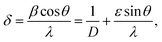
The temperature dependence of electrical resistivity (ρ), for P, I5E15, I1E16, and I5E16, in the temperature range 300–400 K is shown in Fig. 2(a). Decrease in ρ with temperature indicates that the samples exhibit semiconducting behavior in this temperature range. Further, in the entire temperature range the resistivity decreases in the order: P > I5E15 > I1E16 > I5E16. The resistivity of P, I5E15, I1E16, and I5E16 at room temperature are 21.101, 0.080, 0.012, and 0.003 (Ω m) respectively (see Table 3). Fig. 2(b) shows the carrier concentration (n) and mobility (μ) of the films measured at room temperature for specimens. The value of n increases rapidly with Au ion implantation and μ decreases due to the impurity scattering by implanted ions. The measured carrier concentrations are ∼2.20 × 1016 cm−3, ∼2.08 × 1017 cm−3, ∼8.91 × 1017 cm−3, and ∼4.60 × 1018 cm−3 and carrier mobility are ∼5.82, ∼3.57, ∼2.11, and ∼1.36 for P, I5E15, I1E16, and I5E16, respectively (Table 3). The decrease in ρ is attributed to the increased carrier concentration by Au ion implantation, despite of the slight decrease in Hall mobility. Iwanaga et al. investigated the effect of Na alloying in V2O5 and observed a significant enhancement of thermopower.31 It was also demonstrated by them that increasing Na concentration increases the electrical conductivity by a factor of up to ∼104, whereas the S decreased only by a half and the power factor improved upto 350 times. Similarly Lourerio et al. observed that by Cr doping the thermoelectric properties are enhanced significantly.13 Presence of nanograins in the films are responsible for an improvement of electrical and thermal properties. Bala et al. also showed that addition of Au either by chemical addition or by ion implantation results in better properties in PbTe.30,31 Present investigation is consistent with above results.
 |
| | Fig. 2 (a) Electrical resistivity verses temperature of specimens. (b) Carrier density and carrier mobility of samples. (c) Seebeck coefficient as a function of temperature of samples. | |
Table 3 Room temperature electrical resistivity, carrier concentration, carrier mobility, Seebeck coefficient, power factor, band gap and effective mass of for the P, I5E15, I1E16, and I5E16 samples
| Specimen |
ρ (Ω m) |
n (cm−3) |
μ (cm2 V−1 s−1) |
S (μV K−1) |
PF (W K−2 m−1) |
Ea (eV) |
m* |
| P |
21.101 |
2.20 × 10¹⁶ |
5.82 |
−477.93 |
1.08 × 10⁻⁸ |
2.17 |
1.52me |
| I5E15 |
0.080 |
2.08 × 10¹⁷ |
3.57 |
−420.15 |
2.21 × 10⁻⁶ |
2.06 |
2.18me |
| I1E16 |
0.012 |
8.91 × 10¹⁷ |
2.11 |
−374.17 |
1.40 × 10⁻⁵ |
1.99 |
2.68me |
| I5E16 |
0.003 |
4.60 × 10¹⁸ |
1.36 |
−343.11 |
3.90 × 10⁻⁵ |
1.95 |
3.06me |
To further investigate the influence of Au ion implantation, the activation energy (Ea) was anticipated from the slope of linear fit of ln(ρ) vs. 1000/T curve (Fig. 3(a)) according to the Arrhenius formula:44
| |
ρ = ρ0![[thin space (1/6-em)]](https://www.rsc.org/images/entities/char_2009.gif) exp(Ea/2KbT) exp(Ea/2KbT)
| (6) |
where
ρ is the electrical resistivity and
ρ0 is a constant. The calculated values of
Ea are 2.17, 2.06, 1.99 and 1.95 eV for the
P,
I5E15,
I1E16, and
I5E16 samples, respectively (
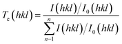
Fig. 3(b)). It can thus be concluded that the activation energy decreases with Au content. This is consistent with the increase in carrier concentration and decrease in electrical resistivity.
 |
| | Fig. 3 (a) ln(ρ) vs. 1000/T plot. (b) The calculated activation energy and power factor of specimens. (c) Variation of Seebeck coefficient with carrier concentration. Red solid line represents the carrier concentration dependence of S without any secondary effect. Blue Dashed represents the carrier concentration dependence of S considering only electronic DOS. | |
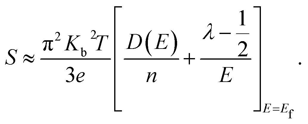
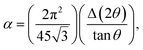
The variations of thermoelectric power (S) of the specimens are shown in Fig. 2(c). Negative value S reflects dominant n-type conduction mechanism in the specimens. The temperature dependences of S shows that |S| increase with temperature for all the specimens. Further, |S|, decrease with ion implantation. The measured values of S for P, I5E15, I1E16 and I5E16 films at room temperature are −477.93, −420.15, −374.17, and −343.11 μV K−1 respectively (Table 3). Large increase in electrical conductivity in comparison to small decrease in |S| results an overall increase in power factor (PF = S2σ). The PF of P, I5E15, I1E16, and I5E16 at room temperature are ∼1.18 × 10⁻⁸, ∼2.21 × 10⁻⁶, ∼1.40 × 10⁻⁵ and 3.51 × 10⁻⁵ W K−2 m−1 respectively. Generally, there is a tradeoff between the S and the σ since S and σ vary in a reciprocal way, and both the values are also dependent on each other with carrier density (n). Increasing n usually results in decrease in the S in accordance with increase in σ and thus prevents any enhancement in PF and ZT. However, in present work, there is only slight decrease in S with Au ion implantation of V2O5 thin films in spite of appreciable increase in σ by factor 104, leads to increase in PF. Since Ea for all the samples is larger than 3KT (75 meV) therefore all the samples belong to degenerated semiconductors. According to the Mott, the thermopower S of a degenerate semiconductor, can be expressed as:45
| |
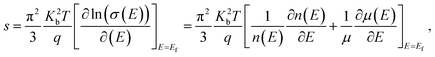 | (7) |
where
σ is the electrical conductivity,
q is the carrier charge,
n(
E) and
μ(
E) are energy dependent charge carrier density and carrier mobility,
λ is the scattering parameter,
Kb is the Boltzmann constant,
m* is the effective mass and
Ef the Fermi energy. With the approximation of a free-electron gas and assuming an exponential dependence of the scattering parameter
λ on the relaxation time
τ,
i.e. τ =
τ0Eλ−1/2 (here
τ0 is an energy-independent constant),
eqn (7) can be written as:
| |
 | (8) |
Here
D(
E) is the electronic density of states (DOS).
Eqn (8) implies that at a given carrier concentration (
n),
S can be enhanced by either increasing
D(
E),
i.e. the electronic DOS at the Fermi level, or the scattering parameter
λ that corresponds to the energy filtering mechanism (EFM).
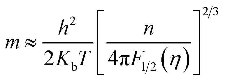
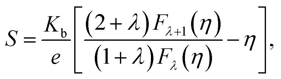
14,46 The effective mass
m* is estimated based on the measured values of carrier concentration (
n) and thermopower (
S). Assuming a single parabolic band model with acoustic phonon scattering,
m* and
S can be approximated by:
47,48| |
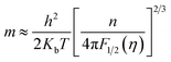 | (9) |
| |
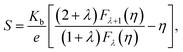 | (10) |
where
Kb is the Boltzmann constant,
h is the Planck constant,
e is elementary charge,
λ is a scattering parameter related to the energy dependence of the carrier scattering mechanism,
η (=
Ef/
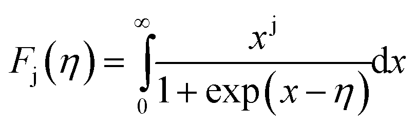
KbT) is the reduced Fermi level, and
Fj(
η) is the Fermi integral of order j and is given by:
| |
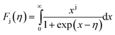 | (11) |
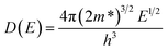
According to Heremans et al., the scattering parameter λ of doped systems without inclusions (or secondary phase) is dominated by the acoustic modes and can be zeroed.48,49 The calculated m* for P, I5E15, I1E16, and I5E16 are 1.52me, 2.18me, 2.68me and 3.06me, respectively (Table 3). The large effective mass of ion implanted samples in comparison to P specifies that there is strong resonant distortion of the electronic DOS around the Fermi level, since the DOS is directly related to effective mass m* as:50
| |
 | (12) |
Using formulae (11) and (12) and m* = 1.52me and λ = 0 for the P, one can plot the dependence of S on carrier concentration at 300 K (solid red line in Fig. 3(c)). Without resonant distortion of the electronic DOS, the thermopower S of Au implanted thin films should lie on the same line. However, it is found that S of I5E15, I1E16, and I5E16, is ∼45, ∼49 and ∼54 μV K−1 higher than the values of the solid red line, respectively (Fig. 3(c)), indicating strong electronic DOS resonant distortion effects. Further using the same formulae with and m* = 2.18me; 2.68me and 3.06me, and λ = 0, the thermopower S at 300 K for I5E15, I1E16, and I5E16 would be ∼398, ∼346, and 311 μV K−1 respectively and the method of extrapolating yields the blue dashed line in Fig. 3(C). Without energy filtering effect thermopower values of ion implanted V2O5 thin films should lie on this dotted blue line. But measured S values of I5E15, I1E16, and I5E16, are ∼23, 28, and 32 μV respectively, above the line, demonstrating that there is energy filtering effect in Au implanted thin films. It is known that ZT depends on PF and k. With implantation, the value of σ increases drastically because of large number of free electrons supplied by Au ions. Apart from this due to Au implantation, there is also nanostructuring that results due to Au clusters as evident from XRD. This contributes significantly for ke and kL which are components of k. Au and VO2 nanograins gets formed in Au ion implanted thin films as discussed in structural studies acts as nanoinclusions in the matrix of V2O5, leading to the formation of heterojunction potential barriers at the phase boundary and these potential barriers act as additional scattering centers giving rise to the EFM that contributes to the large enhancement of S.51 Above behaviours have been understood on the basis of combined effects of resonant distortion of the electronic DOS, and carrier energy filtering.
4. Conclusions
Thin films of V2O5 were fabricated on quartz substrates by simple inorganic sol-gel method and 100 keV Au− ions at various fluences were implanted in these films. The structural studies show the presence of Au and VO2 nanograins in the matrix of V2O5 upon ion implantation and these nanograins acts as nanoinculsions. Electrical transport studies exhibit that with Au ion implantation, the Seebeck coefficient decreases slightly in spite of appreciable increase in electrical conductivity by factor 104, that results in increase in power factor. This demonstrates that Au ion implantation improved the thermoelectric properties of the V2O5 thin films. The origin of such behaviour of Seebeck coefficient results from the combination of resonant distortion of the electronic DOS in the Au ion implanted V2O5 thin films and intensified by energy filtering at the heterojunction potential barriers formed due to Au and VO2 nanoinculsions. These findings will be helpful to design high-performance oxide thermoelectric devices.
Conflicts of interest
There are no conflicts to declare.
Acknowledgements
Authors thank IUAC for the Low energy ion beam facility for providing us Au ion implantation and also some of the characterization facilities.
References
- S. G. Jeffrey and E. S. Toberer, Complex thermoelectric materials, Nat. Mater., 2008, 7(2), 105–114 CrossRef PubMed.
- L.-D. Zhao, et al., Ultralow thermal conductivity and high thermoelectric figure of merit in SnSe crystals, Nature, 2014, 508(7496), 373–377 CrossRef CAS PubMed.
- Y. Pei, et al., Convergence of electronic bands for high performance bulk thermoelectrics, Nature, 2011, 473(7345), 66–69 CrossRef CAS PubMed.
- K. Biswas, et al., High-performance bulk thermoelectrics with all-scale hierarchical architectures, Nature, 2012, 489(7416), 414–418 CrossRef CAS PubMed.
- R. Venkatasubramanian, et al., Thin-film thermoelectric devices with high room-temperature figures of merit, Nature, 2001, 413(6856), 597–602 CrossRef CAS PubMed.
- K. F. Hsu, et al., Cubic AgPb(m)SbTe(2 + m): bulk thermoelectric materials with high figure of merit, Science, 2004, 303(5659), 818–821 CrossRef CAS PubMed.
- H. J. Goldsmid, The electrical conductivity and thermoelectric power of bismuth telluride, Proceedings of the Physical Society, 1958, 71(4), 633 CrossRef CAS.
- Y. Gelbstein, Z. Dashevsky and M. P. Dariel, High performance n-type PbTe-based materials for thermoelectric applications, Phys. B, 2005, 363(1), 196–205 CrossRef CAS.
- M. Bala, et al., Enhancement of thermoelectric power of PbTe:Ag nanocomposite thin films, RSC Adv., 2015, 5, 25887–25895 RSC.
- E. I. Rogacheva, S. G. Lyubchenko and M. S. Dresselhaus, Effect of oxidation on thickness dependencies of thermoelectric properties in PbTe/mica thin films, Thin Solid Films, 2005, 476.2, 391–395 CrossRef.
- C. Huang and A. Christou, Diffusion controlled degradation analysis of high temperature (Bi, Sb)2 (Te, Se) 3 semiconductor thermoelectric power modules, Mater. Sci. Eng., B, 1995, 29(1–3), 233–236 CrossRef.
- Y. Chumakov, S. Y. Xiong, J. R. Santos, I. Ferreira, K. Termentzidis, A. Pokropivny, P. Cortona and S. Volz, J. Electron. Mater., 2012, 42, 1597–1603 CrossRef.
- J. Loureiro, et al., Nanostructured p-type Cr/V2O5 thin films with boosted thermoelectric properties, J. Mater. Chem. A, 2014, 2, 6456 CAS.
- F. J. Morin, Oxides which show a metal-to-insulator transition at the Neel temperature, Phys. Rev. Lett., 1959, 3(1), 34 CrossRef CAS.
- R. L. Smith, et al., A scanning probe microscopy study of the (001) surfaces of V2O5 and V6O13, Surf. Sci., 1996, 367(1), 87–95 CrossRef CAS.
- K. Sieradzka, et al., Structural and optical properties of vanadium oxides prepared by microwave-assisted reactive magnetron sputtering, Opt. Appl., 2011, 41(2), 463–469 CAS.
- N. Izu, et al., Application of V2O5/WO3/TiO2 for resistive-type SO2 sensors, Sensors, 2011, 11(3), 2982–2991 CrossRef CAS PubMed.
- K. Hermann, et al., Ab initio density functional theory studies of hydrogen adsorption at the V2O5 (010) surface, Phys. Status Solidi A, 1999, 173(1), 195–208 CrossRef CAS.
- Y. Yang, et al., Vertically aligned mixed V2O5–TiO2 nanotube arrays for supercapacitor applications, Chem. Commun., 2011, 47(27), 7746–7748 RSC.
- A.-M. Cao, et al., Self-assembled vanadium pentoxide (V2O5) hollow microspheres from nanorods and their application in lithium-Ion batteries, Angew. Chem., Int. Ed., 2005, 44(28), 4391–4395 CrossRef CAS PubMed.
- P. W. Kruse, Uncooled thermal imaging: arrays, systems, and applications, SPIE press, 2001, vol. 51 Search PubMed.
- M. Kang, et al., Metal-insulator transition without structural phase transition in V2O5 film, Appl. Phys. Lett., 2011, 98(13), 131907 CrossRef.
- R.-P. Blum, et al., Surface metal-insulator transition on a vanadium pentoxide (001) single crystal, Phys. Rev. Lett., 2007, 99(22), 226103 CrossRef PubMed.
- A. L. Pergament, G. B. Stefanovich and A. A. Velichko, Oxide electronics and vanadium dioxide perspective: A review, Journal on Selected Topics in Nano Electronics and Computing, 2013, 1(1), 24–43 CrossRef.
- R. Santos, et al.,
Thermoelectric properties of V2O5 thin films deposited by thermal evaporation, Appl. Surf. Sci., 2013, 282, 590–594 CrossRef CAS.
- D. K. Chakrabarty, D. Guha and A. B. Biswas, Electrical properties of vanadium pentoxide doped with lithium and sodium in the α-phase range, J. Mater. Sci., 1976, 11(7), 1347–1353 CrossRef CAS.
- P. Vaqueiro and A. V. Powell, Recent developments in nanostructured materials for high-performance thermoelectrics, J. Mater. Chem., 2010, 20(43), 9577–9584 RSC.
- R. R. Moskalyk and A. M. Alfantazi, Processing of vanadium: a review, Miner. Eng., 2003, 16(9), 793–805 CrossRef CAS.
- K. Koumoto, I. Terasaki and R. Funahashi, Complex oxide materials for potential thermoelectric applications, MRS Bull., 2006, 31(03), 206–210 CrossRef CAS.
- M. Bala, et al., Enhancement of thermoelectric power of PbTe thin films by Ag ion implantation, J. Appl. Phys., 2017, 121, 215301 CrossRef.
- S. Iwanaga, et al., Thermopower and electrical conductivity of sodium-doped V2O5 thin films, J. Appl. Phys., 2007, 101(12), 123709 CrossRef.
- X. Ren, et al., Preparation and electrochemical properties of V2O5 submicron-belts synthesized by a sol–gel H2O2 route, J. Sol-Gel Sci. Technol., 2009, 51(2), 133–138 CrossRef CAS.
- T. S. Tripathi, M. Bala and K. Asokan, An experimental setup for the simultaneous measurement of thermoelectric power of two samples from 77 K to 500 K, Rev. Sci. Instrum., 2014, 85(8), 085115 CrossRef CAS PubMed.
- H.-G. Bachmann, F. Ramadan Ahmed and W. H. Barnes, The crystal structure of vanadium pentoxide, Z. Kristallog. – Cryst. Mater., 1961, 115(1–6), 110–131 CrossRef CAS.
- S. Atzkern, et al., Valence-band excitations in V2O5, Phys. Rev. B: Condens. Matter Mater. Phys., 2000, 61(19), 12792 CrossRef CAS.
- B. D. Cullity, in Elements of X-ray Diffraction, Addison-Wesley Publishing Inc, Massachusetts, U.S.A, 1956 Search PubMed.
- S. Thiagarajan, M. Thaiyan and R. Ganesan, Physical property exploration of highly oriented V2O5 thin films prepared by electron beam evaporation, New J. Chem., 2015, 39(12), 9471–9479 RSC.
- R. Baddour-Hadjean, et al., Lattice dynamics of β-V2O5: Raman spectroscopic insight into the atomistic structure of a high-pressure vanadium pentoxide polymorph, Inorg. Chem., 2012, 51(5), 3194–3201 CrossRef CAS PubMed.
- B. A. Bhat, G. R. Khan and K. Asokan, Role of substrate effects on the morphological, structural, electrical and thermoelectrical properties of V2O5 thin films, RSC Adv., 2015, 5(65), 52602–52611 RSC.
- P. Clauws, J. Broeckx and J. Vennik, Lattice Vibrations of V2O5. Calculation of Normal Vibrations in a Urey-Bradley Force Field, Phys. Status Solidi B, 1985, 131(2), 459–473 CrossRef CAS.
- S.-H. Lee, et al., Raman spectroscopic studies of amorphous vanadium oxide thin films, Solid State Ionics, 2003, 165(1), 111–116 CrossRef CAS.
- X. Chen, et al., Ozone-based atomic layer deposition of crystalline V2O5 films for high performance electrochemical energy storage, Chem. Mater., 2012, 24(7), 1255–1261 CrossRef CAS.
- T. Choudhury, et al., Reduction of oxides of iron, cobalt, titanium and niobium by low-energy ion bombardment, J. Phys. D: Appl. Phys., 1989, 22, 1185–1195 CrossRef CAS.
- N. F. Mott and E. A. Davis, Electronic process in non-crystalline materials, Oxford University Press, 1971 Search PubMed.
- M. Jonson and G. D. Mahan, Mott's formula for the thermopower and the Wiedemann-Franz law, Phys. Rev. B: Condens. Matter Mater. Phys., 1980, 21(10), 4223 CrossRef CAS.
- T. Zou, et al., Enhanced thermoelectric performance of β-Zn4Sb3 based nanocomposites through combined effects of density of states resonance and carrier energy filtering, Sci. Rep., 2015, 5, 17803 CrossRef CAS PubMed.
- H. Xie, et al., Beneficial Contribution of Alloy Disorder to Electron and Phonon Transport in Half-Heusler Thermoelectric Materials, Adv. Funct. Mater., 2013, 23(41), 5123–5130 CrossRef CAS.
- T. Caillat, J.-P. Fleurial and A. Borshchevsky, Preparation and thermoelectric properties of semiconducting Zn4Sb3, J. Phys. Chem. Solids, 1997, 58(7), 1119–1125 CrossRef CAS.
- J. P. Heremans, et al., Enhancement of thermoelectric efficiency in PbTe by distortion of the electronic density of states, Science, 2008, 321(5888), 554–557 CrossRef CAS PubMed.
- C. Kittel, Introduction to solid state physics, Wiley, New York, 8th edn, 2005, ch. 6, pp. 131–157 Search PubMed.
- X. H. Yang, et al., Enhanced thermopower and energy filtering effect from synergetic scattering at heterojunction potentials in the thermoelectric composites with semiconducting nanoinclusions, J. Alloys Compd., 2013, 558, 203–211 CrossRef CAS.
|
| This journal is © The Royal Society of Chemistry 2017 |
Click here to see how this site uses Cookies. View our privacy policy here. 
 Open Access Article
 This Open Access Article is licensed under a
  d,
Shafiq Maqbool Tantarye and
K. Asokan
d,
Shafiq Maqbool Tantarye and
K. Asokan