DOI:
10.1039/C7RA09441H
(Paper)
RSC Adv., 2017,
7, 50279-50286
Gas sensing performance at room temperature of nanogap interdigitated electrodes for detection of acetone at low concentration†
Received
25th August 2017
, Accepted 22nd October 2017
First published on 27th October 2017
Abstract
A facile approach for the fabrication of large-scale interdigitated nanogap electrodes (nanogap IDEs) with a controllable gap was demonstrated with conventional micro-fabrication technology to develop chemocapacitors for gas sensing applications. In this work, interdigitated nanogap electrodes (nanogap IDEs) with gaps from 50–250 nm have been designed and processed at full wafer-scale. These nanogap IDEs were then coated with poly(4-vinyl phenol) as a sensitive layer to form gas sensors for acetone detection at low concentrations. These acetone sensors showed excellent sensing performance with a dynamic range from 1000 ppm to 10 ppm of acetone at room temperature and the observed results are compared with conventional interdigitated microelectrodes according to our previous work. Sensitivity and reproducibility of devices are discussed in detail. Our approach of fabrication of nanogap IDEs together with a simple coating method to apply the sensing layer opens up possibilities to create various nanogap devices in a cost-effective manner for gas sensing applications.
Introduction
Nanogap devices have attracted numerous fundamental and application oriented studies because of their great potential in solving challenging problems at the molecular and nano scale.1 They have been widely employed not only for molecular electronics,2 and optical plasmonics,3 but also in tunneling based sensors, biosensors and chemical sensors.4,5 Their drawback preventing applications still remains a reproducible and cost-effective fabricating process yielding stable electrical contacts. Different methods have been applied to address this issue including improved fabrication processes6–9 and/or modifying the nano-electrode structures.10–12 Nanogap devices are promising to become a new generation of devices that operate fast with a high sensitivity, consume less power, and can be applied in portable devices.
Taking into account the rapid progress of gas sensing applications, detection at low concentration is one of the greatest possibilities in using nanogap devices.13–19 Up to now, there are not many studies on the detection of volatile organic compounds (VOCs) with nanogap devices. To investigate gas-sensing properties of nanogap devices towards VOCs for air quality control is an appealing challenge. For example, acetone, one of the most common VOCs, is widely used in the industry and laboratory for synthesis, solvent, cleaning agent, etc. It is a nontoxic agent at a low concentration, but acetone can cause harm and danger to human health when it exceeds specific threshold values, and can also affect environmental safety. A high concentration of acetone can cause to the human body several syndromes: fatigue, headache and nausea when being inhaled,20 irritated eyes and skin or throat damage when being exposed when its concentration are above 10![[thin space (1/6-em)]](https://www.rsc.org/images/entities/char_2009.gif) 000 ppm.21,22 Not only being widely used for in-house air quality control but acetone sensors have been further exploited for medical diagnosis as well. A number of recent investigations prove that acetone, as one of the biomarkers in human breath, represents for diabetes diagnosis because a relatively high concentration can be an indication of diabetes.23–25 Therefore, it is essential and significant to effectively detect acetone gas in different ranges of concentration.
000 ppm.21,22 Not only being widely used for in-house air quality control but acetone sensors have been further exploited for medical diagnosis as well. A number of recent investigations prove that acetone, as one of the biomarkers in human breath, represents for diabetes diagnosis because a relatively high concentration can be an indication of diabetes.23–25 Therefore, it is essential and significant to effectively detect acetone gas in different ranges of concentration.
Inspired by these promising goals in the field of sensing devices, we focused on the exploration of gas sensing properties of nanogap IDEs. There has been significant progress in realizing structures for nanogap devices, however, the manufacturing methods can be significantly simplified using a proper combination of conventional micro-fabrication techniques. We present here for the first time a new generation of nanogap IDEs featuring a comb structure for the detection of acetone. As a VOC sensitive material of choice, poly(4-vinylphenol) (PVPH) was used as an active material and amino-terminated silicon nanoparticles (Si–NH2 NPs) as additional sensing elements to adsorb acetone vapor with a high affinity according to previous work.26–28 The capacitive behavior of nanogap IDEs devices as a chemo-capacitor was simulated using COMSOL Multiphysics 5.2. Furthermore, we report our preliminary studies of acetone adsorption on nanogap IDEs at room temperature. As expected, the device exhibits excellent sensing performance to acetone vapor at low concentration. The detection of acetone vapor of this device ranges from 1000 down to 10 ppm. Based on characteristics of the active layer PVPH combined with the corresponding structure of nanogap IDEs and the addition of nanoparticles (NPs), the devices' performance was also further examined under different humidity conditions.
Experimental
1. Chemicals
Poly(4-vinylphenol) (PVPH) Mw ∼ 11000, and absolute ethanol (98%) were purchased from Sigma Aldrich. All reagents were used as received.
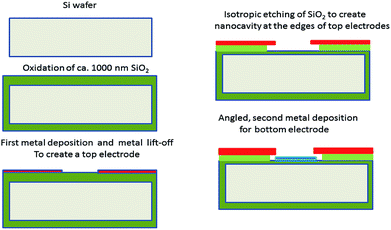
2. Fabrication of interdigitated nanogap electrodes as a chemocapacitor
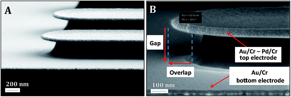
An overview and a cross section of the nanogap IDE are shown in Fig. 1. The nanogap IDE has a patterned area of 1 mm × 1 mm, consisting of 250 top finger electrodes and 250 bottom finger electrodes. Each finger electrode has a width and length of 2 μm and 1000 μm, respectively. A distance (the gap) from top to bottom electrodes is determined by an etching depth of a sacrificial SiO2 layer, and a thickness of the bottom electrode. The process steps of the nanogap IDEs are shown in Fig. 2, and are as follows: a 4-inch {100}-Si is coated with 1000 nm of wet-thermal silicon dioxide (SiO2), followed by microlithography, a metal deposition and a metal lift-off to form the top finger electrode array. The top electrodes are layers of ca. 30 nm palladium (Pd) and 5 nm adhesive chromium (Cr).
 |
| | Fig. 1 An overview of the interdigitated nanogap electrodes – (A). A cross section (over C–C) of one bottom electrode and its two adjacent top electrodes, showing the nano gaps across the finger electrodes – (B). | |
 |
| | Fig. 2 Fabrication process of an interdigitated nanogap electrodes (nanogap IDEs). | |
Afterwards, the SiO2 is partially and isotropically etched using buffered hydrofluoric acid (BHF; 1:7) to create a nanocavity at the edges of the top electrodes. Next a thin-film evaporation under an angle is carried out to deposit ca. 30 nm of gold (Au) layer on to the substrate and into the nanocavity to create the second electrodes of the nanogap IDEs. Also, 5 nm of Cr is used as the adhesive layer for this Au deposition step. In our work, all the metal depositions are carried out using an E-beam evaporator technique with a typical metal evaporation rate of ca. 1 Å s−1.29
Fig. 3 shows SEM images of the fabricated nanogap IDEs. It can be seen that the top and bottom electrodes are separated with a gap of ca. 250 nm, and an overlap of the top and bottom electrodes form a capacitor. Note that to form the nanogap IDEs capacitor no nanolithography is required and only conventional micro-fabrication is applied.
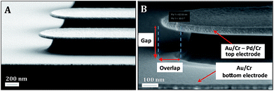 |
| | Fig. 3 An overview SEM image of several electrodes of the nanogap IDEs on silicon chip – (A). SEM image shows top and bottom electrodes and its overlap that creates a capacitor – (B). | |
3. Polymer coating of nanogap IDEs
PVPH was dissolved in ethanol by sonication for several minutes until a clear polymer solution was obtained. Nanogap IDEs as nanogap capacitors were coated with polymer by dipping them slowly into the polymer solution, with the electrodes in a vertical position, until the liquid reached the bottom of the electrodes. The chip was held in this position until the gaps between the electrodes were filled with polymer solution by capillary action.
This took less than a minute and filling of the gaps could be observed by a changing reflection of light. When the gaps had been completely filled, the chip was submerged in the polymer solution completely, after which the chip was spin coated at 3000 rpm for 2 minutes to form a thin layer. Finally, the sample was annealed at 60 °C overnight. Moreover, in order to further investigate the effects of sensing materials towards sensitivity of nanogap IDEs, in these experiments, we used same type of Si–NH2 NPs as prepared in our previous work published elsewhere28 with concentration of 1 wt% in a solution of PVPH 10 wt% in ethanol to create a polymer solution with nanoparticles (NPs).
4. Acetone gas sensing setup
An experimental Signal Measurement System (SMS) was used to characterize the behavior of the nanogap IDE in a clean air atmosphere. The SMS is shown in Fig. 4. The humidity, measured with a calibrated AHT-200-01 sensor (Ohmic Industries), in the volume controlled chamber (8.3 liter) is PC regulated with high speed inlet and exhaust valves running through, or by passing, a bubbler. The selected humidity sensor is a thermal conductivity type. This sensor is capable of measuring in an environment with volatile chemicals such as ketones. A downside of this sensor type is that it does require a temperature compensation of the output data and this task is programmed and operated by the PC controller. The temperature in the chamber is regulated with a Peltier element, a heat sink and a fan both inside and outside the SMS. Overpressure is regulated with an exhaust valve monitored and recorded with a pressure transducer. When the internal pressure exceeds ambient levels the exhaust valve will open until the pressure relaxes to ambient level.
 |
| | Fig. 4 Setup of the signal measurement system for sensing acetone concentrations. | |
A bubbler with a diluted acetone concentration also controlled by a high-speed valve was used to insert acetone. The concentration in the system was measured using a calibrated PID-AH sensor (alpha sense), capable of sensing a range from 0.1 ppm to 6000 ppm of acetone. The output of this reference sensor was fed into a calibrated DMM operating under PC control. The data of this reference sensor was used in a software feedback loop of the SMS. The nanogap IDEs capacitor value was measured at roughly 2 MHz depending on the nanogap IDEs capacitance, using the Texas Instruments FCD2212. This semiconductor was placed on an experimental measurement PCB clip, directly next to the pogo pins that connect to the nanogap IDEs under test. The FDC2212 offers a 300 aF resolution with 168 dB dynamic range and, was interfaced to the control PC with a Micro Controller Unit (MCU) and programmed to deliver new readout values on command. The control PC executes a script file, used for setting the wanted, temperature, humidity and acetone concentration, values in the SMS. Every line in the script file triggers a read command of all reference sensors and experimental nanogap IDEs capacitor value and both wanted and current values are stored in an Excel file structure for further analysis. With the script file, measurements can be designed and repeated as chosen, using the same timing and variable settings in the SMS.
5. Finite element analysis of nanogap IDEs as a capacitor
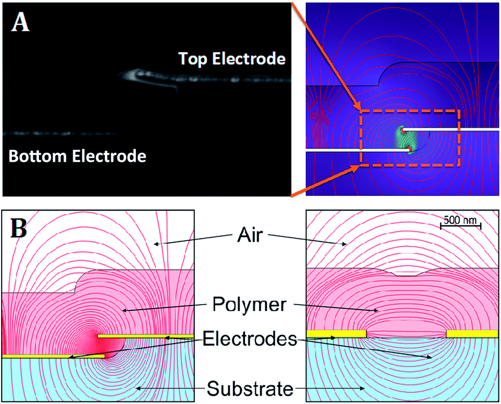
The presence of analytes in the sensing layer induces a change in the dielectric constant. This change is measured as a change in the capacitance value of the nanogap IDE. The greater the change in capacitance relative to the total capacitance of the system, the more sensitive the sensor is. Modelling can give insight into factors maximizing signal and minimizing parasitic capacitance.30 Analytical prediction of capacitance is often complex, because electric fields extend into substrates and different media.31–33 Also, analytical models are usually only correct for specific geometries not relevant in this case.34 Therefore, we used finite element analysis using COMSOL Multiphysics 5.2 (COMSOL Inc., Burlington MA, USA) to show the effect of two electrode designs: a rectangular electrode array with a micro-gap as used in previous experiments,28 and the rectangular electrode array with a nanogap introduced in this paper. In both designs a polymer coating of 800 nm was applied. Parametric sweeps of geometrical and material parameters were performed. As the complete chip geometry requires considerable computing power to model, these simplified models were studied to gain approximations of the expected electric field and capacitance.
From theory, it has been known that electric fields are highest near regions of conductors with small radius of curvature as a consequence of the high local charge density.35,36 Closer to these regions, more charge can be stored as the dielectric is more strongly polarized.37 Therefore, it can be concluded that protruding parts of the geometry, like electrode edges, contribute most to the capacitance of the system. Furthermore, many simplified nanogap IDE models predict that the so called fringe capacitance is more significant when the electrodes are placed more closely together.32,38 This implies that the sensing layer may be made be thicker to include interactions with the electric field and fluctuations of the capacitance further away from the electrodes.25 However, this perception is only valid for electrodes for which the separation is much larger than the electrode thickness, which does not hold for the design discussed in this work. For our design, the field in between the upper and lower electrode surfaces dominates the field outside as shown in Fig. 5. Therefore, the thickness of the polymer layer on top of the electrodes is not expected to influence the response of the sensor significantly. From COMSOL simulations, it became apparent that the electric field in a nanogap capacitor is much stronger than that of a typical IDE in comparable circumstances (voltage, polymer thickness, substrate thickness).23,24,30
 |
| | Fig. 5 A cross-sectional SEM image of a nanogap (A – left) and its electric field line distributions as calculated by COMSOL (with illustrative overlay) (A – right). Capacitors are composed of two electrodes covered in a polymer film, supported by silicon nitride, in air environment. A typical nanogap capacitor (250 nm vertical spacing, 130 nm horizontal overlap, 800 nm polymer thickness) (B – left). A typical nano-IDE (10 μm × 0.1 μm × length, 1 μm spacing) (B – right). The field line density is indicative of the electric field strength. | |
The maximum electric field strength of a nanogap IDEs was calculated to be 4.47 times higher. Furthermore, the field does not extend quite as far into the substrate in case of nanogap IDEs. This implies that the sensing layer can be thinner and therefore more responsive to changes in the environment. For the geometries discussed here, an arbitrary change in dielectric constant of the polymer yields a relative change in simulated capacitance that is 3.14 times lower for the micro-IDE, see Fig. 6. Compared to a planar IDE having electrodes with similar dimensions (250 nm spacing, 2 μm width), the field of a nanogap IDEs is 3.68 times higher and the simulated sensitivity is 1.64 times better.
 |
| | Fig. 6 Simulated sensitivity of a typical micro IDE and a nanogap capacitor with a planar geometry. An arbitrary change in permittivity of the polymer yields a much larger relative change in capacitance in a two dimensional geometry. | |
Results and discussion
1. Signal processing
In our set-up, four variables are measured by separate sensors: the capacitance of the chip, humidity, temperature and the acetone concentration in the measurement chamber. Fig. 7A shows some typical values during an acetone sensing experiment. The temperature of the system is kept constant within 0.05 °C and the humidity within 0.4% RH. The humidity inside the measurement chamber decreases when acetone is introduced, due to the hygroscopic nature of this vapor, which leads to additional adjustment of the humidity level. Furthermore, there is a strong correlation between the measured capacitance of the nanogap IDEs and the humidity of the system: peaks in the humidity signal coincide with peaks in the capacitance signal. Thus, the nanogap IDEs responds to water. Measurements showed that there is in fact a linear relationship between humidity and measured capacitance at low concentrations (ESI. Fig. S1†), so that it is possible to correct for variations in humidity by subtracting the humidity signal from our detected capacitance (Fig. 7B). After application of a 10 point moving average filter, the capacitance signal follows the acetone concentration in the measurement concentration very well.
 |
| | Fig. 7 Measured signals in acetone sensing experiments: capacitance of the measured chip, humidity, temperature and acetone concentration – (A) and their signal processing – (B). | |
2. Sensitivity
In previous work, we presented an acetone sensor that consists of micro-gap IDEs coated with PVPH.28 With the same mechanism of acetone detection explained in our previous work, Fig. 8A shows the improvement in acetone sensitivity achieved by the new nanogap design. In this figure both chips were coated with a 2 μm thick PVPH layer. The acetone sensitivity increased from 0.028 fF ppm−1 for the micro-gap chip to 0.97 fF ppm−1 for the nanogap IDEs, a 35-fold increase. Fig. 8B shows that the sensitivity could be increased further by enlarging the size of the nanogap IDEs. Here, the increase in sensitivity scales linearly with the surface area on which the chip was prepared. Furthermore, it has been shown that the addition of Si–NH2 NPs to PVPH layer improves the sensitivity of the nanogap IDEs massively.28
 |
| | Fig. 8 Sensitivity towards acetone of several nanogap IDEs in comparison with micro-gap IDEs. Here, the change in capacitance (ΔC) that was measured with presence of acetone, is plotted as a function of acetone concentration. Difference between a micro-gap IDE and nanogap IDE coated with 2 μm PVPH. The inset shows the micro-gap signals in detail – (A). Nanogap IDE on surfaces of 1 mm2 and 3 mm2 coated with 1 μm PVPH with and without nanoparticles – (B). | |
3. Detection limit
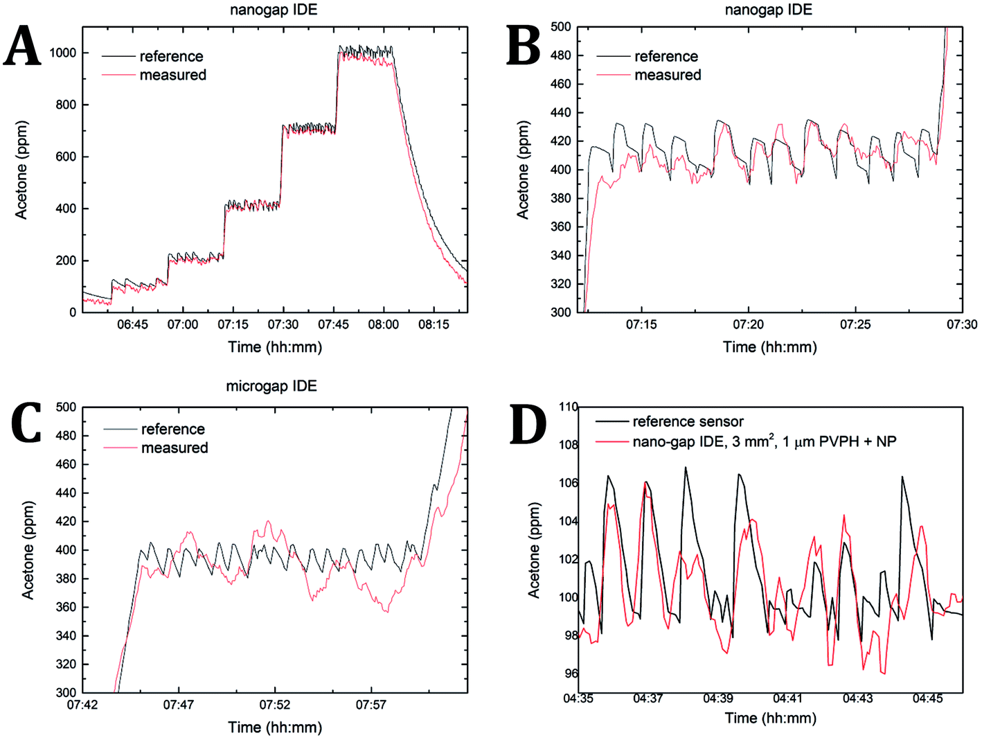
To determine the detection limit of the nanogap IDEs, we applied a step-function with different levels of acetone concentration (Fig. 9A). For high concentrations that are depicted in this graph, the measured signal follows the reference signal very well. However, to determine the detection limit of the nanogap IDEs, we need to measure at much lower acetone concentrations. Unfortunately, our set-up did not allow us to go below 100 ppm. Thus, to obtain information about the nanogap IDE's response towards smaller concentrations, we analyzed the small fluctuations in acetone concentration that appear at each step as a result of the system keeping the concentration at a certain level. Fig. 9B shows the response of a typical nanogap IDE to a 100 ppm steps. The measured signal follows even small steps very well (about 30 ppm in this case) and stays within 20 ppm from the reference signal. For comparison, Fig. 9C shows the response of a micro-gap IDEs towards similar step heights. It is clear that the response does not follow the small step responses detected by the reference sensor, while it stays within 50 ppm from the reference signal. So, even though the much higher responses towards acetone of the nanogap IDEs was accompanied by a higher level of noise, the nanogap IDEs did respond better to smaller levels in acetone concentration. The smallest changes of signal that were detected this way were 6 ppm peaks, obtained by a 3 mm2 nanogap IDEs coated with a 1 μm PVPH layer containing NPs (see Fig. 9D).
 |
| | Fig. 9 Details of measured nanogap IDEs chips and reference sensor responses to acetone. Step-function showing the response of a nanogap IDE coated with 1 μm PVPH towards different acetone levels – (A). Detail of (A) showing the acetone response in the 100 ppm step regime – (B). Response of comparable micro-gap IDE chip coated with 2 μm PVPH towards a 400 ppm step response – (C). Smallest detected peaks of 6 ppm detected by a 3 mm2 nanogap IDEs chip coated with 1 μm PVPH containing nanoparticles – (D). | |
4. Sensor properties: stability, response, recovery and durability
After fabrication the coated nanogap IDEs are stored in ambient air. Consequently, they are exposed to water vapor.
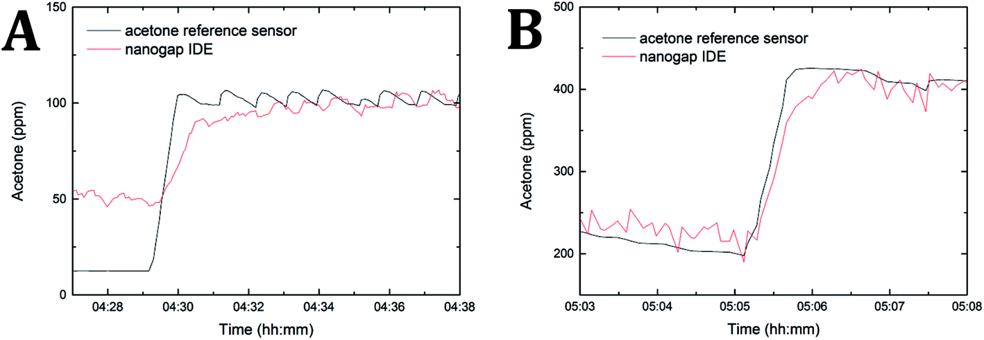
When acetone response is measured, the samples are in an environment of 15% RH, much lower than ambient air. Fig. 10A shows that the decay time of the capacitance signal due to adaptation to the humidity level is approximately 5 to 6 hours. This time is needed to remove all water from the polymer layer. While it takes a long time to remove all water from the polymer layer (due to hydrogen bonds within the polymer chains), the chip responds fast to small humidity changes that are caused by the system adjusting its humidity level (Fig. 10B). In fact, the chip responds even faster than our reference humidity sensor. The response time towards acetone was determined by looking in detail to 100 ppm and 200 ppm acetone steps (as presented in Fig. 9). For a nanogap IDEs capacitor coated with PVPH without nano-particles, the response of the nanogap IDEs occurs at the same time as that of the reference sensor. The response time is about 1 minute in this case, as can be seen in Fig. 11B. When nanoparticles are present in the PVPH layer, we find a different behavior. Meanwhile, Fig. 11A shows that the response of the sensor has a delay of about 20 seconds with respect to the reference sensor. This is clearest when looking at the small peaks between 04:32 and 04:34. The response time to 100 ppm acetone is about 4 minutes. Here the nanogap-IDE coated with PVPH containing nanoparticles responded with a delay and a longer response time than nanogap IDEs coated with PVPH only. As mentioned before, the nanogap IDEs containing nanoparticles are also more sensitive towards acetone and the lowest detection limit was reached using this type of coating. At present it is not clear how the nanoparticles improve the sensitivity of the IDE, and why the improved sensitivity goes together with a delay in response towards acetone, and a longer response time than when no nanoparticles are used. The decaying baseline, visible in Fig. 10A, can be subtracted from these data, to prove that the response is equally high for every peak. Fig. 12 shows the results for repeated 100 ppm acetone peaks. We find a response of 1.2 pF for every 100 ppm peak.
 |
| | Fig. 10 Stabilization of a 3 mm2 nanogap-IDE coated with 1 μm of PVPH containing nanoparticles. In black the response of the nanogap IDEs to subsequently a 100 ppm and 1000 ppm acetone peak, in red the fitted exponential with a decay time of 5 hours (A). Overlay of signals from the reference humidity sensor (in black) and a nanogap IDEs (in red) while no acetone is present (B). Here, the nanogap IDEs respond faster to small humidity peaks. | |
 |
| | Fig. 11 Response time of nanogap-IDE coated with 1 μm PVPH with (A) and without nanoparticles (B). | |
 |
| | Fig. 12 Repeated 100 ppm acetone peaks detected by a reference sensor (top) and nanogap IDEs (bottom). | |
Conclusions
In summary, we have designed micro and nano IDE capacitor structures featuring up to a 35 times improved sensitivity compared to microgap IDEs based on our previous work. Sensitivity could be further enhanced by increasing the area on which the nanogap IDEs structure was fabricated. The best performing nanogap IDE, coated with PVPH containing nanoparticles, had a response time of several minutes. This type of nanogap IDE could detect changes of response signal down to 6 ppm. The sensor could be used multiple times, as proven by long term repeatability studies. Since the desired material is homogenously coated in between the nanogaps, a robust electric field connection between these nanogaps can be assured to easily detect a very small amount of analyte. Our approach can also create addressable high-density nanogap electrodes in large scale by conventional micro-fabrication process. By simply changing the active layers into specific advanced materials such as non-conductive polymers or nano-composite, a new generation of nanogap devices is promising to detect a large range of analytes.
Conflicts of interest
There are no conflicts to declare.
Acknowledgements
This work is supported by NanoNextNL (10A.05), a micro and nanotechnology consortium of the Government of the Netherlands and 130 partners.
References
- V. P. Menon and C. R. Martin, Anal. Chem., 1995, 67, 1920–1928 CrossRef CAS.
- I. V. Sapkov and E. S. Soldatov, 2013, 8700, 87000O.
- D. R. Ward, F. Huser, F. Pauly, J. C. Cuevas and D. Natelson, Nat. Nanotechnol., 2010, 5, 732–736 CrossRef CAS PubMed.
- S.-K. Kim and J.-Y. Son, Electrochem. Solid-State Lett., 2009, 12, J17–J19 CrossRef CAS.
- M. Löhndorf, U. Schlecht, T. M. A. Gronewold, A. Malavé and M. Tewes, Appl. Phys. Lett., 2005, 87, 1–3 CrossRef.
- M. A. Reed, C. Zhou, C. J. Muller, T. P. Burgin and J. M. Tour, Science, 1997, 278, 252–254 CrossRef CAS.
- H. Park, J. Park, A. K. L. Lim, E. H. Anderson, A. P. Alivisatos and P. L. McEuen, Nature, 2000, 407, 57–60 CrossRef PubMed.
- K. Liu, P. Avouris, J. Bucchignano, R. Martel, S. Sun and J. Michl, Appl. Phys. Lett., 2002, 80, 865–867 CrossRef CAS.
- H. Zhang, S.-W. Chung and C. A. Mirkin, Nano Lett., 2003, 3, 43–45 CrossRef CAS.
- A. C. Whalley, M. L. Steigerwald, X. Guo and C. Nuckolls, J. Am. Chem. Soc., 2007, 129, 12590–12591 CrossRef CAS PubMed.
- X. Guo, A. Whalley, J. E. Klare, L. Huang, S. O'Brien, M. Steigerwald and C. Nuckolls, Nano Lett., 2007, 7, 1119–1122 CrossRef CAS PubMed.
- C. P. R. Dockendorf, D. Poulikakos, G. Hwang, B. J. Nelson and C. P. Grigoropoulos, Appl. Phys. Lett., 2007, 91, 243118 CrossRef.
- J. Tamaki, A. Miyaji, J. Niimi, Y. Nakataya and S. Konishi, IEEJ Trans. Sensors Micromachines, 2006, 126, 573–577 CrossRef.
- T. Chang, H. Jung, B. Jang, J. Lee, J.-S. Noh and W. Lee, Sens. Actuators, A, 2013, 192, 140–144 CrossRef CAS.
- S. Mubeen, B. Yoo and N. V. Myung, Appl. Phys. Lett., 2008, 93, 133111 CrossRef.
- B. Jang, K. Y. Lee, J.-S. Noh and W. Lee, Sens. Actuators, B, 2014, 193, 530–535 CrossRef CAS.
- E. Menumerov, B. A. Marks, D. A. Dikin, F. X. Lee, R. D. Winslow, S. Guru, D. Sil, E. Borguet, P. Hutapea, R. A. Hughes and S. Neretina, ACS Sens., 2016, 1, 73–80 CrossRef CAS.
- F. Favier, 2012 IEEE Sensors, 2012, 1–4 Search PubMed.
- E. Lee, J. Lee, J.-S. Noh, W. Kim, T. Lee, S. Maeng and W. Lee, Int. J. Hydrogen Energy, 2012, 37, 14702–14706 CrossRef CAS.
- C. Shi, H. Qin, L. Li, Y. Chen, L. Ju and J. Hu, Appl. Surf. Sci., 2015, 327, 168–173 CrossRef CAS.
- K. Muthukrishnan, M. Vanaraja, S. Boomadevi, R. K. Karn, V. Singh, P. K. Singh and K. Pandiyan, J. Alloys Compd., 2016, 673, 138–143 CrossRef CAS.
- F. S. Dias, L. G. Tartuci, H. d. F. Gorgulho and W. S. Machado, Sens. Actuators, B, 2016, 231, 440–449 CrossRef CAS.
- M. Kahali Moghaddam, A. Breede, A. Chaloupka, A. Bödecker, C. Habben, E.-M. Meyer, C. Brauner and W. Lang, Sens. Actuators, A, 2016, 243, 123–133 CrossRef CAS.
- O. Laczka, E. Baldrich, F. X. Muñoz and F. J. del Campo, Anal. Chem., 2008, 80, 7239–7247 CrossRef CAS PubMed.
- H. Omran and K. N. Salama, IEEE 3rd Int. Conf. Smart Instrumentation, Meas. Appl., 2015 Search PubMed.
- H. Xie, Q. Yang, X. Sun, J. Yang and Y. Huang, Sens. Actuators, B, 2006, 113, 887–891 CrossRef CAS.
- Z. Ying, Y. Jiang, X. Du, G. Xie, J. Yu and H. Tai, Eur. Polym. J., 2008, 44, 1157–1164 CrossRef CAS.
- Q. Nguyen Minh, A. Kuijk, S. P. Pujari, F. van de Bent, J. Baggerman, H. D. Tong, H. Zuilhof and C. J. M. van Rijn, Sens. Actuators, B, 2017, 252, 1098–1104 CrossRef.
- D. H. Tong, P. D. Tran, X. T. T. Pham, V. B. Pham, T. T. T. Le, M. C. Dang and C. J. M. van Rijn, Adv. Nat. Sci.: Nanosci. Nanotechnol., 2010, 1, 15011 CrossRef.
- P. Oikonomou, G. P. Patsis, A. Botsialas, K. Manoli, D. Goustouridis, N. A. Pantazis, A. Kavadias, E. Valamontes, T. Ganetsos, M. Sanopoulou and I. Raptis, Microelectron. Eng., 2011, 88, 2359–2363 CrossRef CAS.
- R. Igreja and C. J. Dias, Sens. Actuators, A, 2004, 112, 291–301 CrossRef CAS.
- H. Hammer, J. Microelectromech. Syst., 2010, 19, 175–182 CrossRef.
- S. Gevorgian, E. Carlsson, S. Rudner, L. D. Wernlund, X. Wang and U. Helmersson, IEE Proc. Microwaves Antenn. Propag., 1996, 143, 397–401 CrossRef.
- R. Igreja and C. J. Dias, Sens. Actuators, A, 2011, 172, 392–399 CrossRef CAS.
- N. G. Green, A. Ramos and H. Morgan, J. Electrost., 2002, 56, 235–254 CrossRef.
- H.-W. Jung, Y. W. Chang, G. Lee, S. Cho, M.-J. Kang and J.-C. Pyun, Anal. Chim. Acta, 2014, 844, 27–34 CrossRef CAS PubMed.
- R. B. Bird, AIChE J., 1964, 10, 794 CrossRef.
- H. Jayatilleka, W. D. Sacher and J. K. S. Poon, IEEE Photonics J., 2013, 5, 2200211 CrossRef.
Footnote |
| † Electronic supplementary information (ESI) available. See DOI: 10.1039/c7ra09441h |
|
| This journal is © The Royal Society of Chemistry 2017 |
Click here to see how this site uses Cookies. View our privacy policy here. 
 Open Access Article
 This Open Access Article is licensed under a
  af and
C. J. M. van Rijn
af and
C. J. M. van Rijn