
 Open Access Article
 This Open Access Article is licensed under a
 Creative Commons Attribution 3.0 Unported Licence
Indium-doped ZnO horizontal nanorods for high on-current field effect transistors
Ziqiang Zhu ab,
Borui Lib,
Jian Wenb,
Zhao Chenb,
Zhiliang Chenb,
Ranran Zhanga,
Shuangli Yea,
Guojia Fang*b and
Jun Qian*a
ab,
Borui Lib,
Jian Wenb,
Zhao Chenb,
Zhiliang Chenb,
Ranran Zhanga,
Shuangli Yea,
Guojia Fang*b and
Jun Qian*a
aSchool of Printing and Packaging, Wuhan University, Wuhan, 430072, P. R. China. E-mail: whuqianjun@163.com
bSchool of Physics and Technology, Wuhan University, Wuhan, 430072, P. R. China
First published on 1st December 2017
Abstract
High on-current field effect transistors (FETs) are highly desirable for driving information displays such as active matrix organic light-emitting diode displays. Herein, indium-doped ZnO (IZO) horizontal nanorod arrays were fabricated for high on-current FETs by a facile and tunable hydrothermal method. We have found that indium doping can influence the growth behavior of ZnO nanorods. After indium doping, the ZnO nanorods tend to grow better along the horizontal direction and have a better flat morphology. More importantly, indium doping increases the carrier concentration of the IZO nanorods; this leads to better transfer and output performances of the IZO nanorod FETs. Therefore, the IZO nanorod FET with a high on-current of 6.39 × 10⁻⁴ A and a field effect mobility of 26.3 cm2 V−1 s−1 has been synthesized and demonstrated in this study.
1. Introduction
In the past few decades, ZnO nanorods have attracted significant attention1 because of their unique photoelectrical properties2–6 such as wide direct band-gap (3.37 eV), electron transport confinement, and tunable electrical property by doping.7–11 Therefore, they have been applied in ultraviolet photodetectors,12–16 field electron emission displays,17 and field effect transistors (FETs).18–20 Hydrothermally grown ZnO nanorods have been used in FETs because of their low temperature growth, tunable growth behavior, and electrical property.21,22 However, generally, ZnO nanorod FETs exhibit the problem of low on-current, which affects their practical applications. Some efforts have been made to increase the on-current of lateral ZnO nanorod FETs, which mainly include two aspects: (1) optimization of horizontal ZnO nanorod growth between electrodes without vertical growth or radial growth, better contact to gate dielectrics, and better contact with ZnO nanorods and (2) increase of the ZnO nanorod number and better alignment of ZnO nanorods between source and drain electrodes.21–27 Researchers have made some progress in the optimization of ZnO nanorod growth behavior using a more effective passivation electrode and complex processing method.23,28 However, the ZnO nanorod FETs obtained usually have a low on-current of μA. A smart structure has been designed for alignment of a greater number of ZnO nanorods between the source and drain electrodes;27 however, it is not convenient for integration. Doping is an effective way to increase the carrier concentration of semiconductors; however, to the best of our knowledge, it has not been used for on-current enhancement of horizontal ZnO nanorod FETs.In this study, we have chosen indium doping for on-current enhancement of ZnO nanorod FETs because indium has an ionic radius similar to that of zinc and is less prone to oxidation.29–33 Interestingly, we found that In doping could influence the growth behavior of ZnO nanorods to some degree. Scanning electron microscopy (SEM) and transmission electron microscopy (TEM) analysis illustrate that indium doping benefits the horizontal growth of ZnO nanorods and results in a better flat morphology. The energy dispersive spectroscopy (EDS) and X-ray photoelectron spectroscopy (XPS) analysis illustrate the presence of indium element in the ZnO nanorod samples. Electrical property measurement suggests that FETs obtained from indium-doped ZnO (IZO) nanorods have better performance than those obtained from undoped ZnO nanorods. The IZO nanorod FETs show a high on-current of 6.39 × 10⁻⁴ A and a field effect mobility of 26.3 cm2 V−1 s−1.
2. Experimental details
For better comparison, FETs with both ZnO and IZO horizontal nanorods were synthesized under the same conditions. An n+-Si (resistivity ∼ 0.02 Ω cm) wafer with a 240 nm SiO2 layer was used as the starting substrate. The cut pieces were ultrasonically cleaned with acetone, ethanol, and deionized water, in sequence, and then dried using N2 gas. Photolithography was performed for defining the channel patterns of 5 μm length and 50 μm width. A 300 nm thick ZnO seed layer was deposited on the SiO2 substrate using a radio frequency magnetron sputtering deposition system, and then, a 70 nm thick tin-doped indium oxide (ITO) passivation layer was deposited. After a lift-off process with acetone, the patterned device structures of ITO (70 nm)/ZnO (300 nm) on SiO2/Si substrates were obtained. For the hydrothermal process, an aqueous solution of zinc nitrate hexahydrate (Zn(NO3)2·6H2O, 0.0025 M) and equimolar hexamethylenetetramine (HMTA, 0.0025 M) was prepared, and the substrates were suspended upside down in the solution. The ZnO nanorod growth was performed in a sealed reaction vessel at 85 °C for 12 h. For the IZO nanorod growth, the indium chloride tetrahydrate (InCl3·4H2O) with a doping concentration of 2 at% was added to the solution. All the reagents used in this synthesis were of analytical grade and used as-received without further purification. After the hydrothermal reaction, the fabricated samples were removed from the solution, rinsed with distilled water, and dried in an oven at 60 °C for 2 h. Then, the FETs composed of horizontally aligned ZnO or IZO nanorods were obtained. The fabrication processes are illustrated in Fig. 1(a).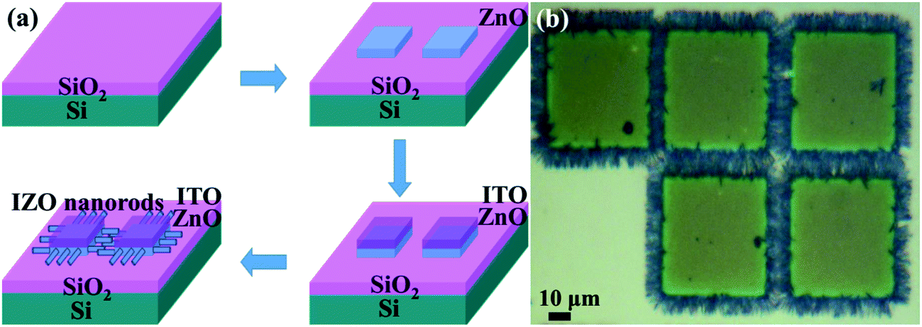 | ||
| Fig. 1 (a) Schematic of the fabrication process and (b) optical image of the IZO nanorod FETs. | ||
The growth morphologies and alignments of ZnO and IZO nanorods between source and drain electrodes were characterized using an SEM (Hitachi S-4800). The crystal property of the IZO nanorods was characterized using a TEM (JEM-2100). The crystal structure and growth orientation of the ZnO and IZO nanorods were characterized by an XRD (Bruker D8). The chemical composition of the IZO nanorod sample was characterized by an EDS analysis. The chemical bonding structures of ZnO and IZO nanorods were analyzed using an XPS (Thermo Scientific Escalab 250Xi). The electrical property of the ZnO and IZO nanorod FETs was characterized by measuring their transfer and output characteristics using a Keithley 4200 system.
3. Results and discussion
The schematic of the fabrication process of ZnO and IZO nanorod FETs is shown in Fig. 1(a). The in situ hydrothermal growth of ZnO nanorods proceeds with the ZnO seed layer and ITO passivation layer. The in situ hydrothermal growth of IZO nanorods proceeds under the same conditions, but with the In dopants in the solution. When grown between two square electrodes, the IZO nanorods assemble to form an FET. A representative optical image of the IZO nanorod array FETs is shown in Fig. 1(b). The IZO nanorods were uniformly grown and arranged well between electrodes.Interestingly, In doping affects the growth behavior, including morphology and growth direction, of the ZnO nanorods, as shown in Fig. 2(a)–(f). Before In doping, the ZnO nanorods show a typical hexagonal prism morphology, which grow along both the horizontal and vertical directions. However, after In doping, the IZO nanorods show a belt morphology, which only grows along the horizontal direction. Moreover, different In doping contents affect the growth behavior of the ZnO nanorods. When the In doping content changes from 0.5 at% to 2 at%, the bottom layer IZO nanorods sufficiently grow, but the top layer IZO nanorods gradually approach sufficient growth with an increase in the doping content. When the In doping content increases to 5 at%, the arrangement begins to disperse. The In doping changes the surface energy of the IZO nanorods and affects the IZO nanorod growth to some degree. When the In doping content increases to 10 at%, only sporadic IZO nanorods stretch out; this is probably attributed to the difficulty in increasing the nucleation and growth on the ZnO seed layer. Based on better growth along the horizontal direction and better belt morphology, we choose 2 at% In doping content to fabricate IZO nanorod FETs in this study. The variation of growth behavior of IZO nanorods is beneficial for better contact with dielectrics and electrodes and carrier transport performance enhancement, which may result in electrical performance improvement of the IZO nanorod FETs.
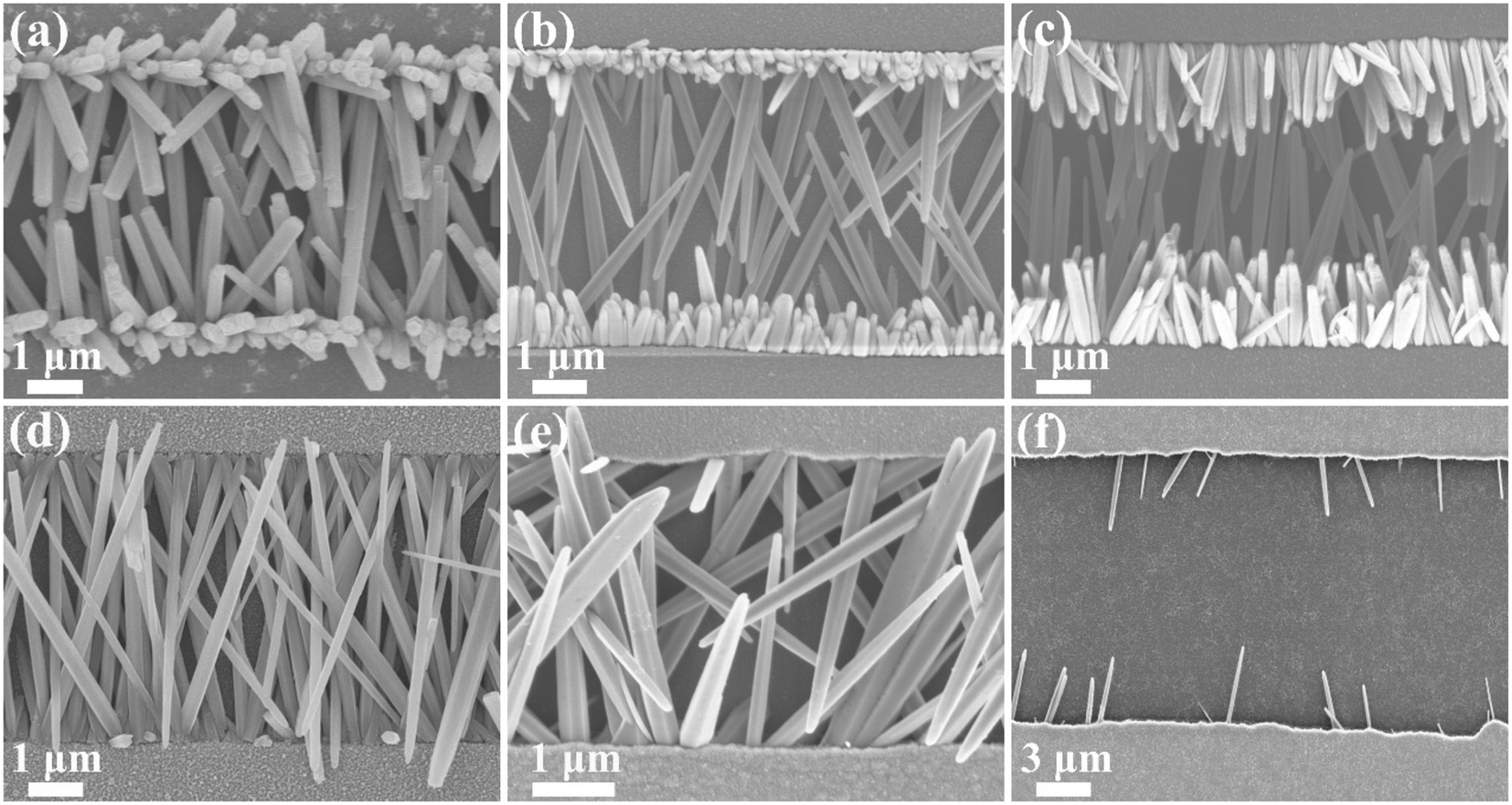 | ||
| Fig. 2 SEM images of (a) undoped ZnO, (b) 0.5 at%, (c) 1 at%, (d) 2 at%, (e) 5 at%, and (f) 10 at% In-doped ZnO nanorods. | ||
For further observation, a high resolution transmission electron microscopy (HRTEM) image of the IZO nanorod is shown in Fig. 3(a). In the low magnification TEM image for the IZO nanorods in the inset of Fig. 3(a), we can find that the IZO nanorods show a belt morphology rather than the typical ZnO hexagonal prism morphology; this can be ascribed to the surface energy change of IZO nanorods with In doping. The wave-like edge could be ascribed to the instability of crystallization and etching on the surface of IZO nanorods in the reaction solution. The growth direction is along the c-axis (001) direction. The lattice spacing along the (001) direction is 0.52 nm, corresponding to the lattice constant c of the ZnO crystal. The selected area electron diffraction (SAED) image is shown in Fig. 3(b), suggesting the same abovementioned observation. The crystal property of the ZnO and IZO nanorods was characterized by XRD. As shown in Fig. 4, both the ZnO and IZO nanorods only show a strong characteristic peak of the (002) plane of the ZnO wurtzite structure. The peak position does not change after indium doping. We conclude that highly oriented nanorod arrays have been synthesized for both pure ZnO and indium-doped ZnO nanorod situations.
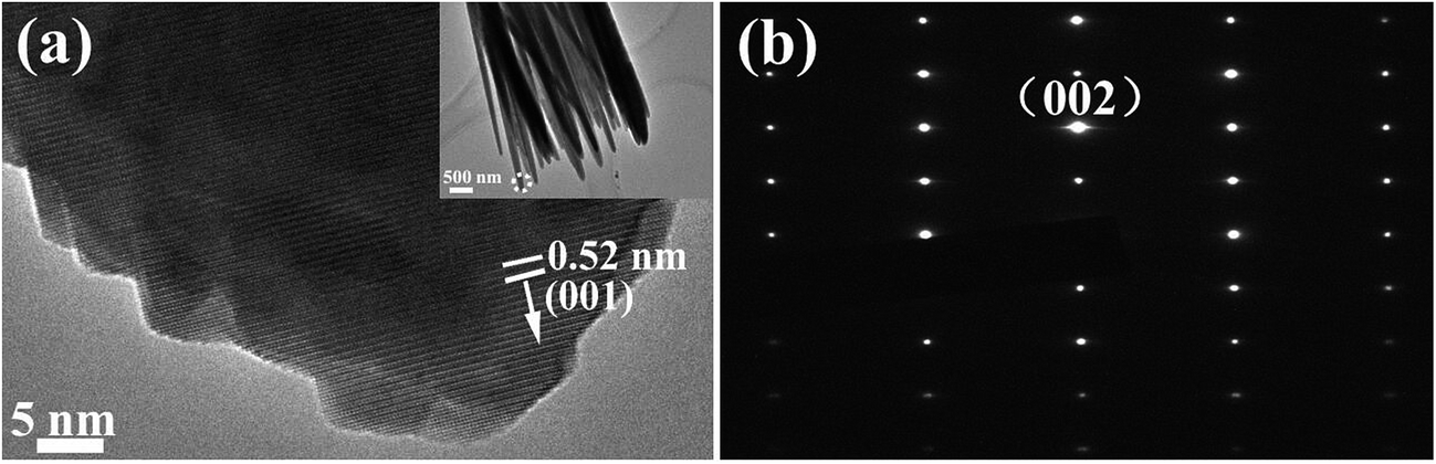 | ||
| Fig. 3 (a) An HRTEM image of the IZO nanorod (the inset shows a low magnification image of the IZO nanorods), and (b) a SAED image of the IZO nanorod. | ||
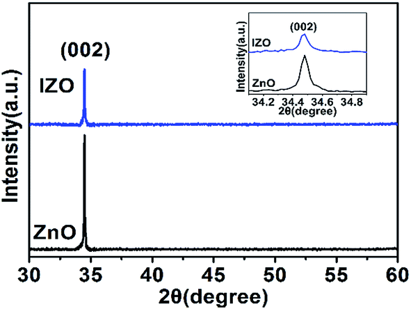 | ||
| Fig. 4 XRD patterns of the ZnO and IZO nanorods on the ZnO seed layer. | ||
Fig. 5(a) shows the EDS spectrum of the IZO nanorods. Besides Zn, O, and Si peaks, an In peak was found. The indium content in IZO is about 0.45 at%. The EDS spectrum shows that In is doped into the ZnO nanorods. Based on the EDS element mapping analysis of the IZO nanorod, as shown in Fig. 5(b), we can find only sporadic In element distribution in the nanorod.
 | ||
| Fig. 5 (a) EDS spectrum and (b) EDS element mapping analysis of the IZO nanorod. | ||
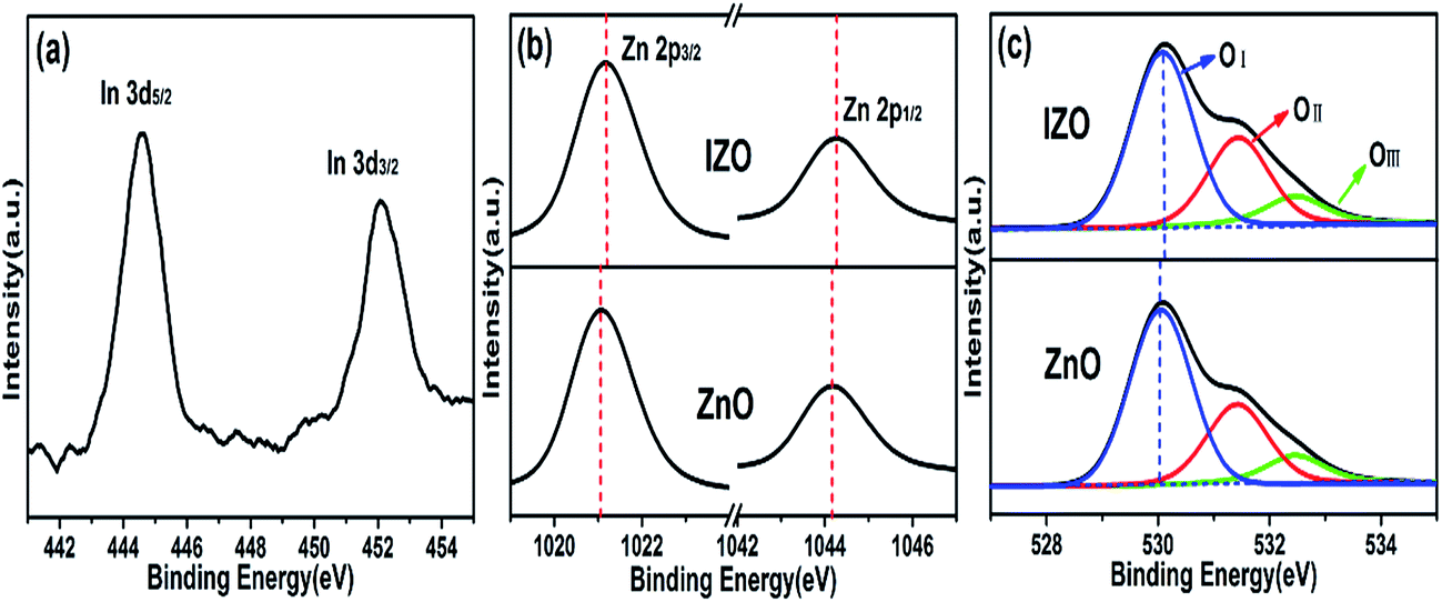
To further confirm the doping of indium into IZO nanorods, XPS analysis was performed. The In 3d spectrum of IZO nanorods is shown in Fig. 6(a). The appearance of the In spectrum and the absence of the In2O3 phase in the previous XRD patterns suggest that In element is doped into the ZnO crystal. In addition, compared to the ZnO nanorod sample, the Zn 2p3/2 and Zn 2p1/2 peaks of IZO nanorods shift slightly towards a higher binding energy (as shown in Fig. 6(b)). The peak shifts can be explained by the difference in the electronegativity of In (χ = 1.78) and Zn (χ = 1.65). Because of the higher electronegativity of In than that of Zn, the valence electron density of Zn in the Zn–O–In bond in the IZO nanorod sample becomes lower than that in the Zn–O–Zn bond in the ZnO nanorod sample. Consequently, the screening effect of Zn in the IZO nanorod sample is weakened, and the binding energy of Zn 2p increases. The O 1s deconvoluted spectra of the ZnO and IZO nanorods are shown in Fig. 6(c). The low binding energy peak (OI) corresponds to O2− combined with metal ions in the ZnO and IZO crystals. The medium binding energy peak (OII) is related to the oxygen deficiency in the ZnO and IZO nanorods crystals, indicating the corresponding oxygen vacancy concentration. The high binding energy peak (OIII) is ascribed to some chemisorbed oxygen components such as –CO3 and H2O. We can find that the O 1s peak of the IZO nanorods also shifts slightly towards a higher binding energy as compared to that of the undoped ZnO nanorod sample. The shift is due to the higher electronegativity of In ion than that of Zn ion, as abovementioned. An intensity ratio of OII/Ototal is obtained to compare the relative concentration of the oxygen vacancies: the values are 0.29 and 0.31 for the ZnO and IZO nanorod samples, respectively. The IZO nanorod sample with a higher value has more oxygen vacancies than ZnO because of the lower bond strength of In–O as compared to that of Zn–O. On the basis of the abovementioned analysis results, the In element is doped into the ZnO crystal, which would generate more oxygen vacancies; therefore, a higher carrier concentration can be obtained for the IZO nanorod arrays.
 | ||
| Fig. 6 XPS spectra of the ZnO and IZO nanorods corresponding to (a) In 3d, (b) Zn 2p, and (c) O 1s. | ||
The transfer characteristic curve of the ZnO nanorod FETs is shown in Fig. 7(a). The ZnO nanorod FETs can be well controlled by the gate voltage and exhibit a typical n-type transistor behavior. The field effect mobility of the horizontal nanorod array FETs is approximately calculated by μFE = Lgm/WCiVds. The mobility obtained from the ZnO nanorod array FET is 1.06 cm2 V−1 s−1, and the on/off ratio is 103. The on-current of ZnO nanorod FETs is 1.86 × 10⁻⁵ A at Vgs = 60 V and Vds = 5 V, which cannot meet practical requirement and still needs to be improved. The threshold voltage of the ZnO nanorod FETs is 10.99 V. The output characteristics curve of the ZnO nanorod FETs in Fig. 7(b) shows a distinct linear region, and there is no saturation current region when Vds is swept from 0 to 10 V and Vgs varies from 0 to 60 V with a 10 V per step. After In doping, the electrical property variation of the nanorod FETs is shown in Fig. 7(c) and (d). When the Vgs varies from −40 V to −60 V, there is an upward trend, as shown in Fig. 7(c). This could be due to the formation of an inversion channel. The mobility obtained from the IZO nanorod array FETs is 26.3 cm2 V−1 s−1, and the on/off ratio is 103. The on-current of IZO nanorod FETs is 6.39 × 10⁻⁴ A at Vgs = 60 V and Vds = 5 V, which has been enhanced by an order of magnitude because of slight In doping. The threshold voltage of IZO nanorod FETs is −3.32 V, which is decreased as compared to that of the ZnO nanorod FETs. The output characteristic curve of the IZO nanorod FETs in Fig. 7(d) shows a current–voltage behavior similar to that of ZnO nanorod FETs, but the Ids of IZO nanorod FETs is larger than that of the ZnO nanorod FETs. The characteristic parameters of ZnO and IZO nanorod FETs are summarized in Table 1. As a result, the In doping could increase oxygen vacancy concentration, carrier concentration, and field effect mobility. The FET source–drain current has been enhanced to quite a high level because of In doping. The IZO horizontal nanorod array FETs may have potential applications for future large current power devices.
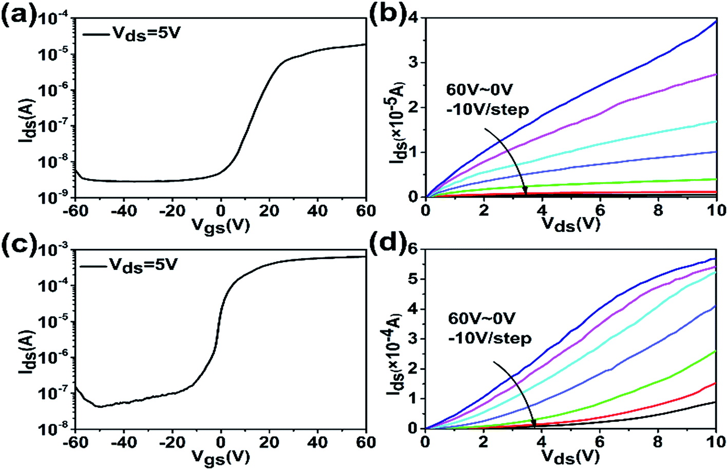 | ||
| Fig. 7 (a) Transfer characteristic and (b) output characteristic of the ZnO nanorod FETs. (c) Transfer characteristic and (d) output characteristic of the IZO nanorod FETs. The measurements were conducted under the same conditions as shown in the figure. | ||
| μ (cm2 V−1 s−1) | Vth (V) | On/off ratio | On-current (A) | |
|---|---|---|---|---|
| ZnO | 1.06 | 10.99 | 103 | 1.86 × 10⁻⁵ |
| IZO | 26.3 | −3.32 | 103 | 6.39 × 10⁻⁴ |
4. Conclusions
In summary, we have successfully fabricated horizontally grown IZO nanorod arrays and the corresponding FETs by a simple hydrothermal method. EDS and XPS analyses illustrate that there is In element in the nanorod array samples. We have found that In doping affects both growth behavior and morphology of the ZnO nanorods. After In doping, the ZnO nanorods tend to grow along the horizontal direction and have a better flat morphology. After In doping, more oxygen vacancies are produced, and the electrical property of IZO nanorod FETs is improved. The IZO nanorod FETs show a high on-current of 6.39 × 10⁻⁴ A at Vds = 5 V and Vgs = 60 V and a field effect mobility of 26.3 cm2 V−1 s−1. The IZO horizontal nanorod FETs may have potential applications for large driving current power devices.Conflicts of interest
There are no conflicts to declare.Acknowledgements
This work was supported by the Hubei Science and Technology Support Project (No. YJG0261), the Wuhan Science and Technology Research Projects (No. 2014010101010002), and the National Natural Science Foundation of China (No. 11674252, No. 61376013).References
- K. P. Jayadevan and T. Y. Tseng, J. Nanosci. Nanotechnol., 2012, 12, 4409–4457 CrossRef CAS PubMed.
- X. Peng, Y. Zeng, X. Pan, W. Wang, Y. Zhou, F. Wang, Q. Lu and Z. Ye, RSC Adv., 2017, 7, 29440–29445 RSC.
- Z. Liu, P. Kuang, R. Wei, N. Li, Y. Chen and Y. Su, RSC Adv., 2016, 6, 16122–16130 RSC.
- X. Zou, G. Fang, J. Wan, N. Liu, H. Long, H. Wang and X. Zhao, Semicond. Sci. Technol., 2011, 26, 1–5 CrossRef.
- R. Zhu, W. Zhang, C. Li and R. Yang, Nano Lett., 2013, 13, 5171–5176 CrossRef CAS PubMed.
- Z. Wang, R. Yang, J. Zhou, Y. Qin, C. Xu, Y. Hu and S. Xu, Mater. Sci. Eng., R, 2010, 70, 320–329 CrossRef.
- D. Bi, G. Boschloo, S. Schwarzmuller, L. Yang, E. J. Johansson and A. Hagfeldt, Nanoscale, 2013, 5, 11686–11691 RSC.
- C. Hsu and S. Chang, Small, 2014, 10, 4562–4585 CrossRef CAS PubMed.
- G. C. Park, S. M. Hwang, J. H. Choi, Y. H. Kwon, H. K. Cho, S. W. Kim, J. H. Lim and J. Joo, Phys. Status Solidi A, 2013, 210, 1552–1556 CrossRef CAS.
- K. Mahmood, S. B. Park and H. J. Sung, J. Mater. Chem. C, 2013, 1, 3138–3149 RSC.
- E. Fortunato, P. Barquinha and R. Martins, Adv. Mater., 2012, 24, 2945–2986 CrossRef CAS PubMed.
- Y. Zeng, X. Pan, W. Dai, Y. Chen and Z. Ye, RSC Adv., 2015, 5, 66738–66741 RSC.
- H. Zhou, P. Gui, Q. Yu, J. Mei, H. Wang and G. Fang, J. Mater. Chem. C, 2015, 3, 990–994 RSC.
- Z. Chen, B. Li, X. Mo, S. Li, J. Wen, H. Lei, Z. Zhu, G. Yang, P. Gui, F. Yao and G. Fang, Appl. Phys. Lett., 2017, 110, 123504 CrossRef.
- N. Liu, G. Fang, W. Zeng, H. Zhou, F. Cheng, Q. Zheng, L. Yuan, X. Zou and X. Zhao, ACS Appl. Mater. Interfaces, 2010, 2, 1973–1979 CAS.
- B. Sven, H. R. Francisco, J. D. Holmes and R. R. Albert, Prog. Mater. Sci., 2010, 55, 563–627 CrossRef.
- N. Liu, G. Fang, W. Zeng, H. Long, X. Fan, L. Yuan, X. Zou, Y. Liu and X. Zhao, J. Phys. Chem. C, 2010, 114, 8575–8580 CAS.
- R. Ahmad, N. Tripathy, M. Y. Khan, K. S. Bhat, M. S. Ahn and Y. B. Hahn, RSC Adv., 2016, 6, 54836–54840 RSC.
- P. B. G. Conor and O. V. P. Natalie, J. Vac. Sci. Technol., B: Nanotechnol. Microelectron.: Mater., Process., Meas., Phenom., 2013, 31, 06F101 Search PubMed.
- W. I. Park, J. S. Kim, G. C. Yi, M. H. Bae and H. J. Lee, Appl. Phys. Lett., 2004, 85, 5052–5054 CrossRef CAS.
- S. Xu and Z. Wang, Nano Res., 2011, 4, 1013–1098 CrossRef CAS.
- Y. Hahn, Korean J. Chem. Eng., 2011, 28, 1797–1813 CrossRef CAS.
- Y. Qin, R. Yang and Z. Wang, J. Phys. Chem. C, 2008, 112, 18734–18736 CAS.
- B. Weintraub, Z. Zhou, Y. Li and Y. Deng, Nanoscale, 2010, 2, 1573–1587 RSC.
- J. Wang, P. Yang, T. Hsieh, C. Hwang, D. Shye and I. Lee, Solid-State Electron., 2012, 77, 72–76 CrossRef CAS.
- T. Demes, C. Ternon, F. Morisot, D. Riassetto, M. Legallais, H. Roussel and M. Langlet, Appl. Surf. Sci., 2017, 410, 423–431 CrossRef CAS.
- Y. K. Park, W. Y. Rho, T. Mahmoudi and Y. B. Hahn, Chem. Commun., 2014, 50, 10502–10505 RSC.
- Y. K. Park, H. S. Choi, J. H. Kim, J. H. Kim and Y. B. Hahn, Nanotechnology, 2011, 22, 1–7 Search PubMed.
- M. Ahmad, H. Sun and J. Zhu, ACS Appl. Mater. Interfaces, 2011, 3, 1299–1305 CAS.
- J. Xiao, X. Hou, L. Zhao and Y. Li, Int. J. Hydrogen Energy, 2016, 41, 14596–14604 CrossRef CAS.
- D. P. Norton, Y. W. Heo, M. P. Ivill, K. Ip, S. J. Pearton, M. F. Chisholm and T. Steiner, Mater. Today, 2004, 7, 34–40 CrossRef CAS.
- S. Chang, B. Duan, C. Liu, C. Hsiao, S. Young and C. Huang, IEEE Trans. Electron Devices, 2013, 60, 3901–3906 CrossRef CAS.
- C. E. Benouis, M. Benhaliliba, A. S. Juarez, M. S. Aida, F. Chami and F. Yakuphanoglu, J. Alloys Compd., 2010, 490, 62–67 CrossRef CAS.
| This journal is © The Royal Society of Chemistry 2017 |