
 Open Access Article
 This Open Access Article is licensed under a
 Creative Commons Attribution 3.0 Unported Licence
A polystyrene/WO3 opal composite monolayer film as a building block for the fabrication of 3D WO3 inverse opal films
Hua Li*a,
Jian Feng Wanga,
Guillaume Vienneaub,
Guo Bin Zhuc,
Xi Gang Wanga,
Jacques Robichaudb,
Bao-Lian Sud and
Yahia Djaoued *b
*b
aDepartment of Inorganic Materials, College of Chemistry Chemical Engineering and Materials Science, Soochow University, 199 Renai Road, Suzhou, Jiangsu Province 215123, PR China. E-mail: lihua123@suda.edu.cn
bLaboratoire de Recherche en Matériaux et Micro-spectroscopies Raman et FTIR, Université de Moncton-Campus de Shippagan, Shippagan, NB E8S1P6, Canada. E-mail: yahia.djaoued@umoncton.ca
cCollege of Physics, Optoelectronics and Energy & Collaborative Innovation Center of Suzhou Nano Science and Technology, Soochow University, Suzhou, Jiangsu 215006, PR China
dLaboratory of Inorganic Materials Chemistry, University of Namur, 61 rue de Bruxelles, B-5000 Namur, Belgium
First published on 29th September 2017
Abstract
Large area polystyrene (PS)/WO3 opal composite monolayers were successfully fabricated via a modified “dynamic-hard-template” infiltration strategy. These composite monolayers were then used as building blocks for the synthesis of three-dimensional (3D) WO3 inverse opal (IO) films in a bottom-up approach. To achieve this, a PS/WO3 opal composite monolayer serves as a support upon which another PS/WO3 opal composite monolayer is added, and so on, one over the other, rendering possible, after removal of the PS spheres template, the fabrication of large area 3D WO3 IO films. Similarly, bilayer, and trilayer WO3 IOs with large area, having the same pore sizes from layer to layer, can be obtained by repeatedly applying this strategy. This approach also allows control over hierarchical porosity and film thickness by simply changing the diameter of the sacrificial colloidal template and/or the inorganic precursor used in each layer. 3D WO3 IO films fabricated with this technique exhibit good electrochemical reversibility, cycling stability, and increased coloration efficiency (CE) as the number of WO3 IO layers is increased.
Introduction
WO3 is an important multifunctional material that has a wide spectrum of applications in electrochromic (EC) devices, catalysts, gas sensors, optical switching devices, etc.1,2 These applications are possible due to the structural flexibility of WO3 and its cation intercalated states.3–5 Over the past three decades, intensive research has been carried out towards improving WO3 based electrochromic (EC) devices.1,6–9 In a typical EC device, when a low voltage is applied between the transparent conducting electrodes, Li+ ions from the acting counter electrode and electrons (e−) from the other transparent electrode are injected into a transition metal EC layer inducing a color change. In the case of a WO3 based device, this double injection results in the formation of LixWO3 bronzes which coloration degree is controllable as a function the Li ion concentration. The process is usually represented by the following equation:| WO3 + xLi+ + xe− ↔ LixWO3 |
The performance of EC devices depends strongly on the microstructure, porosity, thickness, EC reversibility of the WO3 layer, as well as its capability for accommodating guest ions (H+, Li+).1,6–9 Fabrication of three-dimensional (3D) ordered architectures have proved to be an effective mean to endow materials with enhanced or even novel properties.10–15 Extended efforts were made to realize such 3D ordered architectures by using strategies typically known as top-down route and bottom-up route. In contrast to top-down route, the bottom-up strategy, especially the one based on self-assembly of colloidal opal template, has attracted considerable interest for its scalable, time-saving, low-cost synthesis of nanoporous solid structures.16,17
Conventionally, the synthesis of 3D ordered macroporous structure, that is 3D inverse opal (IO), involves three sequential steps: (1) growth or assembly of a colloidal opal crystal template; (2) infiltration of precursors into the colloidal opal template; (3) removal of the template to yield an inverse opal.6,18–22 Under such process, both the drying after self-assembly of the colloidal opal crystal template and the infiltration usually lead to cracks from uneven shrinkage, which consequently result in the unavailability of large scale IOs (<10 μm), thus limiting their applications.17,23 Efforts have been made to reduce/inhibit cracks through changing the precursors from sol–gel to nanoparticles,10 using vapor phase deposition,19 or via a co-assembly route,24,25 thus increasing the strength of the self-assembled templates.25 These routes partly improved the 3D IO structures. From the standpoint of 3D colloidal opal growth, similar to the growing process of ‘real’ crystals, less ordered arrays formed firstly at the interface followed by an improvement of the periodic structure. After infiltration, drying and removal of the opal template causes great difference of shrinkage from the bottom layer to the top layer. As a result, cracks are unavoidable. The precursor phases are usually introduced into interstices between the template particles in the form of a liquid or vapor phase. Then, the colloidal opal composites undergo aggregation of the precursor particles and a discharge of excess side products (such as water, ethanol). Such diffusive process evolves from surface to center, that is, it starts from the top layer, moves to the second layer, and so on to the final or bottom layer. Correspondingly, shrinkage is different at the top layer as compared to that of the bottom layer, which results in the formation of important cracks. In comparison to colloid opal (3D opal) as starting template for infiltration of an inorganic precursor, 2D opals prepared by the floating route renders well-ordered monolayer opal composites as starting point. Then, one can build on this 2D opal, using it as substrate to add an additional 2D opal monolayer, and so on, repeating the process layer by layer, making possible the fabrication of a 3D ‘defect-free’ IO.26–28 For instance, Zhang et al. initially obtained a self-assembled monolayer PS colloidal crystal (MCC) over deionized water deposited on a glass slide.27 After drying of the deionized water, the obtained PS MCC was transferred to a water surface. It was then picked up with an ITO substrate and then dried at 110 °C. Then it was irradiated in an ultraviolet ozone cleaner after which the tungsten precursor was drop casted over the PS MCC, resulting in a PS/WO3 opal composite monolayer. After drying and annealing, a WO3 IO film was obtained. This WO3 IO film was subsequently used as substrate for the fabrication of a bilayer film by repeating the above described procedure.
Herein we propose an assembly route using PS/WO3 opal composite monolayer as building block to yield 3D WO3 IO films. Our technique differs from Zhang's in that it uses a limited number of steps. First an MCC is directly self-assembled on a water surface and an inorganic precursor is injected underneath the floating colloidal PS opal film. Then, the thus obtained floating PS/WO3 opal composite film is deposited directly unto an ITO substrate. After proper drying, a 2D PS/WO3 opal composite film is obtained. Making use of the hydrophilicity of the tungsten oxide well wrapped PS spheres from the resulting 2D PS/WO3 opal composite film, a second PS/WO3 opal composite layer can ‘fix’ onto the first, which is used as substrate, to build a second layer. By simply repeating once again the synthetic procedure, and after proper drying and removal of the PS template, a well ordered 3D WO3 inverse opal can be obtained. Moreover, in this work, for the fabrication of multilayer films, a PS/WO3 opal composite film is used as substrate whereas Zhang et al. used an already formed WO3 IO film for this purpose. In addition, the infiltration of the organic precursor is done while the opal template is still floating on the water surface, which allows the tailoring of each single layer with a different dimensional structure as well as composition, and the formation of multilayer WO3 IO structures on any desired type of substrate, leading to new possibilities or new properties. The textural, structural, and optical features of the obtained WO3 IO films were determined. The optimized IO films were used as active electrodes in the fabrication of electrochromic devices and their electrochromic properties were studied.
Experimental
Materials
The non-cross linked mono dispersed carboxyl polystyrene particles aqueous suspensions (PS particles, 530 nm in diameter, 5.0% w/v) were purchased from Spherotech Inc. Before using, they were diluted into 0.25% w/v with equal volume ethanol. ITO slides were sonicated in warm water, acetone, ethanol and deionized water for 15 min, respectively. Tungsten powder (12 μm, 99.9%) purchased from Aldrich. Tetrahydrofuran (THF), sodium dodecylsulfate (SDS), H2O2 (30%), and H2SO4 (98%) were analytically pure and were purchased from J&K Scientific and used as received without further purification. All the aqueous solutions were prepared with Millipore water (resistance = 18.2 MΩ cm−1). The glass slides were immerged in a piranha solution (30% H2O2![[thin space (1/6-em)]](https://www.rsc.org/images/entities/char_2009.gif) :concentrated H2SO4 = 3:7, v/v) at 100 °C for 15 min, and then washed with Millipore water.
:concentrated H2SO4 = 3:7, v/v) at 100 °C for 15 min, and then washed with Millipore water.
Synthesis of WO3 colloidal solution
WO3 colloidal solution was made by dissolving 3.8 g of tungsten powder in mixed solution of 36 ml H2O2 (30%) and 4 ml water. After the initial reaction for 20 minutes in ice-bath, the mixture was left to stir at room temperature for 20 hours to get a clear solution, and then refluxed at 100 °C for 2 h to get a transparent orange solution. Then, the solution was mixed with ethanol with the final volume ratio of water:ethanol = 7:3.
Fabrication of PS/WO3 opal composite monolayer building blocks
The 2D PS/WO3 opal composite monolayer building blocks were synthesized by “dynamic-hard-template” infiltration strategy as developed in our previous work.29 Initially, a large area PS opal floating on surface of water was synthesized by gas–liquid–solid interface self-assembly method, as follows: a clean functionalized glass slide was placed on the bottom of a Petri dish (ϕ = 9 cm). Then, Millipore water was added to barely submerge the slide. The pure PS particles suspension (0.4 ml, 0.25% w/v) was added drop-by-drop on the surface of the water, over the glass slide, in order to get a self-assembled monolayer of PS spheres on the water surface. Then, a few drops of 2 wt% sodium dodecylsulfate (SDS) solution were added into the water from a corner of the dish, to lower the surface tension, which packed the PS monolayer closely resulting in a 2D PS opal floating over the solution. Once the 2D self-assembly was achieved, the glass slide was gently removed.After the formation of the PS opal monolayer, 6.5 ml of the WO3 colloidal solution was injected into the water underneath the PS spheres. After the PS spheres and WO3 colloidal solution stabilized (about 15 min), an ITO substrate was introduced under the 2D PS opal composite film, and the water was sucked out to make the floating film sink onto the ITO substrate and form a 2D PS/WO3 opal composite film. To obtain a 2D WO3 IO film, the PS spheres template was removed by applying a THF treatment for 2 h, followed by heating at 150 °C for 30 min.
To form a bilayer WO3 IO film, a previously formed 2D PS/WO3 opal composite monolayer film on ITO was heat-treated at 65 °C overnight to allow the opal composite film to stick well to the ITO. This 2D PS/WO3 opal composite monolayer was introduced as a substrate under a newly formed 2D PS/WO3 opal composite monolayer floating on the water surface as previously explained. The water was sucked out to make the floating monolayer sink onto the substrate. The PS spheres template was removed by applying a THF treatment for 2 h and then the obtained film was heated at 150 °C for 30 min, yielding a bilayer WO3 IO film. To form a trilayer WO3 IO film, following the same sequence of treatment, the obtained PS/WO3 opal composite bilayer film was then heated overnight at 65 °C to allow the newly formed PS/WO3 composite layer to stick well to the underlying 2D PS/WO3 opal composite monolayer film. Then it was introduced as a substrate under a newly formed 2D PS/WO3 opal composite monolayer floating on the water surface, and the water was sucked out to make the floating monolayer sink onto the bilayer substrate. The PS spheres template was then removed by applying a THF treatment for 2 h and the obtained film was heated at 150 °C for 30 min, yielding a trilayer WO3 IO film.
Electrochromic studies of the 2D and 3D WO3 IO films
The optical transmittance behavior of the obtained monolayer, bilayer and trilayer WO3 IO films on ITO substrates was studied during coloration and bleaching for applied potentials of ±2.0 V. The measurements were conducted with a ECDs Cyclic Testing System (Zhuhai Kaivo Optoelectronic Technology Co., Ltd.) in which the working electrode consisted of the WO3 IOs deposited on ITO substrates. The counter electrode was a platinum grid (25 × 25 mm, 52 mesh, 0.1 mm in diameter). The electrolyte consisted of 0.1 mol L−1 sulphuric acid (H2SO4).Cyclic voltammetry (CV) of the obtained monolayer, bilayer and trilayer WO3 IO films on ITO substrates was conducted using a Gamry Instruments Reference 3000 Potentiostat/Galvanostat/ZRA in a classical three-electrode electrochemical test cell filled with an electrolyte of 0.5 M LiClO4 in dimethyl sulfoxide (DMSO) at a scan rate of 2 mV s−1 and sweep potential between 1 V and −1 V. The WO3 IO samples were vertically immersed into the electrolyte and acted as the working electrodes. A platinum wire and an Ag/AgCl/KCl electrode were taken as counter and reference electrodes, respectively.
Characterization
Morphologies of the films were studied using a field-emission scanning electron microscope (SEM, Hitachi S-570). The optical transmittance spectra were obtained using a PERSEETU-1810PC UV-vis-NIR spectrophotometer. The Raman spectra were recorded at room temperature with an ALRS-5 Micro-Raman spectrometer.Results and discussion
The synthesis process of 3D WO3 IO films using PS/WO3 opal composite monolayer films as building blocks, is described in Fig. 1. In short, water is first poured into a Petri dish. Then, PS spheres were spread on the water surface. The interaction forces among the spheres resulted in a well-ordered colloidal crystal monolayer over a large area floating over water.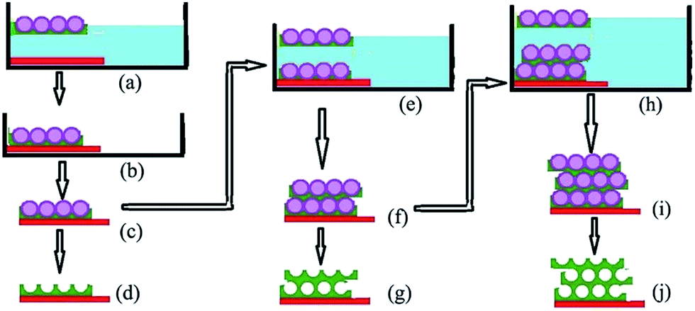 | ||
| Fig. 1 Schematics of the assembly route for the fabrication of 3D WO3 inverse opal films. Synthetic process for monolayer WO3 IO (a–d); bilayer WO3 IO (c, e, f, g); and trilayer (f, h, i, j). | ||
A WO3 aqueous-ethanol sol is then injected underneath the 2D PS spheres opal monolayer. Aided by the spreading action of ethanol, the dominant capillary forces from the interstitial space between the PS spheres attract the WO3 sol which infiltrates the interstitial space. In the process, the space between the spheres is slightly enlarged but the relative positions of the spheres are hardly changed, thus preserving the opal structure. With this procedure, the PS spheres, being in an expandable liquid/air interface, have the freedom to accommodate guest materials. A PS/WO3 opal composite monolayer structure floating over water is thus formed (Fig. 1(a)). Then, an ITO coated glass substrate is introduced underneath the floating PS/WO3 composite monolayer (Fig. 1(a)).
Next, the water contained in the system is slowly sucked out in order to have the opal composite monolayer deposit onto the ITO substrate (Fig. 1(b)). After drying, a PS/WO3 opal composite monolayer on ITO substrate is obtained (Fig. 1(c)). The thus obtained PS/WO3 opal composite monolayer on ITO substrate was then used as building block on which a second floating PS/WO3 opal composite monolayer was deposited (steps (e) to (f) of Fig. 1). Thereafter, the PS/WO3 opal composite bilayer was used as building block for the fabrication of a trilayer PS/WO3 opal composite film (steps (h) and (i) of Fig. 1). There are several advantages for this technique. First, this process takes only half an hour which is much faster than the conventional methods. Second, large-area PS/WO3 opal composite films can be obtained without any special apparatus, and only a small amount of inorganic precursor is required for each experience. Finally, the PS/WO3 opal composite films can be transferred to any kind of substrates regardless of surface wettability and smoothness.
WO3 IO monolayer (Fig. 1(d)), bilayer (Fig. 1(g)), or trilayer (Fig. 1(j)) films were produced by applying a DHF treatment after step (c), step (f) or step (i) of Fig. 1, respectively, as described in the experimental section.
Supported by the PS spheres during the formation of the multilayer PS/WO3 opal composite, the WO3 skeleton of the ordered array is retained after the removal of the PS template. As a result, all of the films show honeycomb structure with circular upper-end openings as can be seen from the SEM micrographs in Fig. 2(a)–(c) of three WO3 IO films on ITO substrates, templated from 530 nm PS spheres, consisting of monolayer (1L), bilayer (2L), and trilayer (3L), respectively. However, a change in the WO3 IO films can be seen as the number of layer is increased. Cow-nose-like porous array and trinacria form-like porous array were clearly observed in 2L and 3L IO films, respectively. The inner pores from the second layer in 3L are also apparent, which demonstrates that the porous network is interconnected throughout all three layers, allowing a good diffusion of guest materials. This is a major advantage for many potential applications since the accessibility and diffusion of chemical species within the structure is enhanced. From Fig. 2(a)–(c), it is also seen that the top openings of the three samples have nearly the same diameter (460 nm), smaller than that of the PS spheres template (530 nm), which indicates a corresponding lateral shrinkage of around 13% for all three samples, which is a little higher than earlier reports for multilayer IOs.10,24
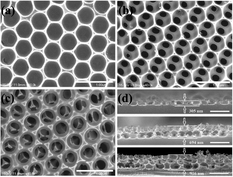 | ||
| Fig. 2 Typical SEM images of WO3 IO (a) monolayer (1L), (b) bilayer (2L), and (c) trilayer (3L) on ITO substrates after treatment in THF for 2 h followed by a heating at 150 °C for 30 min; (d) corresponding cross-section observations for monolayer (top), bilayer (middle), and trilayer (bottom). Scale bars: 1 μm. | ||
Fig. 2(d) shows cross-sectional SEM images of the 1L (top), 2L (middle), and 3L (bottom) WO3 IO films on ITO substrates. The long-range horizontal ordering and virtual absence of defects in each layer is apparent. No collapse of the WO3 walls was found for the bottom layers, this is due to the reduction of the number of steps involved in the fabrication of IO films and the use of room temperature during the fabrication process and removal of the PS spheres by chemical means instead of calcination. The absence of collapse among the different layers demonstrates the superiority of using a PS/WO3 opal composite as a substrate rather than a WO3 IO film to build the subsequent layers. As a result, the thickness of the WO3 IO increased from 305, to 694, to 916 nm for films 1L, 2L, and 3L, respectively. Considering half height infiltration for the top layer, such thickness is nearly proportional to the number of layers. Hence, the thickness of the films fabricated by this method can be precisely controlled, adding layers by simply repeating the ‘Dynamic-hard-template’ infiltration strategy.
Fig. 3 shows large area SEM images of the obtained monolayer (a), bilayer (b), and trilayer (c) WO3 IO films. These low magnification images reveal crack-free monolayer films (Fig. 3(a)) and only microcracks, of the order of the PS spheres diameter or less, are seen in the bilayer (Fig. 3(b)) and trilayer (Fig. 3(c)) WO3 IOs.
 | ||
| Fig. 3 Typical SEM image of monolayer (a); bilayer (b) and trilayer (c) WO3 IOs in low magnification (scale bar: 10 μm). | ||
Raman spectra of the WO3 IO films with various number of layers are displayed in Fig. 4. All the samples are amorphous tungsten oxide with the W![[double bond, length as m-dash]](https://www.rsc.org/images/entities/char_e001.gif) O stretching mode observed at about 965 cm−1 and a broad band present between 600 and 875 cm−1. Incidentally, amorphous and monoclinic WO3 are the most common phases synthesized and studied as working EC cathodes in EC devices.5
O stretching mode observed at about 965 cm−1 and a broad band present between 600 and 875 cm−1. Incidentally, amorphous and monoclinic WO3 are the most common phases synthesized and studied as working EC cathodes in EC devices.5
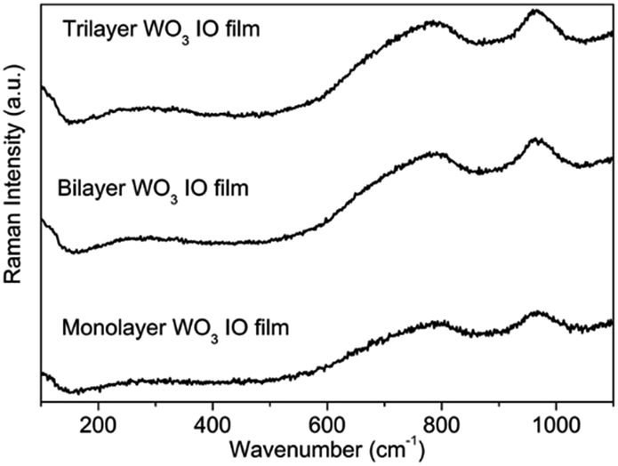 | ||
| Fig. 4 Raman spectra of WO3 IO films with various number of layers. | ||
The herein described route for the fabrication of multi-layer WO3 IO films also adds versatility to the fabrication of hierarchical IO films as illustrated in Fig. 5, where it was used for the synthesis of a hierarchical WO3 IO bilayer structure using 750 nm colloidal PS spheres for the bottom layer and 500 nm spheres for the top layer. Therefore, multilayer IO structures of different inorganic matrices with varying pore sizes could also be fabricated via repeated use of the herein described procedure. The resulting structures could have important applications in optical, photonic devices, hierarchical catalysis, etc.
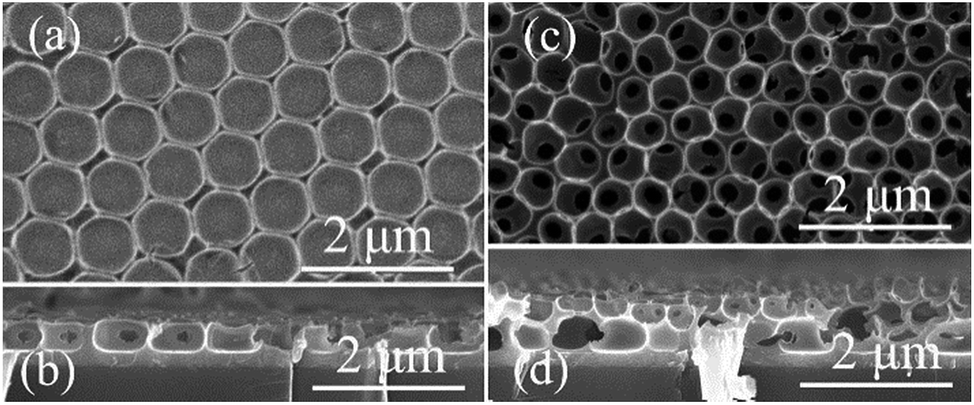 | ||
| Fig. 5 SEM images of hierarchically porous WO3 IO bilayer films synthesized from two different size PS spheres. Bottom IO layer templated from 750 nm (a) and top IO layer from 500 nm PS spheres (c) with corresponding cross-section image of bottom layer (b) and bilayer (d). | ||
Fig. 6 shows the UV-vis-NIR transmittance spectra of PS opal (monolayer) and PS/WO3 opal composite (Fig. 6(a)), and WO3 IO films (Fig. 6(b)) along with their corresponding optical reflection images (see insets). All samples show mainly blue color with different intensity levels revealing the corresponding photonic band gaps. In contrast to the PS opal monolayer, some blue shift appeared for the absorption of light from the three PS/WO3 opal composite films (around 550 nm for the PS/WO3 opal composite films as compared to 570 nm for the PS opal monolayer).
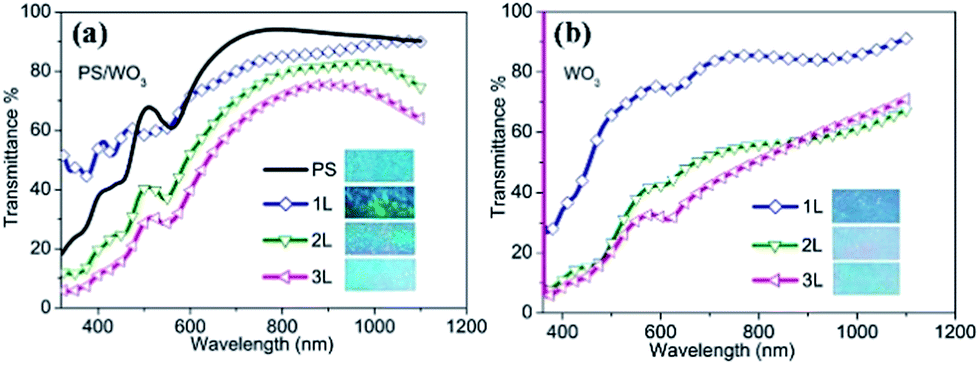 | ||
| Fig. 6 (a) UV-vis-NIR transmittance spectra of PS opal monolayer film (solid line), PS/WO3 opal composite monolayer (diamond) 1L, bilayer (up-side triangle) 2L and trilayer (oblique triangle) 3L. (b) WO3 IOs films, 1L (diamond), 2L (up-side triangle) and 3L (oblique triangle). Insets show the corresponding optical reflection images from PS opal monolayer, PS/WO3 opal composites and WO3 IO films on ITO substrates taken on black background. | ||
Apart from the absorption at 550 nm, there are several minor absorptions from 400 to 500 nm, contributing to the blue color at various levels. After the removal of the PS templates, a clear attenuation band in the transmittance spectra shown in Fig. 6(b) can be observed. However, the absorption shows a red-shift from 550 nm for the PS/WO3 opal composite films (Fig. 6(a)) to around 620 nm for the WO3 IO films (Fig. 6(b)). Coupled with some minor absorption around 450 nm, a pale pink doped main blue is observed in all three samples of WO3 IOs. The transmittance of the IO films was 81.5, 65.6 and 53.3% at 700 nm wavelength for 1L, 2L and 3L, respectively, and 84.7, 80.6, and 67.0% at 1100 nm, for 1L, 2L and 3L, respectively.
The electrochromic behaviour of ITO-based WO3 IO films with different number of layers was evaluated, and their optical transmittance spectra in colored and bleached states for applied potentials of ±2.0 V are shown in Fig. 6(a) after 1 cycle, and in Fig. 6(b) after 10 cycles. The actual photographs of the WO3 IO films in colored states are also presented as insets in Fig. 7. For cycle 1, in the bleached state, the transmittance of the films at a wavelength of 700 nm (Vis) was 80.8% for 1L, 74% for 2L, and 51.3% for 3L, whereas, at a wavelength of 1100 nm (NIR), the transmittance was 83.6% for 1L, 84% for 2L, and 69% for 3L. As shown in Table 1, when the coloration potential of 2.0 V is applied, the transmittance of the films at a wavelength of 700 nm is reduced and the films exhibited an optical contrast of 21.4, 32.1, and 31.7% for 1L, 2L and 3L, respectively. However, at a wavelength of 1100 nm the optical contrast for 1L remains practically unchanged (22.5%) as compared to that observed at 700 nm, for which wavelength it increased to 38.4 and 46% for 2L and 3L, respectively. This indicates a difference in optical absorption between the visible and IR regions as the number of layer is increased. It was also observed that the coloration became deeper for 2L and 3L samples after 10 cycles (Fig. 7(b)), which indicates that the coloration reactions keeps on going due to the diffusion effect. The optical contrast for 2L sample at 700 nm and 1100 nm reached 45.7% and 57.6%, respectively. For 3L though, a decrease in the optical contrast was observed at cycle 10 for both the visible and infrared regions as seen in Table 1.
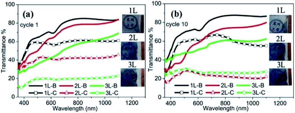 | ||
| Fig. 7 Transmittance spectra of WO3 IO films with different number of layers recorded at colored (C) (2.0 V, 10 s) and bleached (B) (−2.0 V, 10 s) states. The insets show typical photographs of the WO3 IO films at the colored state, illustrating a distinct optical contrast. 1L, 2L and 3L refer to monolayer, bilayer and trilayer WO3 IO films, respectively. | ||
| Sample | At 700 nm | At 1100 nm | ||
|---|---|---|---|---|
| ΔTa (%) | ΔODb | ΔTa (%) | ΔODb | |
| a ΔT (%) at 700 nm (or 1100 nm) = Tbleached (%) − Tcolored (%).b ΔOD at 700 nm (or 1100 nm) = log(Tbleached (%)/Tcolored (%)). | ||||
| Cycle 1 | ||||
| 1L | 21.4 | 0.134 | 22.5 | 0.136 |
| 2L | 32.1 | 0.247 | 38.4 | 0.265 |
| 3L | 31.7 | 0.418 | 46 | 0.477 |
|
||||
| Cycle 10 | ||||
| 1L | 16.9 | 0.0987 | 31.6 | 0.195 |
| 2L | 45.7 | 0.470 | 57.6 | 0.554 |
| 3L | 31.3 | 0.339 | 34.8 | 0.353 |
Fig. 8 displays cyclic voltammograms (CV) recorded for the WO3 IO films at a constant scan rate of 2 mV s−1. The films exhibit a good electrochemical reversibility and cycling stability, which is reflected by the absence of shrinking in the peak current densities during all the cycles. The electrochromic performance of the WO3 IO films was estimated by their coloration efficiency (CE) at a particular wavelength, defined by CE(λ) = ΔOD/q, where ΔOD is the optical density change occurring in the film with lithium insertion and q is the charge inserted in the film. The charge is calculated from the CV of respective films.
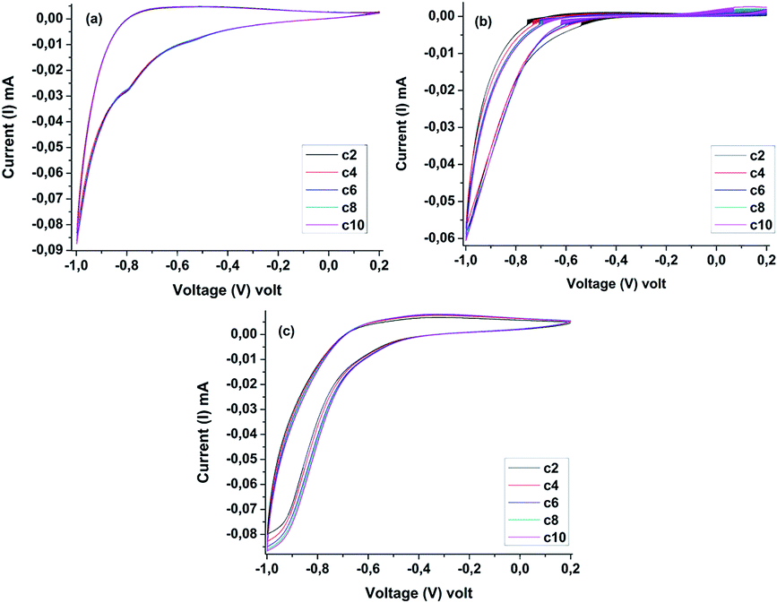 | ||
| Fig. 8 Cyclic voltammograms (CV) of WO3 IO films: monolayer (a), bilayer (b), and trilayer (c) obtained with 0.5 M LiClO4 in dimethyl sulfoxide (DMSO) for 10 cycles at a scan rate of 2 mV s−1. | ||
The calculated CE for the first and tenth cycles at 700 and 1100 nm wavelengths of the WO3 IO films are shown in Table 2. As seen in Table 2, CE is noticed to increase as the number of layer is increased, and tends to increase during cycling. Concurrently, the optical images of the WO3 IO films (inset of Fig. 7) show an increased coloration as the number of layers is increased. These results thus render the WO3 IO films suitable for practical electrochromic windows.
| Sample | CE 1st cycle (cm2 C−1) | CE 10th cycle (cm2 C−1) | ||
|---|---|---|---|---|
| At 700 nm | At 1100 nm | At 700 nm | At 1100 nm | |
| 1L | 8 | 13 | 10 | 15 |
| 2L | 16 | 25 | 16 | 25 |
| 3L | 19 | 31 | 24 | 40 |
Sample 3L exhibits the highest CE of 40 cm2 C−1 at a wavelength of 1100 nm. The increase in CE with increasing number of layers is related to the photonic effect as well as the increase in electrochromic material.
To the best of our knowledge, there are very few reports of WO3 inverse opal film used as active electrode in EC devices. Nevertheless, the CE of 40 cm2 C−1 obtained for the 3L sample measured at 1100 nm compares favourably with a 3D ordered macroporous IO WO3 film prepared by the conventional vertical convective self-assembly method reported by Badilescu et al., in which CE was found to be 35 cm2 C−1.30 Alsawafta et al. reported a higher CE of 70 cm2 C−1 for a macroporous WO3 IO film doped with Au nanoparticles. However, they attributed this high result to the presence of the Au nanoparticles in the WO3 IO film.31 Wei Cheng et al. reported CE values of around 21 cm2 C−1 for mesoporous WO3 prepared from WCl6 by a sol–gel method.32 Also, the present CE result of 40 cm2 C−1 exceeds the 25 cm2 C−1 of a pulsed laser deposited WO3 film,33 while for sputtered films CE is 34 cm2 C−1.34 For sol–gel films deposited by dip-coating and heated at 150 °C, CE is reported to be 30 cm2 C−1.35 Spin-coated sol–gel crystalline WO3 films have CE of only about 20–25 cm2 C−1.36 Thus, the CE results in this work for the 3L sample is higher than most of the values reported in the literature for pure WO3 IO films.
Conclusions
In summary, three-dimensional highly ordered inverse opal films were designed and successfully fabricated by using PS/WO3 opal composite monolayers obtained from a “Dynamic-hard-template” infiltration strategy as building block. We have demonstrated that WO3 monolayer, bilayer and trilayer IO films, with the same pore size in each layer, can be obtained via repeated operations of the “Dynamic-hard-template” infiltration strategy. Furthermore, we have demonstrated the flexibility of the “Dynamic-hard-template” infiltration approach for the fabrication of multilayered hierarchical IO films by allowing a variation in macropore sizes and/or material from layer to layer. Due to the highly ordered macroporous texture, allowing an improved access of the electrolyte, the WO3 IO films exhibit a good electrochemical reversibility, cycling stability, and increased coloration efficiency (CE) as the number of layers is increased. Thus, those WO3 IO films could find promising applications in electrochromic windows, chemical sensors, and so on.Conflicts of interest
There are no conflicts to declare.Acknowledgements
The financial support of National Natural Science Foundation of China (grant #21301123), China Scholarship council, Priority Academic Program Development of Jiangsu Higher Education Institutions, the National Science and Engineering Research Council (NSERC) of Canada (grant #2017-05094), the John R. Evans Leaders Fund (Canada Foundation for Innovation) (grant #27741), and of the Research Assistantships Initiative of New Brunswick Innovation Fund (NBIF) is gratefully acknowledged. We also greatly thank the help in micro-Raman characteristic from Tianjin Gangdong SCI&Tech. Development Co. LTD.References
- C. G. Granqvist, Out of niche, Nat. Mater., 2006, 5, 89–90 CrossRef CAS PubMed.
- S. K. Deb, Opportunities and challenges in science and technology of WO3 for electrochromic and related applications, Sol. Energy Mater. Sol. Cells, 2008, 92, 245–258 CrossRef CAS.
- S. Balaji, A.-S. Albert, Y. Djaoued and B. Brüning, Micro-Raman Spectroscopic characterization of tunable electrochromic device for application in smart windows, J. Raman Spectrosc., 2009, 40, 92–100 CrossRef CAS.
- M. F. Daniel, B. Desbat, J. C. Lassegues, B. Gerand and M. Figlarz, Infrared and Raman study of WO3 tungsten trioxides and WO3, xH2O tungsten trioxide hydrates”, J. Solid State Chem., 1987, 67, 235–247 CrossRef CAS.
- E. Cazzanelli, C. Vinegoni, G. Mariotto, A. Kuzmin and J. Purans, Raman study of the phase transitions sequence in pure WO3 at high temperature and in HxWO3 with variable hydrogen content, Solid State Ionics, 1999, 123, 67–74 CrossRef CAS.
- W. J. Hyun, H. K. Lee, S. S. Oh, O. Hess, C.-G. Choi, -H. ImS and O. O. Park, Two-Dimensional TiO2 Inverse Opal with a Closed Top Surface Structure for Enhanced Light Extraction from Polymer Light-Emitting Diodes, Adv. Mater., 2011, 23, 1846–1850 CrossRef CAS PubMed.
- S. Balaji, Y. Djaoued, A.-S. Albert, R. Z. Ferguson and R. Brüning, Hexagonal tungsten oxide based electrochromic devices: spectroscopic evidence for the Li ion occupancy of four coordinated square windows, Chem. Mater., 2009, 21, 1381–1389 CrossRef CAS.
- Y. Djaoued, S. Priya and S. Balaji, Low temperature synthesis of nanocrystalline WO3 films by sol–gel process, J. Non-Cryst. Solids, 2008, 354, 673–679 CrossRef CAS.
- E. Stathatos, P. Lianos, U. L. Štangar and B. Orel, A high-performance solid-state dye-sensitized photoelectrochemical cell employing a nanocomposite gel electrolyte made by the sol–gel route, Adv. Mater., 2002, 14, 354–357 CrossRef CAS.
- K. Eun Sik, L. Wonmok, P. Nam-Gyu, K. Junkyung and L. Hyunjung, Compact inverse-opal electrode using non-aggregated TiO2 nanoparticles for dye-sensitized solar cells, Adv. Funct. Mater., 2009, 19(7), 1093–1099 CrossRef.
- K. Xie, M. Guo and H. T. Huang, Photonic crystals for sensitized solar cells: fabrication, properties, and applications, J. Mater. Chem. C, 2015, 3, 10665–10686 RSC.
- E. Armstrong and C. O'Dwyer, Artificial opal photonic crystals and inverse opal structures – fundamentals and applications from optics to energy storage, J. Mater. Chem. C, 2015, 3, 6109–6143 RSC.
- I. B. Burgess, L. Mishchenko, B. D. Hatton, M. Kolle, M. Lončar and J. Aizenberg, Encoding Complex Wettability Patterns in Chemically Functionalized 3D Photonic Crystals, J. Am. Chem. Soc., 2011, 133(32), 12430–12432 CrossRef CAS PubMed.
- S.-W. Choi, J.-W. Xie and Y.-N. Xia, Chitosan-based inverse opals: three-dimensional scaffolds with uniform pore structures for cell culture, Adv. Mater., 2009, 21, 2997–3001 CrossRef CAS PubMed.
- I. Jennifer, L. Chen, G. V. Freymann, V. Kitaev and G. A. Ozin, Effect of Disorder on the Optically Amplified Photocatalytic Efficiency of Titania Inverse Opals, J. Am. Chem. Soc., 2007, 129(5), 1196–1202 CrossRef PubMed.
- K. R. Phillips, N. Vogel, Y.-H. Hu, M. Kolle, C. C. Perry and J. Aizenberg, Tunable anisotropy in inverse opals and emerging optical properties, Chem. Mater., 2014, 26, 1422–1628 CrossRef.
- B. Hatton, L. Mishchenko, S. Davis, H. S. Kenneth and J. Aizenberg, Assembly of large-area, highly ordered, creak-free inverse opal films, Proc. Natl. Acad. Sci. U. S. A., 2010, 107(23), 10354–10359 CrossRef CAS PubMed.
- Y. H. Kim, H. Kang, S. Park, A. R. Park, Y. M. Lee, D. K. Rhee, S. Han, H. Chang, Y. Du R.- and P. J. Yoo, Multiscale porous interconnected nanocolander network with tunable transport properties, Adv. Mater., 2014, 26, 7998–8003 CrossRef CAS PubMed.
- B. H. Juárez, P. D. García, D. Golmayo, A. Blanco and C. López, ZnO Inverse Opals by Chemical Vapor Deposition, Adv. Mater., 2005, 17, 2761–2765 CrossRef.
- X. S. Zhao, F.-B. Su, Q.-F. Yan, W.-P. Guo, X.-Y. Bao, L. Lv and Z.-C. Zhou, Templating methods for preparation of porous structures, J. Mater. Chem., 2006, 16, 637–648 RSC.
- B. T. Holland, C. F. Blanford, T. Do and A. Stein, Synthesis of Highly Ordered, Three-Dimensional, Macroporous Structures of Amorphous or Crystalline Inorganic Oxides, Phosphates, and Hybrid Composites, Chem. Mater., 1999, 11, 795–805 CrossRef CAS.
- A. Stein, F. Li and N. R. Denny, Morphological Control in Cplloidal Crystal Templating of Inverse Opals, Hierarchical Structures, and Shaped Particles, Chem. Mater., 2008, 20, 649–666 CrossRef CAS.
- O. D. Velev and A. M. Lenhoff, Colloidal crystals as templates for porous materials, Curr. Opin. Colloid Interface Sci., 2000, 5, 56–63 CrossRef CAS.
- Y.-G. Seo, K. Woo, J. Kim, H. Lee and W. Lee, Rapid Fabrication of an Inverse Opal TiO2 Photoelectrode for DSSC Using a Binary Mixture of TiO2 Nanoparticles and Polymer Microspheres, Adv. Funct. Mater., 2011, 21, 3094–3103 CrossRef CAS.
- H. Miguez, N. Tétreault, B. Hatton, S. M. Yang, D. Perovic and G. a. Ozin, Mechanical Stability Enhancement by Pore Size and Connectivity Control in Colloidal Crystals by Layer-by-layer Growth of Oxide, Chem. Commun., 2002, 2736–2737 RSC.
- Y. Kimura, S. Kaneda, T. Fujii and S. Murata, Layer-by-Layer Assembly of Photonic Crystal Using DNA, Electron Comm Jpn, 2013, 96(5), 286–291 Search PubMed.
- H.-W. Zhang, G.-T. Duan, G.-Q. Liu, Y. Li, X.-X. Xu, Z.-F. Dai, J.-J. Wang and W.-P. Cai, Layer-controlled synthesis of WO3 ordered nanoporous films for optimum electrochromic application, Nanoscale, 2013, 5, 2460–2468 RSC.
- R. Gao, L.-F. Hu, M. Chen and L.-M. Wu, Controllable Fabrication and Photoelectrochemical Property of Multilayer Tantalum Nitride Hollow Sphere-Nanofilms, Small, 2014, 10(15), 3038–3044 CrossRef CAS PubMed.
- H. Li, G. Vienneau, M. Jones, B. Subramanian, J. Robichaud and Y. Djaoued, Crack-Free 2D-Inverse Opal Anatase TiO2 Films on Rigid and Flexible Transparent Conducting Substrates : Low Temperature Large Area Fabrication and Electrochromic Property, J. Mater. Chem. C, 2014, 2, 7804–7810 RSC.
- S. Badilescu and P. V. Ashrit, Study of sol–gel prepared nanostructured WO3 thin films and composites for electrochromic applications, Solid State Ionics, 2003, 158, 187–197 CrossRef CAS.
- M. Alsawafta, Y. M. Golestani, T. Phonemac, S. Badilescu, V. Stancovski and T. Vo-Van, Electrochromic Properties of Sol–Gel synthesized Macroporous Tungsten Oxide Films doped with gold Nanoparticles, J. Electrochem. Soc., 2014, 161, H276–H283 CrossRef CAS.
- W. Cheng, E. Baudrin, B. Dunn and J. I. Zinc, Synthesis and electrochromic properties of mesoporous tungsten oxide, J. Mater. Chem., 2001, 11, 92–97 RSC.
- A. F. Rougier, F. A. Portemer, A. Quédé and M. El Marssi, Characterization of pulsed laser deposited WO3 thin films for electrochromic devices, Appl. Surf. Sci., 1999, 153, 1–9 CrossRef CAS.
- S. Taunier, C. Guery and J.-M. Tarascon, Design and characterization of a three-electrode electrochromic device, based on the system WO3/IrO2, Electrochim. Acta, 1999, 44, 3219–3225 CrossRef CAS.
- C. G. Granqvist, Handbook of Inorganic Electrochromic Materials, 2002, Elsevier, Amsterdam, p. 263 Search PubMed.
- N. Ozer, M. Demirbas and S. Ozyurt, In situ spectroscopic studies of electrochromic tungsten oxide films, Proc. SPIE, 2001, 4458, 169–189 CrossRef CAS.
| This journal is © The Royal Society of Chemistry 2017 |