
 Open Access Article
 This Open Access Article is licensed under a
 Creative Commons Attribution 3.0 Unported Licence
Molybdenum trioxide thin film recombination barrier layers for dye sensitized solar cells
Aditya Ashok,
S. N. Vijayaraghavan ,
Shantikumar V. Nair* and
Mariyappan Shanmugam*
,
Shantikumar V. Nair* and
Mariyappan Shanmugam*
Center for Nanosciences and Molecular Medicine, Amrita University, Kochi-682041, Kerala, India. E-mail: nairshanti@gmail.com; mshanmugham@aims.amrita.edu
First published on 16th October 2017
Abstract
A physical vapor deposition based molybdenum trioxide (MoO3) thin film is demonstrated as an efficient reverse-electron recombination barrier layer (RBL) at the fluorine doped tin oxide (FTO)/titanium dioxide (TiO2) interface in dye sensitized solar cells (DSSCs). Thin films of MoO3 show an average optical transmittance of ∼77% in a spectral range of 350–800 nm with bandgap value of ∼3.1 eV. For an optimum thickness of MoO3, deposited for 5 minutes, the resulting DSSCs showed 15% enhancement in efficiency (η) compared to the reference DSSC which did not use MoO3 RBL; this suggests that MoO3 is effectively suppressing interfacial recombination at the FTO/TiO2 interface. Further, increasing the thickness of MoO3 RBL at the FTO/TiO2 interface (20 minutes deposition) is observed to impede charge transport, as noticed with 55% reduction in η compared to the reference DSSC. Thin film MoO3 RBL with an optimum thickness value at the FTO/TiO2 interface efficiently blocks the leaky transport pathways in the mesoporous TiO2 nanoparticle layer and facilitates efficient charge transport as confirmed by electrochemical impedance spectroscopy.
1 Introduction
Hybrid photovoltaic technology offers unique opportunities to employ both organic and inorganic photo-active functional materials in solar cells.1–3 Nanocrystalline titanium dioxide (TiO2) based dye sensitized solar cells (DSSCs), a technologically important hybrid photovoltaic category, have shown potential merits in terms of performance and cost.4–7 While the DSSC is considered as a potential competitor for inorganic solar cell technologies, a few major factors have been realized as major technical hurdles for further progress in terms of performance and stability.8–12 Various issues associated with dyes including narrow band photo-absorption, inefficient electron injection into TiO2, defects present in the nanocrystalline electron transport layer, volatile/corrosive liquid electrolytes are significant factors that have been under research for more than two decades.13 Different nanostructures of TiO2, including nanotubes, nanowires, nanofibers and nanoparticles, are widely employed as electron transport layer due to their own optical and electrical advantages.14–17 Large surface area of the electron transport layers are highly preferred in excitonic solar cells to adsorb more photo-sensitizing materials such as organic dyes and quantum dots.18,19 TiO2 film thickness, sizes of particles and pores present in the film are a few important material properties that determine the performance of DSSCs.20–23 The surface area in the nanocrystalline material can be tuned by varying the particle size. In general, unsaturated atomic bonds (dangling bands) on the surface of TiO2 result as surface states which are considered to be defect states which actively play a detrimental role on charge transport.24,25 While surface area of TiO2 is increased, the density of surface states that are present on the surface also increases. This situation offers certain advantages to DSSCs optically and disadvantages electrically. The hole conductor, often liquid electrolyte, diffuses into the bulk of dye coated TiO2 to form the junction through which the dye molecules are regenerated. Thus, the interfaces between TiO2/dye/electrolyte are important at which significant photovoltaic processes occur. While the TiO2 allows the electrolyte to form the junction throughout the bulk, it might make an electrical contact with transparent electrode which is essentially an unwanted short circuit and the resulting solar cell will not be functional. To avoid such unwanted situation, a thinner TiO2 layer of smaller particle size was introduced into the transparent electrode and TiO2 interface, called compact layer.26 The ions in the liquid electrolyte can diffuse into the mesoporous TiO2 but will be blocked by compact TiO2 due to the smaller size nanoparticles. Other than TiO2 nanoparticles, various other materials, such as ZnO and HfO2, have been explored for compact layer applications and observed to enhance the performances significantly.27,28 All these studies show that compact layers in DSSCs should be highly dense, pin hole-free, and less defective to block the reverse electron transport from the transparent electrode to the electrolyte in which holes will be available for recombination. Further, effect of metal doping in compact layers, for example Li and Nb, and surface treatment by TiCl4 were examined to control the recombination loss in DSSCs.29–31 All these studies show a major requirement to control the photo-generated electron recombination at the interface of transparent electrode and mesoporous TiO2. Suppressing such interfacial recombination in DSSCs, in general, is one of the ways to improve the performance of resulting DSSCs.Molybdenum trioxide (MoO3), an orthorhombic crystal structured material, exhibits an optical bandgap of ∼3.1 eV with a work function 5.3 eV. Efficient hole injection characteristics of MoO3 have been studied in transparent conductor oxide (TCO) and organic hole transporting materials.32–34 Physical/chemical vapor deposited MoO3 thin films have shown promising applications in gas sensing and electro-chromic devices.35,36 F. Cheng et al. has recently reported the organic solar cells employing MoO3 based hole transport layer.37 Various material processing methods including physical/chemical vapor deposition, flash evaporation, ion beam and wet-chemical based techniques are commonly used to deposit MoO3.38–40
In this work, capability of thin film MoO3, deposited by reactive DC sputtering, as a reverse electron RBL is examined in DSSCs. Further, effect of deposition time (thickness) on the performance of DSSCs was studied and it was observed that there is an optimum MoO3 thickness to suppress the interfacial recombination by facilitating the electron transport and blocking the holes at FTO/TiO2 interface. The presented results also clarify the increased thickness of MoO3 impede the charge transport by establishing an energy barrier at FTO/TiO2 interface. Thus, MoO3 thin film can be considered as a dense and pin-hole free RBL for DSSCs.
2 Experimental section
(i) Fabrication of reference DSSCs
To explore and prove the concept of MoO3 thin film based RBLs, two kinds of DSSCs were fabricated (1) DSSCs employing mesoporous TiO2 as an electron transport layer, coated directly on FTO electrode. This DSSC was considered as a reference cell to evaluate the effect of MoO3 RBLs. (2) DSSCs with MoO3 thin films as RBLs coated on FTO. To fabricate the reference DSSC, ∼10 μm thick colloidal TiO2 nanoparticle layer was coated onto FTO coated glass substrate by doctor blade method followed by annealing at 450 °C for 1 hour. The TiO2 coated on FTO was sensitized by Ruthenium based N719 dye for 12 hours. The dye solution used in this study was prepared by dissolving 0.5 mM of N719 in 1![[thin space (1/6-em)]](https://www.rsc.org/images/entities/char_2009.gif) :1 mixture of acetonitrile and tertbutyl alcohol solution. Commercially available Iodolyte AN-50 was used as a hole transporting layer. A 50 nm Pt thin film was used as a counter electrode. Dye coated TiO2 photo-anode and the Pt coated counter electrode was coupled using a parafilm spacer and the electrolyte was injected between the electrodes through a channel made on a parafilm spacer and sealed before measurements. No TiCl4 treatment and TiO2 blocking layer were used in this work to examine the effect only due to MoO3 in DSSC performance without considering any other surface modifications that are usually followed in DSSC fabrication procedure.
:1 mixture of acetonitrile and tertbutyl alcohol solution. Commercially available Iodolyte AN-50 was used as a hole transporting layer. A 50 nm Pt thin film was used as a counter electrode. Dye coated TiO2 photo-anode and the Pt coated counter electrode was coupled using a parafilm spacer and the electrolyte was injected between the electrodes through a channel made on a parafilm spacer and sealed before measurements. No TiCl4 treatment and TiO2 blocking layer were used in this work to examine the effect only due to MoO3 in DSSC performance without considering any other surface modifications that are usually followed in DSSC fabrication procedure.
(ii) Fabrication of MoO3 coated DSSCs
To demonstrate MoO3 as a potential candidate for RBL application in DSSCs, thin films of MoO3 were deposited onto FTO by reactive DC sputtering using oxygen as a bombarding gas and molybdenum as a metal target. Oxygen flow rate was kept at 30 sccm and all MoO3 films were deposited at 200 °C. The films were deposited for 5, 10, 15 and 20 minutes to study the effect of thickness of MoO3 on the performance of DSSCs. The MoO3 deposited FTO electrodes were used to coat mesoporous TiO2 electron transport layer. The remaining fabrication procedure is the same as explained in case of reference DSSC fabrication.(iii) Fabrication of DSSCs with TiCl4 coated FTO
Titanium tetrachloride (TiCl4) stock solution was freshly prepared as reported by S. Ito et al.41 FTO coated glass substrates were dipped in TiCl4 for 30 minutes at 70 °C and annealed at 450 °C for 30 minutes. In order to fabricate DSSCs using TiCl4 coated FTO, the mesoporous TiO2 was coated onto FTO/TiCl4 electrode and annealed at 450 °C for 1 hour. The remaining fabrication steps are the same as explained in reference DSSC fabrication.(iv) Materials and DSSC characterizations
Morphology of the TiO2 and MoO2 thin film samples were analyzed in a scanning electron microscope (SEM) using JSM-6490-LA from JEOL. X-ray photoelectron spectroscopy (XPS) was used to confirm the thin films of MoO3 using Kratos Analytical unit. Optical characteristics of the MoO3 films, FTO and N719 were studied by Perkin Elmer Lambda-750 UV-Visible spectrometer. The current density–voltage (J–V) measurements of the DSSCs were performed under AM1.5 illumination level using Newport Oriel Class A solar simulator and a digital source meter (Keithley 2400). Electrochemical Impedance Spectroscopic (EIS) studies were performed in the reference and the DSSCs employing MoO3 RBLs under dark condition using Autolab electrochemical work station.3 Results and discussion
Fig. 1 shows SEM images illustrating the surface morphologies of (a) TiO2 nanoparticles coated onto FTO electrode and (b–e) reactive DC sputtered MoO3 RBLs on the FTO substrates. The TiO2 nanoparticle layer is observed to be highly porous and having ∼20 nm nanoparticles distributed randomly. The TiO2 nanoparticle network is well connected through which photo-generated electrons diffuse to reach the FTO electrode. Physical connectivity among the nanoparticles, particle distribution and electrical conductivity play a significant role on charge transport in the bulk TiO2 nanoparticle network. However, it is obvious that the electrolyte ions can diffuse through such porous layer and this situation is expected to result in unwanted electrical short with FTO electrode. While the porosity of TiO2 nanoparticle layer assists in dye loading, electrolyte diffusion towards FTO electrode is an unwanted situation in DSSCs. Fig. 1(b–e) show surface morphologies of MoO3 at different magnifications. These morphologies assert there is no porosity in the bulk as can be observed in the TiO2 nanoparticle film shown in Fig. 1(a). This is a major requirement for a material to performance as an efficient RBL in DSSCs to suppress the electrolyte diffusion towards the FTO. A pinhole-free thin film with no porosity is expected to block the electrolyte ions and avoid direct electrical contact between the hole transport layer and electron-collecting electrode. The MoO3 particles distributed in the samples were random in sizes but their packing fraction is observed to be higher than that of TiO2 nanoparticle layer, which is an essential factor to effectively block the hole transporting electrolyte from touching the FTO. Fig. 1(b, c, d and e) obtained under the magnifications of 5000×, 10000×, 20000× and 30000× respectively.
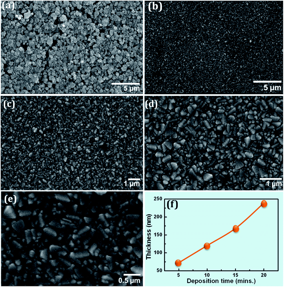 | ||
| Fig. 1 SEM images showing (a) porous TiO2 exhibiting randomly distributed TiO2 nanoparticles in a porous network, (b–e) show MoO3 RBL coated onto FTO at different magnifications show a better compactness through which diffusion of electrolyte was significantly suppressed and (f) deposition time vs. thickness of MoO3 obtained. | ||
While the lower magnification images show uniform distribution of particles, the image obtained at 30000× illustrates the surface is covered by tightly bound MoO3 particles of different size distribution. Larger size particles are observed to be on the surface while the gap between the larger particles are perfectly filled with relatively smaller size MoO3 particle distribution as can be observed in Fig. 1(e). Thus, the MoO3 film is highly dense due to the filling effect of smaller size particles among the distribution larger size particles. In general, colloidal TiO2 nanoparticles are used for compact layer applications in DSSCs. However, the colloidal layer also is expected to have porosity to certain extent due to its nature of morphology. Physical vapor deposition, in general, offers highly uniform, dense and compact thin films through which electrolyte diffusion is not expected due to the tightly arranged particle distribution as can be seen in Fig. 1(b–e). It is very obvious that presence of such highly compact metal oxide layer at the interface of FTO/TiO2 act as a barrier for any kind of liquid materials, in this case it is hole transporting electrolyte. This particular sample illustrated in Fig. 1(b–e) was deposited at 200 °C for 20 minutes. Profilometer measured thickness values of the samples deposited for 5, 10, 15 and 20 minutes were 70 nm, 120 nm, 170 nm and 240 nm respectively as shown in Fig. 1(f).
XPS studies were performed on MoO3 thin film deposited on glass substrate to confirm and examine various constituting elements, particularly molybdenum and oxygen. Fig. 2(a) shows XPS survey spectrum obtained on the MoO3 sample illustrating characteristic peaks of molybdenum, oxygen and carbon in the binding energy range of 0–700 eV. The wide scan survey spectrum showed Mo 4p at 42 eV, Mo 3d at 235 eV, C 1s at 284 eV and O 1s at 529 eV. Doublet core levels of MoO3 shown in the survey spectrum was further studied through a high resolution scan. Fig. 2(b and c) show high resolution XPS characteristic spectra of Mo 3d and O 1s peaks respectively. The spin orbit doublet of MoO3 is further deconvoluted as shown in Fig. 2(c), confirming the Mo 3d5/2 and Mo 3d3/2 observed at 232.6 eV and 235.8 eV correspond to Mo6+ in stoichiometric MoO3 film. The O 1s peak is comprised of two different contributions as shown in deconvoluted high resolution scan in Fig. 2(c). The peak fit identified 528.5 eV corresponding to Mo![[double bond, length as m-dash]](https://www.rsc.org/images/entities/char_e001.gif) O bonding between molybdenum and oxygen while 531.0 eV represents the OH group adsorbed on the surface of the MoO3 film.
O bonding between molybdenum and oxygen while 531.0 eV represents the OH group adsorbed on the surface of the MoO3 film.
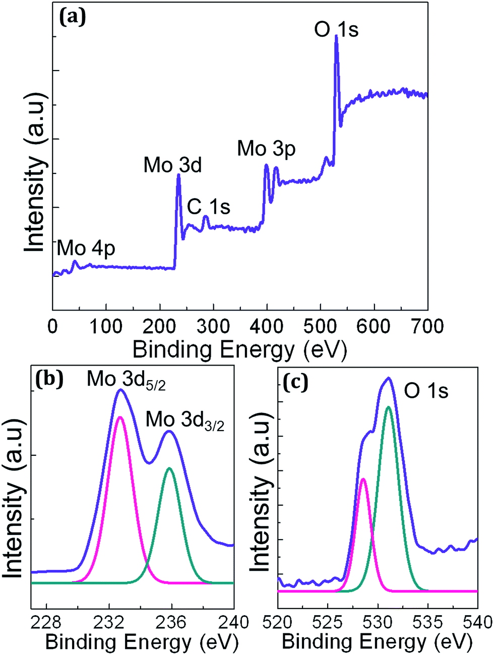 | ||
| Fig. 2 XPS spectra of PVD grown MoO3 thin film sample showing (a) wide scan survey spectrum and high resolution scans of (b) Mo 3d and (c) O 1s characteristic peaks. | ||
Fig. 3 shows UV-Visible optical spectroscopic characteristics of MoO3 samples along with the FTO used for DSSC fabrication illustrating absorbance and transmittance in a wavelength window of 350–800 nm. The MoO3 samples exhibit slightly more absorbance and less transmittance compared to the FTO and their optical absorbance and transmittance characteristics overlap on each other as shown in Fig. 2(a) due to the smaller variation in their thickness offered by the duration of deposition which are 5, 10, 15 and 20 minutes. Fig. 3(b and c) shows the magnified view of the absorbance and transmittance spectra shown in Fig. 3(a) in a spectral region of 350–700 nm showing the smaller variation clearly. The FTO, a wide bandgap metal oxide transparent conductor, exhibits no photonic absorption in the spectral window of 350–800 nm. This confirms that incoming photons don't lose their energy at the electrode while reaching the photo-active material; in this case it is N719. Further, UV-Visible optical characteristics of MoO3 films also exhibit similar features confirming that photonic loss at the RBL also will be very minimum. Thus, optical loss at FTO electrode and MoO3 RBL is considered to be insignificant. Further, absorption coefficient (α) values for all MoO3 samples were calculated from the transmittance spectra and used to calculate optical bandgap values through Tauc plot technique shown in Fig. 4(a). The characteristic spectra (αhν)1/2 vs. energy of incoming photons at (αhν)1/2 = 0 yields optical bandgap values of MoO3 samples deposited for 5, 10, 15 and 20 minutes.
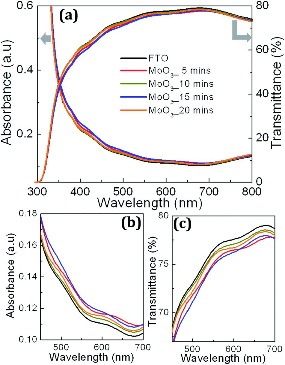 | ||
| Fig. 3 (a) Optical absorption and transmittance spectra of FTO along with MoO3 samples deposited on FTO for 5, 10, 15 and 20 minutes show overlap in the characteristics due to the slight variation (the arrows indicate the axes for the absorbance and transmittance characteristics). (b and c) Magnified absorbance and transmittance showing clear variation in a spectral window of 450–700 nm. | ||
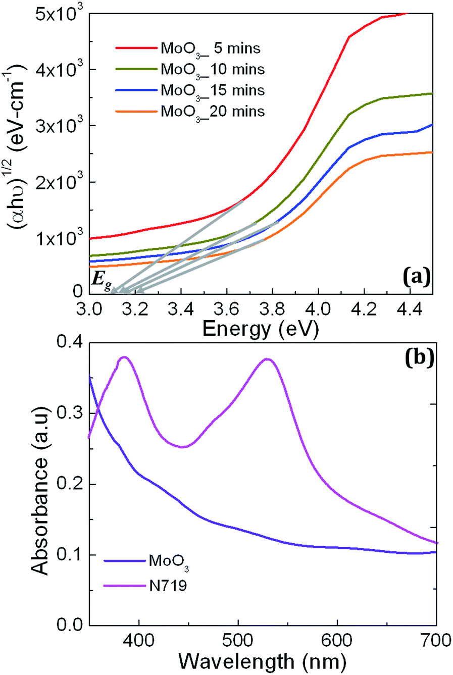 | ||
| Fig. 4 (a) Optical bandgap values of all MoO3 samples from (αhν)1/2 vs. energy of the incoming photons, (b) comparison of absorbance of MoO3 and N719 dye to confirm the optical inactiveness of MoO3 in the spectral window of 350–700 nm in which N719 is optically active in terms of photo-absorption. | ||
The extracted bandgap values for all samples were about ∼3.1 eV with ∼0.1 eV variation for the sample processed for 20 minutes. The observed insignificant variation in the bandgap value (0.1 eV), can be ignored due to the cause of longer duration of oxygen flow which alters the band structure slightly. The value of optical bandgap obtained for MoO3 samples confirm that incoming solar photons in a wavelength range of 350–800 nm do not interact with MoO3. It implies that MoO3, as a RBL in DSSCs, does not block the visible spectral photons which supposed to be absorbed by N719 used as a major photo-active dye layer on mesoporous TiO2. To illustrate the “optical compatibility” between the MoO3 and N719, absorbance characteristics of MoO3 and N719 dye are compared as shown in Fig. 4(b). The two major peaks observed at 385 nm and 525 nm in the absorbance spectrum confirm N719 while the near-flat characteristic represents MoO3 due to the optical bandgap of 3.1 eV shown in Fig. 4(a). It is obvious that MoO3 is not expected to absorb solar photons in the visible spectral window as a passive material component in DSSCs. It is expected to simply pass the visible spectral photons towards N719 at which major photonic absorption process occurs. Fig. 4(b) confirms MoO3 behaves optically inactive, in terms of absorption, in the spectral window of 350–800 nm where N719 is optically active to absorb the visible energy. The optical absorbance and transmittance characteristics with a bandgap value of 3.1 eV support MoO3 as a potential RBL at FTO/TiO2 interface to suppress the recombination loss in DSSCs. Further, the four samples considered in this work, deposited at 5, 10, 15 and 20 minutes, exhibit insignificant optical loss in the visible spectral range due to the wide bandgap which is an essential requirement for RBLs.
Fig. 5(a) shows J–V characteristics of the DSSCs employed MoO3 RBLs deposited at different duration along with the reference DSSC which did not use any kind of RBLs and surface treatment. This work examines only the effect of MoO3 in the charge transport and recombination dynamics at the FTO/TiO2 interface, so the reported DSSCs did not use any surface modifications on TiO2. All the reported photovoltaic parameters in this study were measured under standard AM1.5 illumination level. Table 1 lists the performance metrics of all DSSCs presented in Fig. 5(a). In general, MoO3 thin film RBLs at FTO/TiO2 interface influences almost all photovoltaic parameters as can be observed in Fig. 5(a). It is very obvious that a dielectric layer across an electrical path of the photo-electrons will impede the transport characteristics. However, an optimum thickness of RBL is expected to facilitate the charge transport at FTO/TiO2 interface. Fabrication steps, parameters such as TiO2 thickness and other conditions for all DSSCs reported in this study were exactly the same except the incorporation of MoO3 RBLs. We observed that a reference DSSC with no RBL exhibited photo-conversion efficiency (η) of 4.5%. DSSC which used 5 minutes deposition of MoO3 resulted in η of 5.2% with JSC and VOC of 11.3 mA cm−2 and 766 mV respectively. As listed in Table 1, enhancement in the JSC value suggests that 5 minutes deposition of MoO3 at FTO/TiO2 interface favors the charge transport while other higher MoO3 thickness values suppressed the JSC in DSSCs. DSSC with MoO3 RBL deposited for 20 minutes resulted in η of 2.9% which is 55% lower than that reference DSSC. These two MoO3 RBLs and their comparison with reference DSSC clearly confirms that photovoltaic performance can be increased by using an optimum thickness of MoO3 at FTO/TiO2 interface. Fig. 5(b) shows thickness dependency of η of the DSSCs with MoO3 RBL. The η value corresponds zero thickness represents the reference DSSC. A deep drop in the η value for increasing thickness was observed due to the reduction in the photo-electron transport through the RBL. While the change in JSC can directly be related to the photo-electron collection at the FTO electrode, VOC represents the change in band alignment due to the incorporation of MoO3 at the FTO/TiO2 interface. In general, VOC can be defined as the energy difference between redox potential of the electrolyte and the quasi-Fermi energy in the TiO2. In general, PVD processed thin films are considered to be denser materials than colloidal nanoparticles which results in efficient recombination blocking characteristic at the FTO/TiO2 interface.
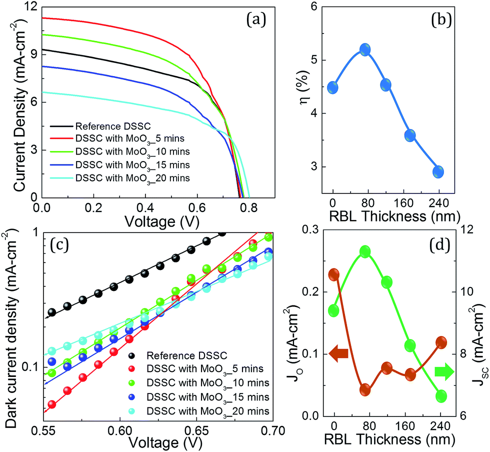 | ||
| Fig. 5 (a) J–V characteristics of the DSSCs employed MoO3 RBLs of different thickness showing a significant variation in JSC values and (b) thickness dependent variation in efficiency of DSSCs showing the possibility of achieving better performance for an optimum thickness of MoO3. (c) Semi-log plot of dark J–V characteristics in the medium forward bias region used for fitting to get JO and (d) thickness dependency of JO and JSC values. | ||
| DSSCs | JSC (mA cm2) | VOC (mV) | FF (%) | η (%) |
|---|---|---|---|---|
| Reference | 09.4 | 763 | 56.4 | 4.5 |
| 5 min MoO3 RBL | 11.3 | 766 | 59.4 | 5.2 |
| 10 min MoO3 RBL | 10.3 | 778 | 56.1 | 4.5 |
| 15 min MoO3 RBL | 08.3 | 776 | 56.7 | 3.6 |
| 20 min MoO3 RBL | 06.6 | 798 | 55.7 | 2.9 |
In general, dark saturation current density (JO) in DSSCs represents electronic quality of interfaces where the electron transport process is impeded by various recombination dynamics. Single diode model equation is given by JD = JOexp(qV/kT−1), where JD and JO are current density and saturation current under dark condition. The parameters q, V, k and T represent electronic charge, applied bias, Boltzmann constant and operating temperature. Dark current of a solar cell must be suppressed as much as possible to achieve improved solar cell parameters under illumination. Thus, it is essential to obtain JO as low as possible for DSSCs to get better η values. Fig. 5(c) shows semi-log plot of dark current density vs. voltage in a medium forward bias region (0.55–0.7 V). The highly linear current density data set in semi-log plot confirm that they are exponential in linear scale. Single diode model was used to fit to extract the JO and the values are shown in Fig. 5(d) with respect to RBL thickness values. We observed that 5 minutes deposited MoO3 suppressed the JO very efficiently than other MoO3 RBLs and the reference DSSC. The MoO3 layer controlled the JO value in the DSSC and resulted in lower JD which led to improved performance under illumination, particularly JSC values.
Nyquist and Bode phase plots of the reference and the DSSCs employing MoO3 RBLs are shown in Fig. 6(a and b) respectively. In general, the semicircles observed in kHz frequency range represent the charge transfer process at the TiO2/electrolyte interfaces in DSSCs. The semicircles obtained from the Nyquist plots assure that the MoO3 RBLs introduced at FTO/TiO2 interface significantly influenced the charge transfer process in the resulting DSSCs. The larger semicircles obtained for the DSSCs with 5 minutes coating of MoO3 RBL on FTO compared with reference DSSC confirming the recombination resistance between photo-generated electrons and holes at electrolyte is significantly improved due to the presence of MoO3. Also, the larger semicircle corresponding to the 5 minutes MoO3 RBL at FTO/TiO2 interface elucidates that charge transport process has been effectively facilitated by MoO3 compared to the reference DSSC. It is evident that electrolyte in DSSCs diffuse through the dye coated TiO2 nanoparticle layer to form the junction as a hole transport material candidate. However, this can lead to a direct electrical contact with FTO which is considered to be an electrical short. Nyquist plots obtained from the reference and DSSCs employing MoO3 RBLs show that such leaky charge transport pathways were effectively blocked by MoO3 RBLs. The Bode phase characteristics of the DSSCs shown in Fig. 6(b) depict that frequency values corresponding to the maximum phase angle shift towards lower values in case of DSSCs employing MoO3 RBLs compared to the reference DSSC. The low frequency shift observed in the DSSCs with MoO3 RBLs assures that charge transfer process occurs more efficiently compared with the reference DSSC. However, the optimum thickness value of MoO3 (5 minutes coating) resulting in higher JSC values compared to the reference DSSC while other DSSCs exhibit lower JSC values due to the increased thickness of MoO3 which impede charge transport while they establish an energy barrier for recombination between photo-electrons and holes.
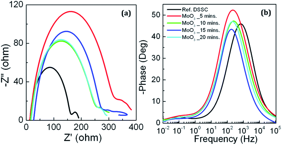 | ||
| Fig. 6 (a) Nyquist and (b) Bode phase characteristics of the reference DSSC along with the DSSCs employing MoO3 RBLs. Legends are common for both (a) and (b). | ||
TiCl4 is commonly used in DSSCs to treat the surface of mesoporous TiO2 and FTO. The present work introduces physical vapor deposition based MoO3 as an efficient RBL in DSSCs and the results are further compared with TiCl4 treated FTO in DSSCs. Fig. 7(a) shows J–V characteristics of two DSSCs with TiCl4 treated FTO electrodes showing very consistent photovoltaic characteristics under AM1.5 illumination. The J–V characteristics of the two DSSCs are represented as cell 1 and 2. This study utilized the same FTO, mesoporous TiO2, dye, electrolyte and Pt counter electrode used in the reference and MoO3 based DSSCs. The only difference is the TiCl4 treatment on FTO. The DSSC with FTO/TiCl4 showed JSC, VOC, FF and η of 5.5 mA cm−2, 808 mV, 71.2% and 3.2% respectively. This study observed only the VOC and FF were significantly improved by TiCl4 but overall performance remained lower than other DSSCs.
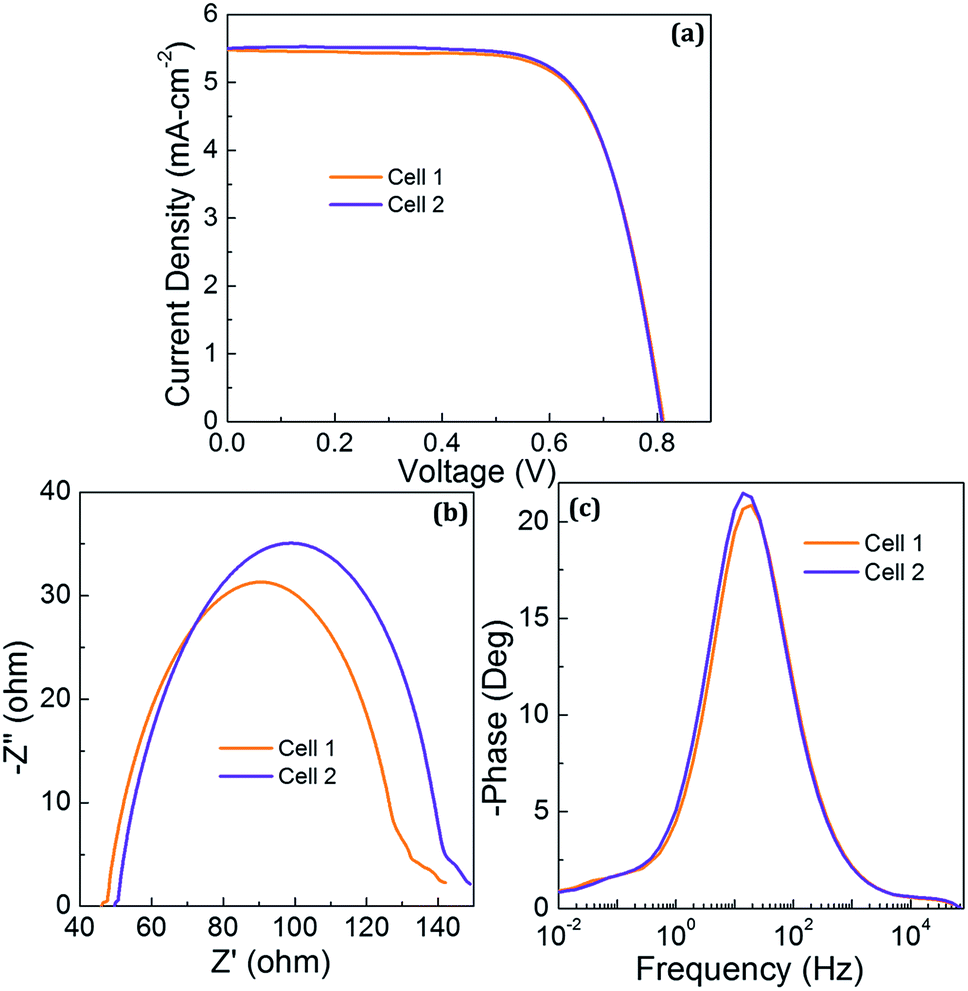 | ||
| Fig. 7 (a) J–V characteristics of the two DSSCs employed TiCl4 treatment on FTO (b) Nyquist and (c) Bode phase characteristics of the two DSSCs. | ||
Further, EIS studies were performed on the DSSCs with TiCl4 treated FTO to examine the Nyquist and Bode phase plots shown in Fig. 7(b and c) respectively. The semi-circles obtained from the DSSC with TiCl4 treated DSSCs shown in Fig. 7(b) are smaller than the one obtained from MoO3 RBL (5 minutes coating) assures the recombination resistance is smaller and this can be correlated to the difference in the blocking capability between TiCl4 and MoO3. The present study did not use any light scattering layers or surface treatment on mesoporous TiO2 to examine specifically the FTO/TiO2 interface. Thus, photovoltaic performance of the DSSCs reported in the present study is relatively lower compared to previous report.41
In general, incorporating MoO3 at FTO/TiO2 interface influences the charge transport at the FTO/TiO2 interface while acts as a barrier for recombination between photo-generated charge carriers and hole present in the electrolyte that diffuses through the mesoporous TiO2 nanoparticle layer. The charge transport characteristics can further be explained through the energy level alignment in the DSSCs with and without MoO3 RBLs. Fig. 8(a) shows the energy band diagrams of the FTO, TiO2, N719 and electrolyte before making the contact under thermal equilibrium (no exciton generation). Fig. 8(b) shows the alignment of energy levels of the FTO/TiO2/N719/electrolyte interfaces and major physical processes occur under illumination. Process 1, 2, 3, 4 and 5 represent exciton generation in N719, electron injection by N719 to EC of the TiO2, diffusion, collection at FTO and transport in the FTO respectively. The incoming solar photons enter into the DSSCs through FTO and TiO2. Optical bandgap values of FTO and TiO2 are 3.6 eV and 3.1 eV respectively which simply allow the visible energy spectral photons without any significant loss. Photonic interaction with N719 results in optical excitation and generates excitons as illustrated in process 1. The photo-generated electrons are injected into the EC of the TiO2 nanoparticles from the lowest unoccupied molecular orbital (LUMO) of N719. Diffusion of photo-electrons in the bulk of mesoporous TiO2 leads charge transport to reach the Fermi level (EF) of FTO electrode.
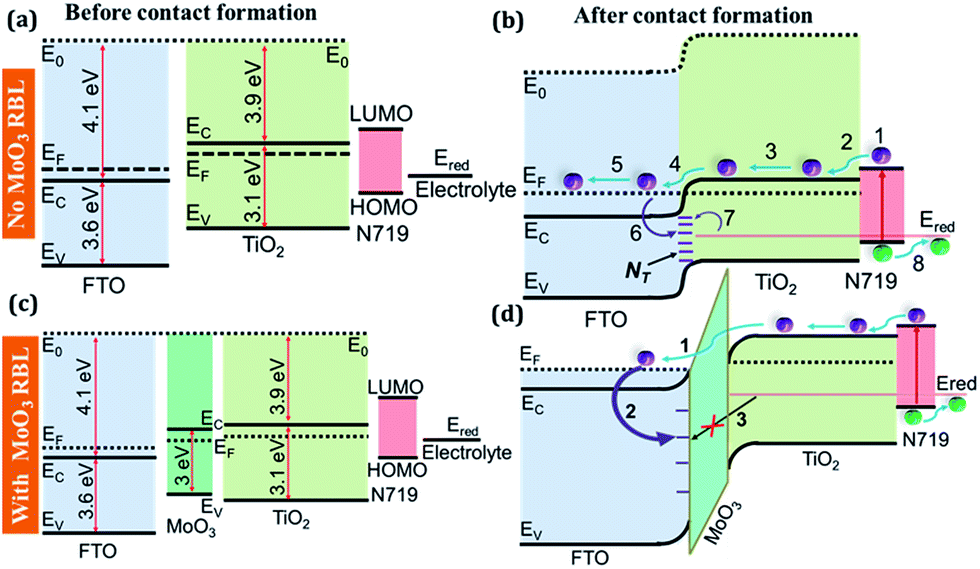 | ||
| Fig. 8 (a) Energy band diagrams of the FTO, TiO2, N719 and electrolyte before contact formation and (b) energy level alignment at FTO/TiO2/N719/electrolyte interfaces after contact formation. (c) Energy levels representing MoO3 RBL at FTO/TiO2 interface and (d) the alignment facilitating the charge transport through MoO3. | ||
Mesoporous TiO2 is preferred to adsorb more dye molecules; however, the porosity allows the liquid electrolyte to diffuse into the bulk to make TiO2/N719/electrolyte junction at which the electron–hole transport process starts after exciton dissociation. While the electrolyte diffuses into the bulk TiO2, the porosity of TiO2 offers a chance to make a direct electrical contact with the FTO which is considered to be an electrical short in DSSCs. Further, the defect states that are associated with FTO/TiO2 interface also actively participate in the electron capture process which can effectively trap photo-generated electrons at the FTO/TiO2 interface as represented by process 6 in Fig. 8(b). The electron capture process is expected to be followed by a hole capture process 7 as the electrolyte is in the vicinity of those defect states which capture photo-electrons. The two processes, electron–hole capture, lead to interfacial recombination mediated by the interfacial defects at FTO/TiO2 interface. Fig. 8(c) shows band diagrams of FTO, TiO2, N719 and electrolyte along with MoO3 RBL at FTO/TiO2 interface. Fig. 8(d) shows the energy level alignment at FTO/MoO3/TiO2/N719/electrolyte interfaces. From the illuminated J–V characteristics of the DSSCs, it is confirmed that MoO3 RBLs changed in FTO/TiO2 interface and thus the density and activity of the interfacial defects. The MoO3 layers acts as an energy barrier between photo-electrons and the hole present at the redox potential of the hole transport electrolyte. Thus, electron–hole recombination is significantly prohibited by incorporating MoO3 at FTO/TiO2 interface. It is expected that if MoO3 RBL establishes an energy barrier between the photo-electrons and the holes at the redox potential of the hole transport layer, then the JSC under illumination can be increased significantly by suppressing the interfacial recombination mediated by the defect states at FTO/TiO2 interface as shown in Fig. 8(d).
In general, process 1 is sensitive to the thickness of such interfacial layers and thus obtained results confirm the JSC decreased for further increase in the MoO3. Process 2 and 3 represent the electron and hole capture processes respectively. These two processes can happen effectively when there is no RBL and these two are suppressed by the RBL with an optimum thickness to facilitate the process 1 while 2 and 3 are prohibited.
4 Conclusions
Performance limiting interfacial recombination at FTO/TiO2 interface can be suppressed by coating MoO3 layers on FTO by reactive DC sputtering. There is no significant optical loss in MoO3 films, even for 20 minutes deposition. The 15% enhancement in the performance of DSSC is attributed to the effect of MoO3 on electron–hole capture processing which were significantly controlled for an optimum growth of 5 minutes. Further increase in the thickness of MoO3 impedes the charge transport process at FTO/TiO2 interface and affects the DSSC performance. The presented work leads to the establishment of defect engineered material interfaces to progress the research and developmental works in DSSCs.Conflicts of interest
The authors declare no conflict of interest.Acknowledgements
We thank Department of Science and Technology, Government of India for financial support through Solar Energy Research Initiative. The authors would like to thank Dr Dhamodaran Santhanagopalan for providing Mo sputter target through his Ramanujan Fellowship and AEPL for PVD cluster facility.References
- M. Wright and A. Uddin, Sol. Energy Mater. Sol. Cells, 2012, 107, 87–111 CrossRef CAS.
- S. Günes and N. S. Sariciftci, Inorg. Chim. Acta, 2008, 361, 581–588 CrossRef.
- P. Poudel and Q. Qiao, Nanoscale, 2012, 4, 2826–2838 RSC.
- B. O'regan and M. Grfitzel, Nature, 1991, 353, 737–740 CrossRef.
- J. M. Kroon, N. J. Bakker, H. J. P. Smit, P. Liska, K. R. Thampi, P. Wang and S. M. Zakeeruddin, et al., Prog. Photovoltaics, 2007, 15, 1–18 CAS.
- T. G. Deepak, G. S. Anjusree, S. Thomas, T. A. Arun, S. V. Nair and A. S. Nair, RSC Adv., 2014, 4, 17615–17638 RSC.
- R. Harikisun and H. Desilvestro, Sol. Energy, 2011, 85, 1179–1188 CrossRef CAS.
- N. Kato, K. Higuchi, H. Tanaka, J. Nakajima, T. Sano and T. Toyoda, Sol. Energy Mater. Sol. Cells, 2011, 95, 301–305 CrossRef CAS.
- A. Hinsch, J. M. Kroon, R. Kern, I. Uhlendorf, J. Holzbock, A. Meyer and J. Ferber, Prog. Photovoltaics, 2001, 9, 425–438 CAS.
- M. I. Asghar, K. Miettunen, J. Halme, P. Vahermaa, M. Toivola, K. Aitola and P. Lund, Energy Environ. Sci., 2010, 3, 418–426 CAS.
- D. Kuang, C. Klein, S. Ito, J.-E. Moser, R. Humphry-Baker, N. Evans, F. Duriaux, C. Graetzel, S. M. Zakeeruddin and M. Grätzel, Adv. Mater., 2007, 19, 1133–1137 CrossRef CAS.
- P. Wang, S. M. Zakeeruddin, R. Humphry-Baker, J. E. Moser and M. Grätzel, Adv. Mater., 2003, 15, 2101–2104 CrossRef CAS.
- M. Grätzel, Prog. Photovoltaics, 2000, 8, 171–185 Search PubMed.
- K. Shankar, G. K. Mor, H. E. Prakasam, S. Yoriya, M. Paulose, O. K. Varghese and C. A. Grimes, Nanotechnology, 2007, 18, 065707 CrossRef.
- S. V. Nair, A. Balakrishnan, K. R. V. Subramanian, A. M. Anu, A. M. Asha and B. Deepika, Bull. Mater. Sci., 2012, 35, 489–493 CrossRef CAS.
- B. Tan and Y. Wu, J. Phys. Chem. B, 2006, 110, 15932–15938 CrossRef CAS PubMed.
- E. Ghadiri, N. Taghavinia, S. M. Zakeeruddin, M. Grätzel and J.-E. Moser, Nano Lett., 2010, 10, 1632–1638 CrossRef CAS PubMed.
- D. Chen, F. Huang, Y.-B. Cheng and R. A. Caruso, Adv. Mater., 2009, 21, 2206–2210 CrossRef CAS.
- S. Agarwal, M. Kevin, A. S. W. Wong, C. K. N. Peh, V. Thavasi and G. W. Ho, ACS Appl. Mater. Interfaces, 2010, 2, 1844–1850 Search PubMed.
- Z.-Q. Li, Y. Ding, L.-E. Mo, L.-H. Hu, J.-H. Wu and S.-Y. Dai, ACS Appl. Mater. Interfaces, 2015, 7, 22277–22283 CAS.
- M. Safdari, P. W. Lohse, L. Häggman, S. Frykstrand, D. Högberg, M. Rutland and R. A. Asencio, et al., RSC Adv., 2016, 6, 56580–56588 RSC.
- H. Cheema and J. H. Delcamp, ACS Appl. Mater. Interfaces, 2017, 9, 3050–3059 CAS.
- A. Yella, S. Mathew, S. Aghazada, P. Comte, M. Grätzel and M. K. Nazeeruddin, J. Mater. Chem. C, 2017, 5, 2833–2843 RSC.
- J. Van de Lagemaat and A. J. Frank, J. Phys. Chem. B, 2000, 104, 4292–4294 CrossRef CAS.
- Q. Yu, Y. Wang, Z. Yi, N. Zu, J. Zhang, M. Zhang and P. Wang, ACS Nano, 2010, 4, 6032–6038 CrossRef CAS PubMed.
- A. Burke, S. Ito, H. Snaith, U. Bach, J. Kwiatkowski and M. Grätzel, Nano Lett., 2008, 8, 977–981 CrossRef CAS PubMed.
- N. Huang, Y. Liu, T. Peng, X. Sun, B. Sebo, Q. Tai, H. Hu, B. Chen, S.-S. Guo and X. Zhao, J. Power Sources, 2012, 204, 257–264 CrossRef CAS.
- B. Bills, M. Shanmugam and M. Farrokh Baroughi, Thin Solid Films, 2011, 519, 7803–7808 CrossRef CAS.
- S. Lee, J. H. Noh, H. S. Han, D. K. Yim, D. H. Kim, J.-K. Lee, J. Y. Kim, H. S. Jung and K. S. Hong, J. Phys. Chem. C, 2009, 113, 6878–6882 CAS.
- W.-Q. Zhou, Y.-M. Lu, C.-Z. Chen, Z.-Y. Liu and C.-B. Cai, J. Inorg. Mater., 2011, 26, 819–822 CrossRef CAS.
- H. Choi, C. Nahm, J. Kim, J. Moon, S. Nam, D.-R. Jung and B. Park, Curr. Appl. Phys., 2012, 12, 737–741 CrossRef.
- T. Matsushima, Y. Kinoshita and H. Murata, Appl. Phys. Lett., 2007, 91.25, 253504 CrossRef.
- H. Lee, S. W. Cho, K. Han, P. E. Jeon, C.-N. Whang, K. Jeong, K. Cho and Y. Yi, Appl. Phys. Lett., 2008, 93, 279 Search PubMed.
- J. Meyer and A. Kahn, J. Photonics Energy, 2011, 1, 011109 CrossRef.
- D. Mutschall, K. Holzner and E. Obermeier, Sens. Actuators, B, 1996, 36, 320–324 CrossRef CAS.
- K. Gesheva, A. Kostadinka and T. Ivanova, Chem. Vap. Deposition, 2006, 12, 231–238 CrossRef CAS.
- F. Cheng, Y. Wu, Y. Shen, X. Cai and L. Li, RSC Adv., 2017, 7, 37952–37958 RSC.
- C. Julien, A. Khelfa, O. M. Hussain and G. A. Nazri, J. Cryst. Growth, 1995, 156, 235–244 CrossRef CAS.
- O. M. Hussain, K. S. Rao, K. V. Madhuri, C. V. Ramana, B. S. Naidu, S. Pai, J. John and R. Pinto, Appl. Phys. A: Mater. Sci. Process., 2002, 75, 417–422 CrossRef CAS.
- A. K. Prasad, D. J. Kubinski and P. I. Gouma, Sens. Actuators, B, 2003, 93, 25–30 CrossRef CAS.
- S. Ito, T. N. Murakami, P. Comte, P. Liska, C. Grätzel, M. K. Nazeeruddin and M. Grätzel, Thin Solid Films, 2008, 516, 4613–4619 CrossRef CAS.
| This journal is © The Royal Society of Chemistry 2017 |