
 Open Access Article
 This Open Access Article is licensed under a
 Creative Commons Attribution 3.0 Unported Licence
Modulating the electronic and magnetic properties of graphene
Salma Nigara,
Zhongfu Zhou *abcd,
Hao Wang*ab and
Muhammad Imtiaze
*abcd,
Hao Wang*ab and
Muhammad Imtiaze
aSchool of Material Science and Engineering, Shanghai University, Shanghai 200444, P. R. China
bState Key Laboratory of Advanced Special Steel, Shanghai University, Shanghai 200072, P. R. China. E-mail: z.zhou@shu.edu.cn
cKey Laboratory of Material Microstructures, Shanghai University, Shanghai 200444, P. R. China
dDepartment of Physics, Aberystwyth University, Aberystwyth SY23 3BZ, UK
eState Key Laboratory of Metal Matrix Composites, Shanghai Jiao Tong University, 800 Dongchuan Road, Shanghai 200240, P. R. China
First published on 7th November 2017
Abstract
Graphene, an sp2 hybridized single sheet of carbon atoms organized in a honeycomb lattice, is a zero band gap semiconductor or semimetal. This emerging material has been the subject of recent intensive research due to the novelty of its structural, electronic, optical, mechanical, and magnetic properties. Due to these properties, graphene is a favorable material for the fabrication of electronic devices, transparent electrodes, spintronics devices, and a growing array of several other applications that explore the potential of this marvelous material. However, the lack of intrinsic band gap and nonmagnetic nature of graphene limit its practical applications in the widely expanding field of carbon-based devices. To take advantage of the hidden potential of this material, numerous techniques have been developed to tailor its electronic and magnetic properties. These methods include the mutual interaction between graphene layer and its substrate, doping with surface adatoms, substitutional doping, vacancy creation, and edges and strain manipulation. Herein, an overview of recently emerging innovative techniques adopted to tailor the electronic and magnetic properties of graphene is presented. The limitations, possible directions for future research and applications in diverse fields of these methods are also mentioned.
1. Introduction
Graphene is an sp2 two dimensional honeycomb lattice of carbon atoms comprising two atoms per unit cell.1 Its two bands, π and π*, emerge from the pz orbitals and meet at six points in k-space known as Dirac points, which are at the edges of the Brillouin zone (BZ) K and K′; thus, graphene is a zero-gap semiconductor or semimetal. Its linear energy versus momentum dispersion with the Fermi energy (EF) at the Dirac point (ED) leads to remarkable properties, such as ambipolar field effects,1 high carrier mobility1,2 and room temperature quantum hall effects.3 Due to its astonishing electronic, optical, thermal, magnetic, mechanical and electrochemical properties, graphene has attracted immense interest in diverse fields of research, such as electronics,4 optoelectronics,4,5 energy conversion and storage devices,6,7 sensors8,9 and biomedicine.10,11 However, despite the above mentioned properties, the lack of intrinsic band gap and nonmagnetic nature of pristine graphene limit the broader practical applications of this material. To explore the inherent capabilities of graphene for practical applications, several techniques have been developed to tailor its electronic and magnetic properties. As the zero-gap band structure of graphene is attributed to the sublattice symmetry of its hexagonal structure, breaking of the sublattice symmetry by local changes in the lattice, such as by interaction of a layer of graphene with its substrate, surface doping with adatoms, substitutional doping, vacancy creation, and graphene edges and strain manipulation, are innovative methods to tailor the intrinsic properties of graphene. Herein, we present an overview of the recent tremendous efforts devoted to tailoring the intrinsic electronic and magnetic properties of graphene.In this review, we have organized our discussion of the modulating techniques into five sections. Section 2 specifically covers modulation during the growth of graphene on different substrates including silicon carbide (SiC), silicon (Si), silicon dioxide (SiO2), hexagonal boron nitride (h-BN) and various transition metal (TM) surfaces. In Section 3, we discuss the adsorption of various adatoms on the surface of graphene. These interactions lead to band gap opening and confer magnetic properties on graphene. The discussion includes metal and non-metal adatom adsorption as well as hydrogenation and halogenation of graphene. Section 4 contains a brief discussion of the modulation of electronic and magnetic properties of graphene by substitution or heteroatom doping. This section includes groups IIIA, IVA, VA, and VIA, transition metals, and two-atom substitution or dual-doping of graphene. In Section 5 of the review, we discuss modulation by creating vacancies in graphene. Section 6 contains a brief discussion of the edges (size confinement) of graphene and the application of strain to graphene. The effects of edges and strain on the electronic, magnetic and chemical properties of graphene are discussed in detail. Every section contains a brief discussion of the modulation of the electronic structure and magnetic properties of graphene. The synthesis, theoretical modeling and remarkable applications of all the mentioned methods are discussed in their respective sections. Furthermore, each section is accompanied by concluding remarks.
2. Modulation via different substrates and their applications
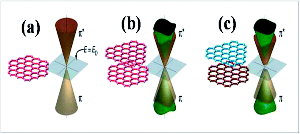
Experimental techniques and theoretical models developed to explore the nature of epitaxial graphene reveal that the substrate can tune the electronic properties of graphene due to the exchange of charge between graphene and the substrate.12,13 The graphene substrate bonding phenomenon and the resulting structural and electronic properties are highly important when examining the quality and properties of fabricated graphene. It has been shown that two layers of graphene interact weakly. However, the bonding between the first layer of graphene and its substrate induces changes in the structural lattice of graphene. These structural changes may facilitate the creation of interface or buffer layer (BL) graphene, which exhibits electronic characteristics distinct from isolated sheets of graphene.14Graphene bilayer is a zero band semimetal due to the contact of its two π-bands at the Dirac points, as shown in Fig. 1(b). Bilayer graphene is similar to monolayer graphene (Fig. 1(a)), except that it demonstrates parabolic π-dispersion compared to linear dispersion in the case of the monolayer.15 The intrinsic band structure of graphene is dependent on the sublattice symmetry. The breaking of lattice symmetry results in band gap opening at the Dirac points. The lateral in-plane symmetry can be broken if the hexagonal layer structure consists of two nonequivalent atoms or two stacked layers in the Bernal stacking form, where the two layers are rotated with respect to each other. This type of asymmetry, which is depicted in Fig. 1(c), results in band gap opening.15,16 Different substrates such as SiC, Si, SiO2, h/BN and various metal surfaces are utilized for the growth of graphene.
 | ||
| Fig. 1 Representation of the electronic structures of graphene: (a) single layer, (b) symmetric double layer, and (c) asymmetric double layer. Reproduced with permission.15 © 2006 American Association for the Advancement of Science. | ||
2.1 SiC substrate
Different experimental and theoretical strategies have been used to grow graphene epitaxially on SiC (4H and 6H-SiC substrates). For graphene growth, SiC is an important substrate14,17,18 due to its facile integration into present industrial techniques used in the electronics industry. However, its high cost limits its use in large scale production of graphene. Graphene has been grown on both faces of SiC, i.e. the Si-terminated (0001) face and the C-terminated (000![[1 with combining macron]](https://www.rsc.org/images/entities/char_0031_0304.gif) ) face.14,18 However, the characteristics of the graphene structures grown on both faces of SiC are different. Theoretical studies of the structural and electronic properties of graphene layers grown on Si- and C-terminated 1 × 1-6H-SiC substrates have confirmed the metallic and semiconducting nature of each, respectively. The first layer, known as the buffer layer, acts as a separator between the substrate and the upper layers and prevents their interaction. The buffer layer establishes strong covalent bonds with the substrate, which renders its structural and electronic behavior. The application of stretch to prevent mismatched graphene and SiC lattices does not affect the electronic structure of graphene except for its Dirac Fermi velocity and band width. The Fermi conical points and band structure are only characteristic of the second layer of graphene.14 The n-type doping and band gap opening in the synthesis of a bilayer on a SiC surface is attributed to the breaking of symmetry between the two lattices of graphene, caused by the production of a dipole electric field between the depletion layer of SiC and charge accretion on the graphene layer that is closest to the substrate.15
) face.14,18 However, the characteristics of the graphene structures grown on both faces of SiC are different. Theoretical studies of the structural and electronic properties of graphene layers grown on Si- and C-terminated 1 × 1-6H-SiC substrates have confirmed the metallic and semiconducting nature of each, respectively. The first layer, known as the buffer layer, acts as a separator between the substrate and the upper layers and prevents their interaction. The buffer layer establishes strong covalent bonds with the substrate, which renders its structural and electronic behavior. The application of stretch to prevent mismatched graphene and SiC lattices does not affect the electronic structure of graphene except for its Dirac Fermi velocity and band width. The Fermi conical points and band structure are only characteristic of the second layer of graphene.14 The n-type doping and band gap opening in the synthesis of a bilayer on a SiC surface is attributed to the breaking of symmetry between the two lattices of graphene, caused by the production of a dipole electric field between the depletion layer of SiC and charge accretion on the graphene layer that is closest to the substrate.15
A band gap of 0.26 eV (Fig. 2(b)) is observed during synthesis of graphene on SiC; this originates from the breaking of symmetry of the graphene lattice.12 Fig. 2(b) presents the angle resolved photoemission spectroscopy (ARPES) results. The intensity is calculated as a function of both the energy and the momentum along one point, i.e. K of the Dirac point in Fig. 2(a). The energy for the presumed Dirac point that is taken mid-way between the valence band maximum and conduction band minimum is nearly 0.4 eV below the Fermi energy. This confirms a band gap opening at the K point.12 Theoretically, it is suggested that along with asymmetry of the buffer layer, Stone Wales (SW) defects in graphene layers also induce a band gap,19 which is in agreement with the experimental results.12 The band gap was found to increase with decreasing number of layers.12,19
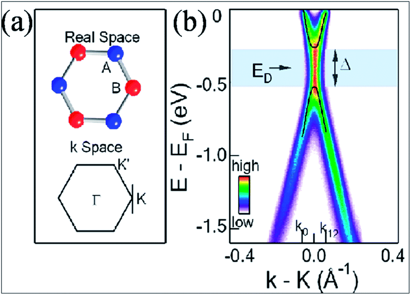 | ||
| Fig. 2 (a) Structures of graphene in the real and momentum spaces. (b) ARPES intensity plot indicating the gap opening in single layer graphene at point K in the momentum space. Reproduced with permission12 © 2007 Nature Materials. | ||
Graphene grown on 4H-SiC sublattices showed rotation of graphene layers relative to each other instead of AB stacking.20,21 The electronic structure produced by this method for a system of multilayer graphene resembled that of an isolated graphene layer. Moreover, the electronic properties of graphene on the SiC surface can be enhanced via adsorption or intercalation of different elements.22 SiC-grown graphene is a potential material in the fabrication of high quality field effect transistors (FETs). The highest cutoff radio frequency of 100 GHz was reported for a graphene FET fabricated on a SiC substrate;23 this value reached 300 GHz after improvement of the quality of graphene.24 In addition to the cutoff frequency, the oscillation frequency of the transistors attained a maximum value of 70 GHz for C-face-grown graphene using an appropriately high k dielectric T-gate.25 Thermally stable operation has been demonstrated for integrated circuit elements designed using graphene grown on SiC.26
Opposite conductance variation has been observed for graphene epitaxially grown on the C and Si-faces of 6H-SiC. Si-face-grown graphene showed a 10% reduction in conductance at 18 ppm of nitrogen dioxide (NO2), while an increase of 4.5% was reported for C-face-grown graphene. This behavior is related to the different doped states, i.e. Si-face (p-type) and C-face (n-type), of the two graphene materials.27 Graphene is a good sensing material due to its large surface area and good adsorption capacity. Gas sensing tests of graphene grown on SiC determined its ability as a sensor for the detection of NO2 gas molecules.28 The better electrochemical sensing performance of anodized epitaxially grown graphene is attributed to the increase in the number of defects and oxygen functional groups created by the anodizing potential.29 Moreover, chemical vapor deposition (CVD) is a novel method for graphene preparation on metal substrates30 and on SiC(0001).31 Owing to the advantages of low temperature growth, production of good quality graphene layers and weaker interaction with the substrate, CVD-grown graphene has been proven to have excellent potential in various fields, such as electrochemical devices,32 electronic transistors,33 corrosion inhibiting coatings34 and transparent electrodes.35
2.2 Si/SiO2 substrate
Scanning tunneling microscopy (STM) images show perturbation in the structure of clean graphene grown on SiO2 substrate, which confirms changes in the electronic states of graphene.36 The theoretically predicted band gap opening in graphene at the surface of SiO2 substrate is attributed to the inherent elemental properties of the substrate.37 Si/SiO2 substrate-supported graphene was found to be doped.38 However, the nature of doping induced by the SiO2 substrate is proposed to be dependent on the existence of contact potential differences between the layer of graphene and its substrate because these differences specify the direction of a dipole that is produced due to mutual charge transfer between the graphene layer and the substrate.38 Combined experimental and theoretical investigations have been conducted on the interaction of graphene with clean Si(100) and hydrogen-passivated silicon (Si(100)/H) substrates. These investigations revealed that the electronic properties of graphene on Si(100)/H are not modified due to the absence of both bonding and sharing of charge between the graphene flakes and the Si surface. However, modification of the electronic properties of graphene on a clean Si(100) surface occurs due to the formation of covalent bonds between Si and C atoms.39 Single layer graphene grown on SiO2 substrate by the CVD method showed poor electrochemical response compared to both quasi-graphene and highly ordered pyrolytic graphite (HOPG). The better electrochemical responses of quasi-graphene and HOPG are attributed to their large extent of edge plane coverage, numerous defects and larger number of layers.402.3 BN substrate
In contrast to SiO2 substrate, STM images of graphene on the surface of hexagonal boron nitride showed an excellent flat pattern of the graphene layer.41 Experimentally, no band gap opening is observed for graphene grown on BN substrate.42 However, some theoretical calculations that did not account for both lattice mismatch and relative rotation predicted a substrate-induced band gap in hexagonal graphene on BN substrate.43,44 For graphene on the cubic BN(111) surface,44 a gap appeared due to the breaking of equivalence between the sublattices of graphene. This is because of the different chemical environments of the two sublattices, which are positioned at different locations on the BN lattice. This band gap opening is also reported in ref. 43. The density of states (DOS) and band structure of graphene on h-BN are shown in Fig. 3(a) and (b), respectively. The opening of the band gap (53 meV) is related to the induction of inequivalence between the two lattices of graphene grown on h-BN. In this configuration, one carbon of graphene is placed above the boron atom, while the second is placed in the central position of the BN ring.43 In another study of graphene on BN substrate, the presence of a band gap was attributed to the structural relaxation of graphene atoms.13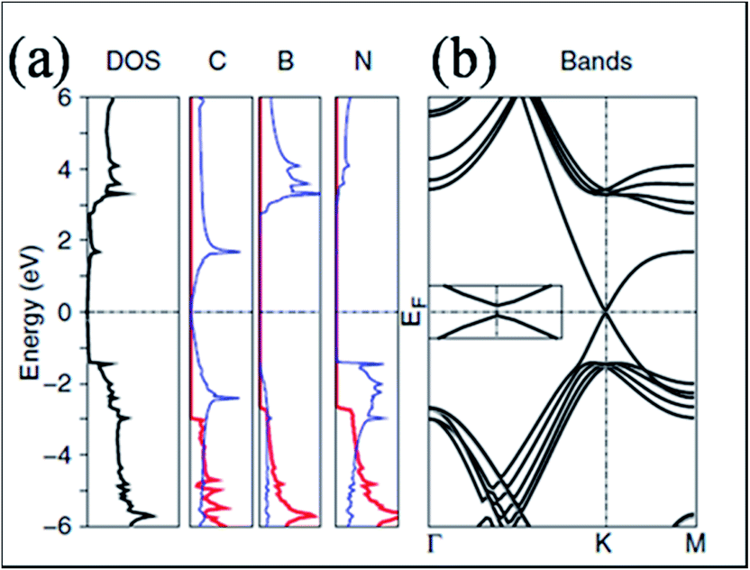 | ||
| Fig. 3 (a) Total DOS for a graphene layer on h-BN and the projected density of states for C, B and N on the p states in plane (red lines) and out of plane (blue lines), and (b) respective band structure plot of graphene on h-BN, indicating gap opening. Reproduced with permission.43 © 2007 American Physical Society. | ||
2.4 Transition metal substrates
For the growth and deposition of graphene on metal surfaces, the fcc(111) and hcp(0001) surfaces of d state transition metals are efficient substrates. The successful growth of graphene on TM surfaces, including Ru(0001),45 Rh(111),46 Pd(111),47 Ir(111)48 and Pt(111),49 has been studied. The electronic properties of graphene showed a significant change after its chemisorption on metal substrates, such as the (111) surfaces of Co, Ni, Ti and Pd. However, calculations revealed that the electronic properties of graphene physisorbed on Al, Cu, Ag, Au and Pt surfaces are preserved, as shown in Fig. 4.50,51 The usual conical electronic structure of graphene is expected to be sustained during its interaction with the substrate. However, the shifting of its Fermi level with respect to the Dirac point and their coincidence results in p-type or n-type doping. This shift of the Fermi level is dependent on the transfer of charge between the substrate and graphene. The distribution of charge at the metal–graphene interface is governed by both the electronic charge transfer and by mutual chemical interaction between graphene and the metal.50 The results of STM and DFT studies for the growth of graphene on the Co(0001) surface revealed that perturbation was produced in its electronic structure, which is attributed to coupling between graphene π and cobalt d-electrons.51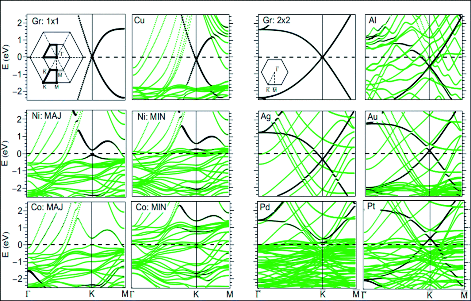 | ||
| Fig. 4 Band structure of isolated graphene shown in the first and third top panels, calculated using 1 × 1 and 2 × 2 super cells (insets: two-dimensional BZ of 1 × 1 and 2 × 2 super cells). The band structure plots correspond to graphene adsorbed on Au, Pt, Cu, Ag, Al, Pd, Ni, and Co(111) surfaces. The contribution from the pz character of carbon is shown by the blackness of the bands. The pristine graphene intrinsic conical points present at the crossing of the bands at K with dominant pz character are not disturbed by physisorption of Au, Pt, Cu, Ag, and Al. Meanwhile, through the chemisorptions of Pd, Ni, and Co, the conical points disappear and the bands show mixed character. MIN and MAJ respectively denote the majority and minority-spin polarized bands of graphene on Ni and Co. The Fermi level is at zero energy. Reproduced with permission.50 © 2009 American Physical Society. | ||
The surface of Ni(111), a 3d metal, is a suitable substrate for graphene growth due to its very low lattice mismatch of 1.3%.52 Its use is limited due to alteration of the graphene Dirac cone during growth. However, the linear dispersion of pristine graphene is preserved by intercalation of alkali metals53 and noble metals54 between graphene and its Ni(111) substrate. The absence of π surface plasmon excitation indicated that the graphene band structure is influenced by interactions with the Ni substrate.55 It has been shown that intercalation of Bi56 and Co57 on graphene/Ir(111) leads to doping, band gap opening,56,57 and induction of spin polarization in the graphene layer.57 Graphene grown on Ni58 and Cu59 substrates has been applied in flexible and transparent electrodes.59 At room temperature, a high electron mobility of 4050 cm2 V−1 s−1 was recorded for a dual-gated FET that was fabricated on a Si/SiO2 substrate using graphene grown on Cu foils.60
2.5 Concluding remarks and future outlook
In contrast to weak graphene–substrate interactions, which preserve the intrinsic properties of graphene, a strong interaction between graphene and its substrate leads to doping, band gap opening and induction of magnetism in non-magnetic graphene. The structural and electronic properties of graphene grown on SiC have been found to depend on the polytype and polarity of the substrate. The commonly used polytypes of SiC substrate for graphene growth are hexagonal 4H and 6H. Graphene grown on both the C- and Si-terminated faces of SiC exhibits distinct features. However, in both cases, surface reconstruction results in the formation of an interface layer known as the “buffer layer” whose observed electronic properties are distinct from those of the pristine graphene layer. Due to the strong interactions of graphene with substrates, it is difficult to transfer grown graphene to other substrates for commercial fabrication of flexible or bendable devices. However, devices can be directly fabricated on SiC substrate. Due to the ease of the fabrication method of these devices, SiC substrate has potential in the large scale production of graphene and graphene-based electronics. Lattice mismatch and surface roughnesses pose many challenges in the growth of high quality graphene on SiO2 and SiC substrates.Band gap opening via breaking of the sublattice symmetry has been observed in graphene grown on h-BN substrate. BN is a viable insulating substrate for the fabrication of graphene-based devices due to its advantages of (i) similar dielectric properties to SiO2 (ii) and lower effect on the mobility of charge carriers of the grown graphene due to the presence of fewer charge impurities. The flat surface of h-BN and the lack of dangling bonds at the substrate–graphene interface are the key factors for improvement of the charge carrier mobility of graphene. Graphene shows inadequate on/off switching properties in FETs, which is a consequence of its gapless electronic behavior; this may be improved by growing graphene on h-BN. Graphene grows more readily on metal surfaces than on the SiC substrate. The interaction between graphene and the underlying metal substrate is remarkable. Graphene shows both physisorption and chemisorption on different metal substrates. The band gap opening and magnetic properties of graphene on metal surfaces can be further enhanced via intercalation of different metals or non-metals between the graphene–substrate interface. For better demonstration of the electronic and magnetic nature of graphene and their alteration on different substrates, further experimental and theoretical investigations are still required. Furthermore, novel and inexpensive methods are currently necessary to modulate the band gap and magnetism of graphene for its future commercial use.
3. Modulation via adsorption of different atoms on the surface of graphene and applications
3.1 Modulation via metals and non-metals
In addition to the intrinsic properties of pristine graphene, numerous theoretical and experimental researchers have focused on adsorbing metal and nonmetal impurities on graphene with the aim of expanding the myriad applications of graphene in device fabrication. Graphene doping may be divided into two categories: (a) electrical doping61 and (b) chemical doping.62 Chemical doping covers two major areas: (a) doping via adatoms or surface charge doping63 and (b) substitutional doping.64,65The adsorption of various chemicals, including alkyl metals,63,66 alkaline earth metals,67 transition metals,63,68 noble metals,69 nonmetals70 and clusters,71 on graphene continues to grow rapidly; this increases its potential in a range of applications such as catalysis72 and spintronics.73 The growth morphologies and thermal stabilities of adatoms, as well as the interaction of metal adatoms with each other and with graphene surfaces, have been found to be different for different adatoms. Metal adsorption on the surface of graphene induces lattice distortion, an electric dipole moment and a spin polarized magnetic moment. The phenomena of distortion and induced electric and magnetic dipole moments in graphene are different for different adsorbed atoms. The distortion patterns for group I–IV metals are nearly identical. The structural distortion in graphene evoked through the adsorption of transition and rare earth metals is larger than that produced by the adsorption of group I–IV metals.66,74 The electric dipole moment is found to be dependent on the magnitude of charge exchange between adatoms and the graphene substrate. Greater charge transfer is found to induce a larger electric dipole moment. However, converse behavior is shown by adatoms of Al, Ca and Yb.66,74
The hexagonal surface of graphene contains different favorable sites for adsorption. The hollow site (H) is the center of a hexagon, the bridge site (B) is the midpoint of a carbon–carbon bond and the top site (T) is directly above a carbon atom. The positions of the three sites are depicted in Fig. 5(a).63 Alkali and alkaline earth metals are good sources of n-type doping of graphene63,67,75 due to their ability to easily evolve electrons without destroying the electronic properties of graphene. The adsorption of potassium (K) atom on both graphene and carbon nanotubes (CNTs) demonstrates the presence of long range electrostatic interactions between K and graphene. Moreover, the energy of the adsorbed K is dependent on the surface curvature and chirality of the CNTs.74 Experimental and theoretical studies have elucidated that K atoms behave as electron donors.63,75,76 Band structure studies of K-adsorbed graphene reveal a shift of the Fermi level above the Dirac point; this confirms the n-type doping of graphene, as shown in Fig. 5(b). Furthermore, it has been found that the occupied 4s1 electronic state of an isolated K atom, shown in Fig. 5(c), becomes empty due to the adsorption of K atoms on graphene (marked as A in Fig. 5(b)). However, the wave functions of the highly occupied levels above the graphene Dirac point (marked as B in Fig. 5(b)) are delocalized over the carbon atoms of graphene, confirming the presence of free electrons (Fig. 5(d)). These results suggest that n-type doping is due to electronic charge transfer from the K adatoms to the graphene surface. The integration of pristine graphene DOS with the Fermi level of K-adsorbed graphene confirmed the transfer of one electron per adsorbed adatom.
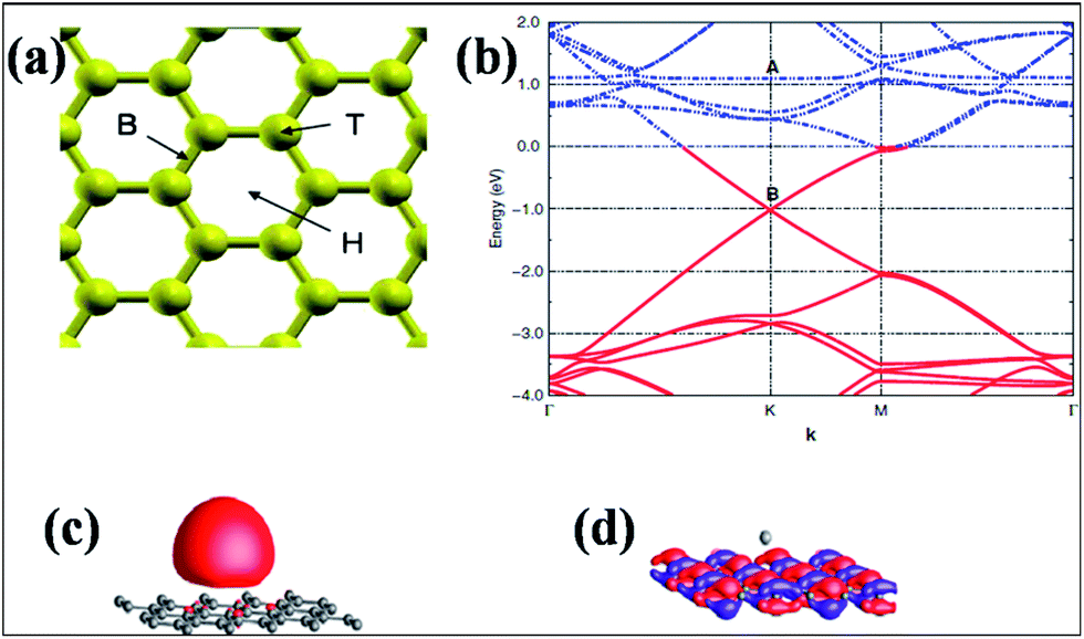 | ||
| Fig. 5 (a) Adsorption sites on the surface of graphene: hollow (H), bridge (B), and top (T). Reproduced with permission.63 © 2008 American Physical Society. (b) Band structure representation of K-adsorbed graphene in the vicinity of the Fermi energy. The Fermi level is set to zero. Occupied states are shown by red lines, while empty levels are shown by blue lines. The unoccupied bands of pristine graphene around B became occupied due to the adsorption. (c, d) Representations of the real part of the wave functions of the electronic levels, marked as A and B in panel (b). The wave function of the level marked as A is localized on the K atom, while the wave function of the occupied level, which is marked as B, is delocalized over the hexagonal graphene layer. Reproduced with permission.75 © 2010 American Physical Society. | ||
In contrast to the n-type doping induced by electropositive adatoms, p-type doping of epitaxially grown graphene on SiC by adsorption of electronegative elements such as Bi, Sb77 and Au77,78 has been observed. The resulting band structures of graphene without adatoms (Fig. 6(a)) and with adatoms (Bi atoms) in Fig. 6(b–d) are presented for comparison. This image reveals n-type doping for undoped epitaxial graphene, while graphene shows p-type doping by increasing the concentration of Bi atoms on the surface of graphene. This p-type doping shifts the Dirac point (420 meV) into the valence band (occupied states). However, the linear dispersion of the valence and conduction bands is unaltered. The p-type doping of graphene is also observed in the case of Au adsorption. A narrower band is obtained for graphene doped with Au compared to graphene doped with Bi or Sb.77 This shift of the Dirac point with increasing concentration of dopant has been recorded for transition metal adatoms on the surface of graphene using the molecular beam epitaxy (MBE) technique.79 Depending on its coverage concentration, Pt can lead to n- or p-type doping. Furthermore, work function differences and interfacial dipoles also play major roles in the doping process.
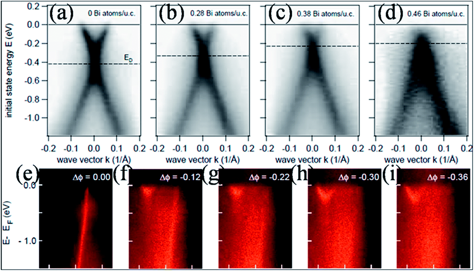 | ||
| Fig. 6 Experimental band structures of an epitaxial (a) pristine graphene layer and (b–d) graphene doped with increasing concentrations of bismuth atoms. Reproduced with permission.77 © 2008 American Chemical Society. (e–i) The progressive change in the π band structure of single layer graphene with increasing dose of Na at 85 K. The linear π band quickly decays both in intensity and in bandwidth, while a new parabolic band appears. Reproduced with permission.85 © 2009 American Physical Society. | ||
Group (I–III) adatoms show ionic bonding and minimal changes to the electronic structure of graphene. However, transition metal atoms with d valence electrons, group IV elements and noble metals establish covalent bonds with the graphene surface and lead to perturbations in the hybridization of graphene.63,67,80 For different concentrations of Li atoms adsorbed on graphene sheets,81,82 it is revealed that the increase of Li adatoms showed a tendency to form clusters on the graphene surface. For single layer graphene, the energetically supportive Li/C ratio was calculated to be less than 1/6.82 The high concentration of Li adatoms significantly contributes to the electronic properties due to the formation of chemical bonding; however, no such evidence is found for low concentrations except for ionic characteristics and charge transfer to the graphene surface.81 The graphene electronic structure is found to be tuned due to both strong hybridization between adatoms and the graphene π and π* orbitals and charge transfer from the adatoms to the graphene surface.83,84 A detailed analysis of the ARPES data in Fig. 6(e–i), obtained for the adsorption of different doses of Na atoms at a temperature of 85 K on mono-layer graphene grown on 6H-SiC(0001), indicates the changes that occurred in the graphene band structure. Due to the adsorption of Na atoms, the graphene linear π band underwent degradation; hence, a new parabolic band appeared and became more prominent with increasing dose of Na.85 However, the observed parabolic band was assigned as the π band of BL, which is incompletely filled by the transfer of charges from adsorbed Na atoms.
Recently, transformation of the sp2 hybridized graphene structure to an sp3 structure and band gap opening at the Fermi level was observed following adsorption of Co-atoms at the graphene surface. This band gap opening is attributed to charge transfer from the adatoms to graphene and to the formation of oxygen functional groups due to oxidation of the Co/graphene system.86 Adatom coverage87 and temperature88-dependent band gap opening has been confirmed for oxygen87 and sulfur adsorption on SiC-grown graphene using ARPES and magneto-transport measurements.88 The charge transfer between the different orbitals of metal adatoms and graphene induces an electric dipole moment, spin-polarization and a magnetic moment.68,75 The spin polarized band structures obtained upon adsorption of Mn, Fe and Co atoms are different from the band structure of pristine graphene.68 Through the adsorption of Mn,89 Ca, Ba and Sr atoms67 at the surface of graphene, the symmetrical band structure of isolated graphene tended to be asymmetrical, which indicates the induction of a magnetic moment in the adatom-adsorbed graphene system.89 Magnetic moments of 5.62 μB (ref. 68 and 89) and 0.86 μB (ref. 70) were recorded for Mn and P adsorption, respectively. However, no magnetic moment was observed for the adsorption of O and S atoms.70,90
In addition to the adsorption of transition metals on pristine graphene, theoretical investigations have also been carried out on their adsorption on defective graphene.91,92 The changes in the electronic properties of graphene via adsorption of TM adatoms on the surface of SW defected graphene are attributed to hybridization between the TM-3d orbital and the C-2p orbital. SW defects strengthen the correlation between adatoms and the graphene surface. The magnetic moment of a few adatoms adsorbed on a SW defected graphene system was found to be decreased compared to that of their free atomic states. This is due to their unpaired valence electronic configuration, which developed during orbital interactions of the adatoms and the graphene sheet.91 Systematic investigations of the binding energy, magnetism and electronic properties of transition metals (V, Mn, Fe, Ni, Cu) adsorbed on graphene with vacancies and substituted by B atoms demonstrated an improvement in the adsorption tendency of adatoms towards the graphene vacancies. Furthermore, the electronic structure and the adsorption process of the TMs on the graphene surface were greatly influenced by the B-dopant, which is attributed to orbital interactions between the B and TM atoms.92,93 Manageable magnetic moments are observed upon the adsorption of nitric oxide (NO), carbon monoxide (CO) and oxygen on both pristine and metal-doped graphene systems.94,95
The field emission capability of graphene is enhanced through decoration with copper nanoparticles (Cu-NPs); further improvement was observed by increasing the time of decoration (Fig. 7). The availability of a large number of effective emission sites from Cu-NPs, the tunneling effects of electrons, the edges of graphene and degradation of the work function all contribute to this enhancement.96 A highly selective bio-sensor for DNA detection was fabricated by decorating a reduced graphene oxide (rGO) surface with Au nanoparticles.97 Li-functionalized graphene showed good capability for hydrogen storage.83 The numerous calculations performed to test the catalytic activity of metal adsorbed graphene prove it to be an efficient substrate for surface-supported catalysis.98
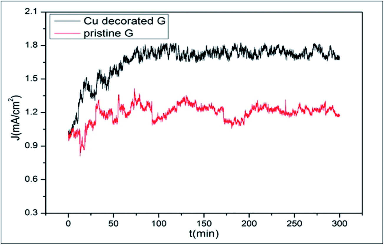 | ||
| Fig. 7 Emission stabilities of pristine graphene and Cu-decorated graphene with a decoration time of 4.5 min. Reproduced with permission.96 © 2016 Elsevier. | ||
3.2 Modulation via hydrogenation of graphene
Decoration of graphene with hydrogen is a widely used covalent functionalization method. Graphene is transformed to “graphane”, a fully hydrogenated form of graphene with a formula unit of (CH)n. Ideally, every carbon atom in the graphene layer forms a covalent bond with a hydrogen atom (H), which results in transformation of the hybridization of the graphene lattice from sp2 to sp3; as a result, the graphene layer becomes buckled.99 Graphane has two conformers, chair and boat. In the chair conformer, the H atoms alternate on both sides of the carbon atom layer, whereas in the boat conformer, the H atoms alternate in pairs. The C–C bond length of the chair conformer (0.152 nm) is greater than the graphene C–C bond length (0.142 nm). Two different C–C bond lengths, 0.152 nm and 0.156 nm, are predicted for the boat conformer. The calculated binding energy for the chair conformer, 6.56 eV per atom, and that of the boat conformer, 6.50 eV per atom, suggest that the chair is the most stable conformer of graphane.Recently, metal-free photo-hydrogenation of graphene was performed at room temperature. The reaction of graphene and formic acid in aqueous solution was carried out in the presence of visible light irradiation, where formic acid was used as the hydrogenation source.100 The hydrogenation capability of graphene was found to be affected by the number of layers of graphene. Raman spectroscopy revealed a higher extent of hydrogen coverage for 2- and 3-layer graphene in comparison to single layer graphene.101 The nature of the metal insulator transition for hydrogenated graphene with increasing percentage of hydrogen coverage was explored by DFT calculations.102 Hydrogenation of the (6√3 × 6√3)R30° reconstruction of SiC(0001), known as buffer layer graphene (BLG), in different temperature ranges revealed the adsorption and covalent bonding of hydrogen to BLG. This increases the C–Si bonding at the interface of the BLG and SiC system, accompanied by high n-type doping and band gap opening compared to pristine BLG. However, after reaching a temperature of 700 °C, H atoms began to intercalate between the BLG and SiC interface; this resulted in the development of quasi-free-standing single layer graphene (QFSG).103 According to DFT, hydrogen atoms can be removed from one side of graphane by an external electric field. This leads to semi-hydrogenated graphene, called graphone, which is an indirect band gap (0.43 eV) ferromagnetic semiconductor. It is predicted that hydrogenation of graphene will tune its metallic and nonmagnetic characteristics to semiconducting and magnetic, respectively.104,105 Recently, a magnetic moment was recorded for the adsorption of hydrogen on graphene. STM and DFT studies revealed the presence of a spin polarized state at the carbon lattice, which is directly opposite to that where hydrogen adsorption occurs. The magnetic moment was found to be controllable via using the STM tip.106 First principle studies of hydrogen adsorbed on the surface of graphene confirmed the band gap opening. It was shown that size of the gap is directly related to the density of adsorbed hydrogen on the graphene surface.107 The DFT band gap is approximately 3.5 eV for local density approximation (LDA) and 4.4 eV with a hybrid functional (HSE06).108 GW studies of graphane confirmed minimum band gaps of 5.4 eV and 4.9 eV for the stable chair conformer (Fig. 8(a)) and the metastable boat conformer (Fig. 8(b)), respectively.109
 | ||
| Fig. 8 (a) and (b) GGA band structure (black solid lines) and GW band structure (red circles) of CH in the chair and boat conformations, respectively. The top of the valence bands is set to zero energy. Reproduced with permission.109 © 2009 American Physical Society. | ||
A band gap of 3.9 eV, close to the DFT calculated value, has been achieved by hydrogenation of CVD-grown single layer graphene using an indirect hydrogen plasma approach. The performance of the prepared material as a FET at room temperature showed the highest current change (103 on/off) ratio. Furthermore, hydrogenated graphene can be transformed to pristine graphene by heating.110 The coverage-dependent band gap opening and ability to convert the charge carrier behaviour from n-type to p-type by surface doping of hydrogenated graphene on the SiO2 substrate reveals its potential applications in p–n junctions.111 Moreover, the p–n junction for graphene-based FETs was successfully obtained by doping graphene through selective exposure to hydrogen.112
Hydrogenated graphene showed good hydrogen adsorption ability due to its nano-size, high stability and comparatively strong graphane–metal atom binding. A DFT study has been conducted to investigate the impact of strain on the hydrogen adsorption capacity of Li-doped graphane. This study revealed hydrogen adsorption capacities of 9.37 wt% (without strain) and 12.12 wt% (with strain).113 The degree of hydrogenation greatly influenced the electrochemical properties of hydrogenated graphene. Hydrogenation of graphene slows the heterogeneous electron transfer (HET) rate and increases the charge transfer resistance.114 Hydrogenated graphene has also shown potential in the electrochemical detection of biomarkers. However, its use was found to be limited in the detection of nitro-aromatic compounds, specifically 2,4,6-trinitrotoluene (TNT), compared to pristine graphene. This detection is limited by the damage caused by hydrogenation into the sp2 structure.115
3.3 Modulation via halogenation of graphene
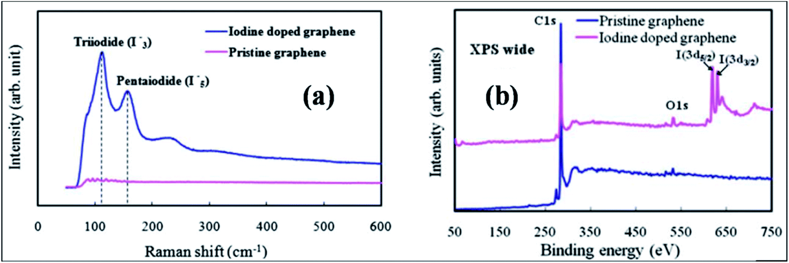 | ||
| Fig. 9 (a) Raman spectral plot displaying the formation of I3− and I5− in the structure of graphene. (b) XPS spectra of pristine and iodine-doped graphene films. Reproduced with permission.117 © 2011 Royal Society of Chemistry. | ||
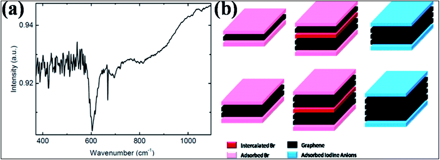 | ||
| Fig. 10 (a) FTIR spectrum for Br-G showing a peak for the Br and G bond at 600 cm−1. Reproduced with permission.118 © 2013 John Wiley and Sons. (b) Schematic of few-layer graphene structure exposed to Br2 (left) and I2 (right) vapors. The left side corresponds to the 3-layer and 4-layer structures both intercalated (dark pink) and adsorbed (light pink) by Br2 layers. The right side represents the 3-layer and 4-layer structures adsorbed (light blue) by iodine anion layers without intercalation. Reproduced with permission.124 © 2009 American Chemical Society. | ||
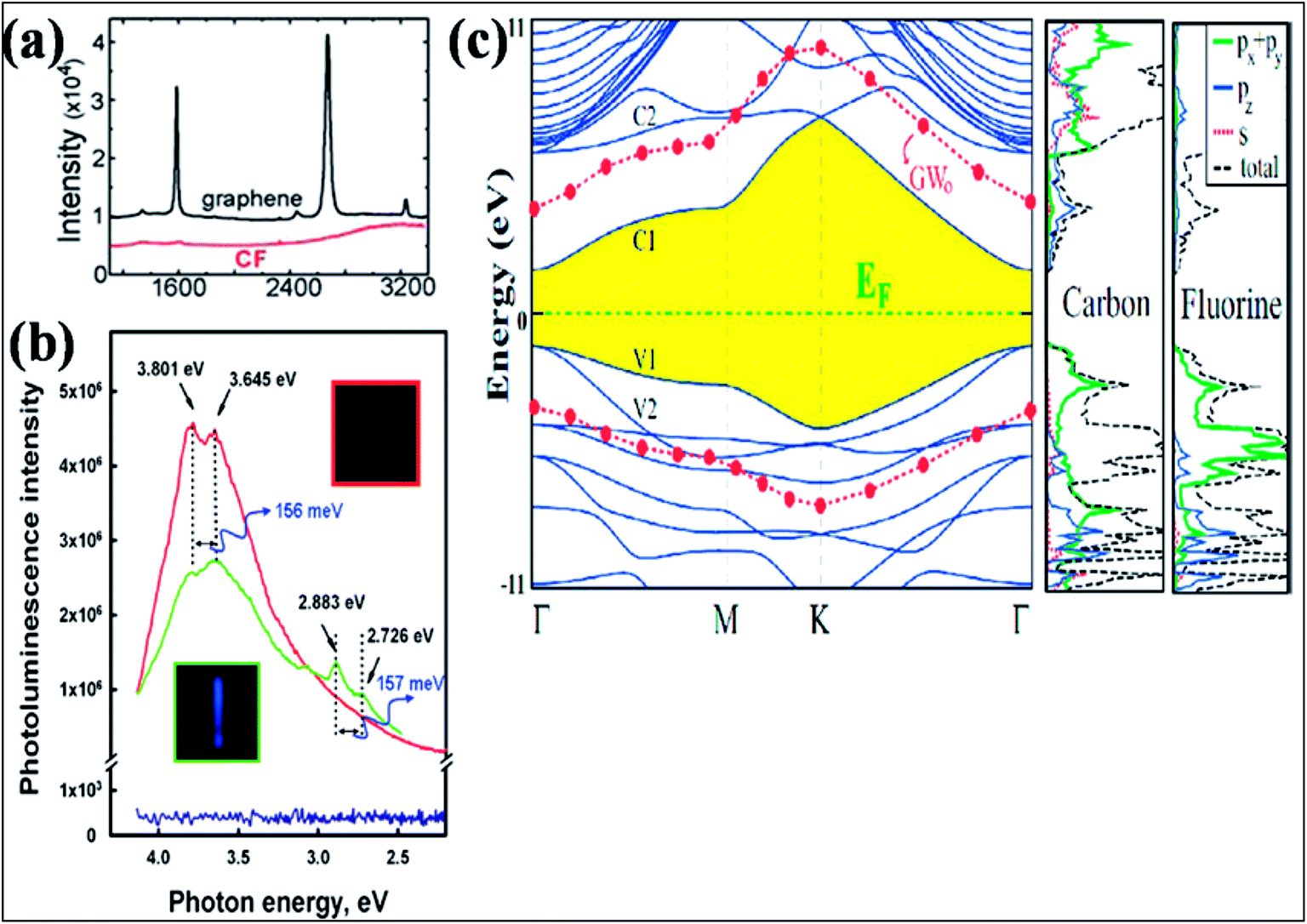 | ||
| Fig. 11 (a) Raman spectra comparing graphene on SiO2 and CF formed on SOI. Reproduced with permission.129 © 2010 American Chemical Society. (b) Room temperature recorded photoluminescence emission (excitation at 290 nm (4.275 eV)) of graphene shown in blue (with no PL peak) and fluorographene (green, fluorination for 1 day; red, fluorination for 5 days). Reproduced with permission from ref. 131. © 2011 American Chemical Society. (c) Band structure and orbital PDOS together with total DOS of fluorographene. The LDA recorded band gap is shaded, and the Fermi level is set to zero energy. After GW0 correction, the conduction and valence band edges are represented by filled (red) circles. Reproduced with permission.132 © 2011 American Physical Society. | ||
Investigation of the DOS of fluorographene by near edge X-ray absorption spectroscopy (NEXAFS) confirmed the transition of the sp2 state of graphene to sp3 due to fluorination.131 Experimental band gaps of 3 eV (ref. 128) and 3.8 eV (ref. 131) were recorded for fluorographene dispersed in acetone. The two photoluminescence (PL) peaks observed at 3.80 eV and 3.65 eV shown in Fig. 11(b) confirm that fluorographene is a wide band gap semiconductor.131 DFT calculations suggest that fluorographene is a direct band gap material, as shown in Fig. 11(c).132 The predicted band gap value of about 3.2 eV from GGA-DFT suggests insulating behavior of fluorographene.133 The HSE06 functional suggested a band gap of 5.1 eV for CF.108 The band gap (7.0 to 8.3 eV) predicted by the high level GW approximation method is approximately two times larger than the value provided by GGA-DFT.134,135 At room temperature, fluorographene showed an electrical resistance of 10 GΩ and a large band gap due to its highly insulating behavior.127 It is elucidated that partially fluorinated graphene at 25% coverage has 6-fold higher resistance than pristine graphene due to the presence of fluorine atoms.129 The fabrication of a transistor has been demonstrated using monolayer fluorinated graphene. Due to fluorination, enhancement of the resistance in the electroneutrality region has been observed, which suggests a mobility gap.130 Furthermore, fluorographene showed a rapid decrease in band gap on applying large strain; however, small strain did not change the band gap.136 Due to the presence of edge states and defects at temperatures below 50 K, weak paramagnetism was observed in diamagnetic graphene.137
Moreover, fluorination of graphene significantly changes its magnetic properties due to the formation of C–F bonds. Double-sided uneven partially fluorinated graphene with wrinkle and ripple structures has shown non-magnetic and magnetic behavior, respectively.138 Moreover, the application of tensile strain resulted in a notable increase in the induced magnetic moment.138 Due to its paramagnetic behavior137 and intriguing C–F bonds,139 fluorographene is an attractive material for biological sciences. The successful uses of fluorinated GO as a magnetic resonance imaging (MRI) (without magnetic nano-particles) and photo acoustic contrast agent have been reported.140 Moreover, the potential of this material has been explored for ultrasound imaging and therapeutic applications.140,141 The high tribological performance of graphene has been found to be further enhanced by fluorinating its structure. This enhancement is attributed to the C–F bonding structure.142 Interestingly, due to its low coefficient of friction and high durability, fluorinated graphene may be used in ultrathin solid lubricants and anti-wear composites. Electrochemical properties tests of fluorographite showed that the speed of HET can be increased by increasing the C/F ratio.143 Fluorographene and fluorinated graphene have become materials of interest for energy conversion storage devices144,145 and amphiphobicity.146
![[thin space (1/6-em)]](https://www.rsc.org/images/entities/char_2009.gif) :Cl ratio can be tuned by controlling the dc bias plasma reaction time for chlorination.148 The adsorption mechanism of a single Cl adatom on the surface of graphene is observed to be different than those of H and F adsorption.149 Maximum coverage of 25% with a homogenous pattern of Cl atoms was reported for chlorination of both sides of graphene.149 DFT calculations endorsed the facile attachment of chlorine to the edges of graphene compared to its adsorption onto the basal plane.150
:Cl ratio can be tuned by controlling the dc bias plasma reaction time for chlorination.148 The adsorption mechanism of a single Cl adatom on the surface of graphene is observed to be different than those of H and F adsorption.149 Maximum coverage of 25% with a homogenous pattern of Cl atoms was reported for chlorination of both sides of graphene.149 DFT calculations endorsed the facile attachment of chlorine to the edges of graphene compared to its adsorption onto the basal plane.150The synthesis of CCl by one-step plasma enhanced chemical vapor deposition is schematically represented in Fig. 12(a). XPS confirmed CuCl2 on Cu foils as the agent of chlorination. XPS and Raman spectra data analysis indicated C–Cl covalent bond formation for chlorinated graphene (Fig. 12(b) and (c), respectively).151 Chlorination of graphene has been demonstrated by p-type doping.150,151 Partial chlorination of graphene via UV-light irradiation in a liquid chlorine medium with chlorine coverage of 30 atoms has also been reported. However, laser irradiation of a chlorographene sample leads to dechlorination.120 The chlorination of graphene for coverage on one side as well as both sides revealed that two-sided chlorinated graphene is stable and shows a direct band semiconducting structure at T = 0 K as well as at room temperature; the non-bonding chair conformer was found to be the unstable structure.136 Chlorination via a photochemical process transformed the sp2 hybridized character of graphene to sp3-hybridization. It also altered the zero gap nature of graphene to an insulator. The reported coverage of chlorine atoms is about 8%. In addition, all the used characterization techniques explored the non-destructive and homogenous nature of photochlorination.147 However, the process of chlorination by adsorption of chlorine on both sides of graphene for various coverages and different configuration sites revealed tuning of the band gap of graphene.119,149 The GGA-DFT calculated band gap is 1.4 eV,134 which shows semiconducting wide band gap or insulating behavior. As GGA underestimates the band gap, a more authentic value of 2.81 eV was obtained for the band gap of chlorographene using the hybrid HSE06 functional.134 A band gap of 4.93 eV was reported for the highest level of GW-HSE06, which also includes electron–electron interactions. CCl is predicted to be a direct band gap material. The maximum band gap is observed at the K point (Fig. 13).134 Electrochemical properties tests of halogens showed a faster HET rate for Cl compared to Br and iodine; this is due to the high electronegativity (3.16) of chlorine.118
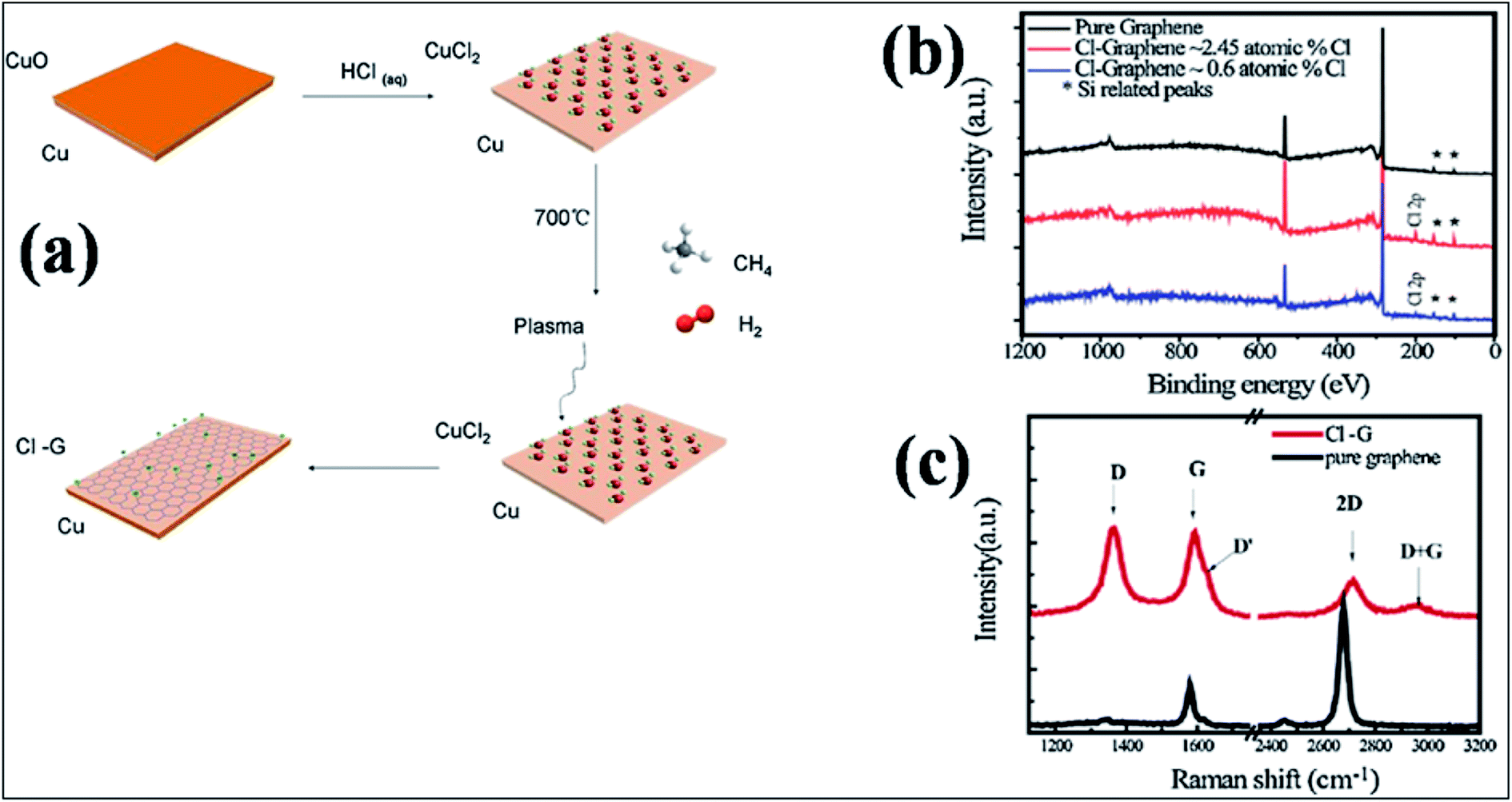 | ||
| Fig. 12 (a) Schematic representation of the one-step synthesis of chlorinated mono-layer graphene: (b) XPS plots of CCl on SiO2 compared with that of pure graphene. (c) Raman spectra of graphene (black lines) and CCl (red lines) grown on SiO2 substrate. Reproduced with permission.151 © 2015 Elsevier. | ||
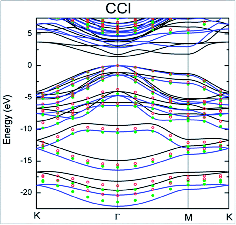 | ||
| Fig. 13 The electronic band structure of CCl. Reproduced with permission.134 © 2013 American Chemical Society. | ||
3.4 Concluding remarks and future outlook
The second method, which is considered in the present study for the modulation of the electronic properties and magnetism of graphene, is surface doping via adsorption of metals and non-metal atoms on the graphene surface. Adsorption of these adatoms induces lattice distortion, an electric dipole moment and a spin polarized magnetic moment, which affects the morphological growth of metals on graphene. The phenomena of distortion, band gap opening and the magnetic dipole moment in graphene are different for different adsorbed atoms. Alkali and alkaline earth metals lead to n-type doping of graphene due to their ability to easily evolve electrons when adsorbed on the surface of graphene. Group (I–III) adatoms show ionic bonding and minimal change to the electronic structure of graphene. However, group IV elements, d-valence electrons, transition metals and noble metal atoms establish covalent bonds with the graphene surface. This covalent bond formation perturbs the inherent hybridization of graphene. The strong hybridization between adatoms and the π and π* orbitals of graphene and charge transfer from the adatom orbitals to graphene tune the electronic structure of graphene. The transfer of charge between the different orbitals of metal adatoms and graphene also induces an electric dipole moment, spin-polarization and a magnetic moment in graphene. The adsorption mechanisms, magnetism and band gap opening of graphene by many metal atoms have already been studied. However, many challenges related to the adsorption of metals and non-metals on the surface of graphene, particularly Ca, Ba and Sr adsorption, for modulation of the band gap and magnetism of graphene remain to be addressed by experimentalists.Covalent functionalization methods of graphene, such as hydrogenation and halogenation, are powerful tools to engineer the band gap and induce magnetism in the graphene lattice. Ab initio DFT calculations showed the transformation of graphene to a metal and then to an insulator with increasing percentage of hydrogen coverage. STM and DFT studies revealed the presence of the spin polarized state and a tunable magnetic moment for hydrogen-adsorbed graphene. The degree of hydrogenation greatly influences the electrochemical properties of hydrogenated graphene. Hydrogenation of graphene slows the heterogeneous electron transfer rate and increases the speed of charge transfer resistance. Incompletely hydrogenated graphene exhibits ferromagnetism. Numerous experimental techniques have been developed for the synthesis of fully hydrogenated graphene. However, further improvements in the cost, efficiency and environmental suitability of hydrogenation techniques towards the fabrication of graphane are currently necessary. Because iodine has the lowest electronegativity (2.6) in the halogen family, I-doped graphene shows the lowest HET process. Halogenated graphene exhibits good electrochemical performance towards the ORR. Due to its wide band gap, paramagnetic behavior and intriguing C–F bonds, fluorographene is an attractive material in the fields of electronics, biological sciences, energy conversion, energy storage devices and amphiphobicity. The establishment of novel and efficient methodologies to manipulate the magnetic properties of graphene without disrupting its intrinsic properties, such as high charge conductivity, remains to be accomplished. Although the field of halogenation of graphene has rapidly developed, there are still some unclear phenomena and discrepancies related to the unclear C–F bonding nature, actual band gaps and uniform commercial scale production of fluorographene and chlorographene. These discrepancies represent new challenges to both experimentalists and theoreticians.
4. Modulation via substitution and their applications
Substitutional doping into the carbon lattice with electron-withdrawing or -donating heteroatoms enables tailoring of the structural, electronic, magnetic and electrochemical properties of graphene. Many novel and improved properties are developed via substitutional doping of graphene; these vary with the type, concentration and size of the dopant. Substitutional doping of graphene is an efficient and widely used method to tailor the electronic and magnetic properties of graphene. These newly developed materials have demonstrated superior potential for practical applications.4.1 Substitution of group IIIA elements in graphene
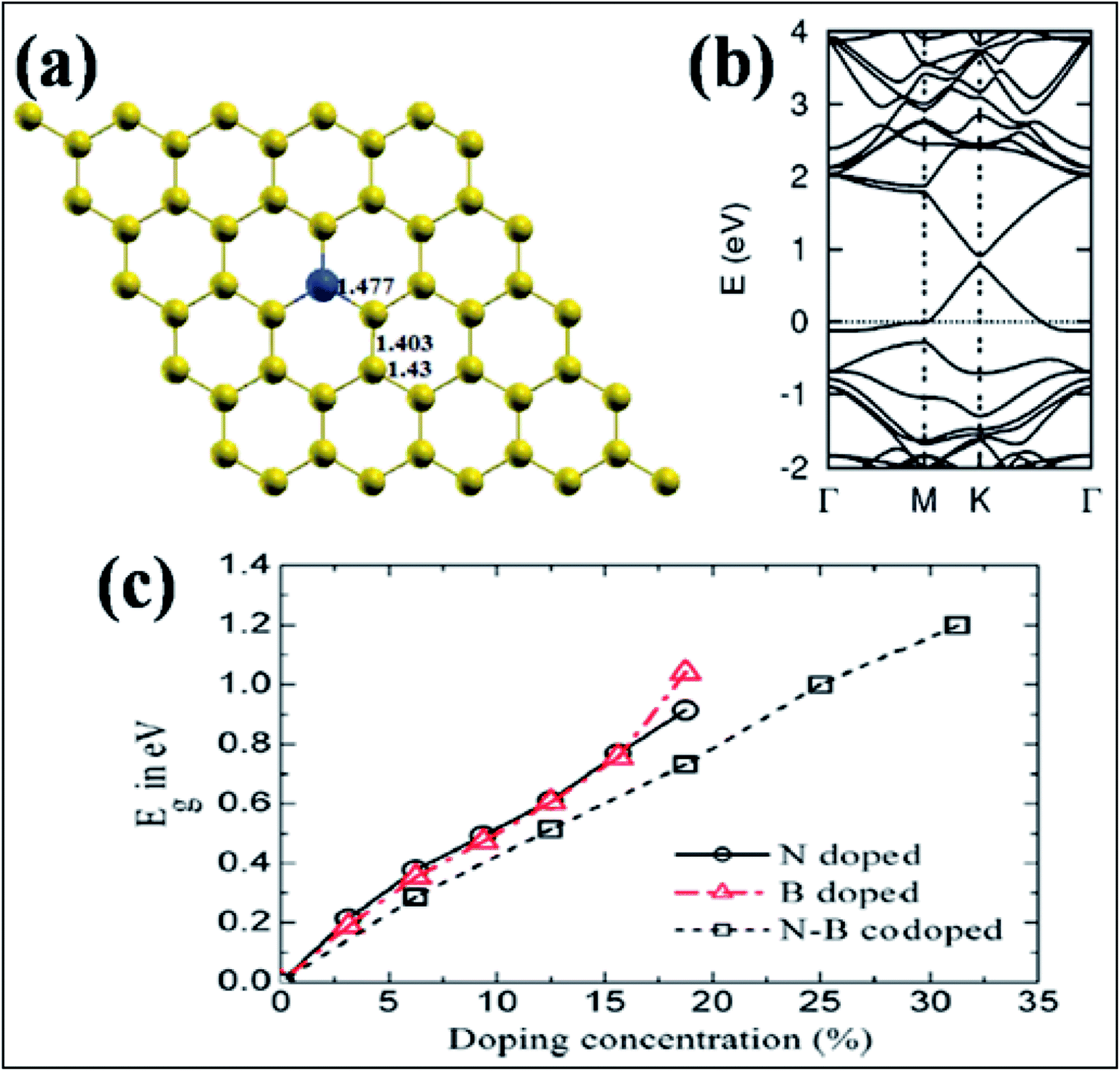
Among the elements of group IIIA, extensive studies have been conducted on substitutional doping of boron in graphene due to its similar atomic size to the C atoms of graphene. Different techniques, such as the arc discharge method,152 CVD,153,154 hydro and solvothermal treatments,155,156 Wurtz-type reductive coupling157 and post functionalization158 with different graphene and boron sources have been adopted by many groups for the synthesis of boron-substituted graphene (B-G). The substituted B atom does not change the hexagonal sp2 planar characteristics of graphene. However, the B–C ≈ 1.50 Å bond is found to be larger than the C–C bond of pristine graphene, which leads to alteration of the lattice parameters.159,160Boron substitution in graphene has been found to be an efficient tool to alter the electronic structure and zero band gap of graphene.152,159,160 The linear dispersion of the electronic bands of graphene within 1 eV of its Fermi energy is almost unaltered via B- and N substitution. At a substitution rate of 2%, B in graphene has been shown to shift the Fermi level by −0.65 eV. This is attributed to electronic effects via the dopant (96%) and strain (4%) caused by relaxation of the doped structure.152 The pz orbital of B is empty due to the presence of only three valence electrons. The unpaired single pz electron on the neighboring C atom always results in local spin density.161 In B-G (Fig. 14(a)), the high electronegativity of C compared to B downshifts the Fermi level of graphene, which is depicted in Fig. 14(b).159 B-G is found to exhibit p-type doped characteristics154,159 with an electron mobility of 800 cm2 V−1 s−1 or about 350 to 550 cm2 V−1 s−1 as calculated by electric transport measurements and back-gate FETs, respectively.153,154 B-Doped graphene on a polycrystalline copper surface has demonstrated neutral doping.162 The reason for this neutrality is the combination of n-type doping caused by metal–graphene interactions, with p-type doping induced by the B-dopant.162
 | ||
| Fig. 14 (a) Substitution of B (blue ball) in graphene. (b) Band structure of a single B-substituted graphene sheet. Reproduced with permission.159 © 2013 Royal Society of Chemistry. (c) Variation of Eg with N, B, and N–B pair doping concentrations. Reproduced with permission.164 © 2014 Elsevier. | ||
Band gap opening in graphene via B substitution was found to be sensitive to dopant concentration159,163,164 and the number of graphene layers163 while also being found to be insensitive to the dopant type (N and B).164 The variation of band gap energy (Eg) with respect to the doping concentrations of different dopants is depicted in Fig. 14(c).164 Semimetallic graphene was transformed to a semiconductor via substitution of B and Al.159,165 For both B and Al-substituted graphene, the respective reported band gaps are 0.14 eV and 0.11/0.16 eV for spin up/spin down.159 Tight binding and DFT calculations have shown that band gap opening of graphene through B-substitution is also sensitive to the arrangement of B with respect to the superlattice symmetry. For the arrangements of B-dopant according to D3h and D6h symmetry, band gap opening and preservation of the Dirac cones have been observed, respectively.166
Theoretical investigation of the transport properties of doped graphene reported that at high concentrations (4.0%) of B or N doping, the doped graphene retained the excellent transport properties of pure graphene. However, the observed mobilities of electrons and holes were found to be non-symmetric with respect to the Dirac point,167 which is in agreement with experimental results for B-G.153 The concentrations of B and N dopants influence the DOS, Fermi energy and electrical conductivity of graphene. High dopant concentrations at lower temperature increased the electrical conductivity, while the opposite effect was found in the high temperature region.168 Non-spin polarized behavior has been reported for B-G.169 However, a dopant concentration-dependent spin polarized nature was observed for B-G.170 Weak magnetism is suggested by theoretical calculations on the B-G system. Moreover, magnetism at the graphene zigzag edges was also found to be weakened by the presence of B-clusters.171 A magnetic moment of 1 μB is reported for Al-substituted graphene.165 Induced local spin density at the basal plane of graphene via B-substitution promotes the adsorption of oxygen and OOH molecules on graphene, which also enhances its catalytic performance towards the ORR.161
B-G is a novel emerging material for electrochemical energy storage devices due to its excellent performance. B-Substituted materials are playing a considerable role in the development of supercapacitor technology. Different techniques and strategies used for the fabrication of supercapacitors based on B-G systems revealed high capacitance and cyclic stability compared to pristine graphene. Boron-doped thermally reduced graphene oxide (BT-rGO), synthesized via annealing a mixture of freeze-dried GO and B2O3, demonstrated higher specific capacitance (448 F g−1), as shown in Fig. 15(b), and better cyclic stability, as shown in Fig. 15(c) and (d), compared to undoped thermally reduced graphene oxide (T-rGO). This high capacitance was predicted to be due to the other side redox reaction. This high capacitance reveals the potential use of this material in electrochemical double layered capacitors (Fig. 15(a)).172 B-G synthesis by pyrolysis of GO and boric acid exhibited a capacitance of 172.5 F g−1 at 0.5 A g−1, excellent cycling stability (96.5% retained after 5000 cycles) and improved capacitance by approximately 80% compared to pristine graphene. All these enhancements are attributed to the formation of functional groups during B-doping in graphene.173 At a high specific capacitance of 318 F g−1 in 6.0 M KOH solution, improved cyclic performance was reported for a supercapacitor based on a hybrid structure of polyaniline and B-G.174 Recently, boron-doped reduced graphene oxide (B-rGO), obtained by dielectric barrier discharge (DBD) plasma treatment of GO and boric acid, was explored for its potential application in supercapacitor electrodes. The obtained material showed remarkable capacitance accompanied by high electrochemical stability.175 A flexible micro supercapacitor obtained via a commercial laser writing technique showed a capacitance of 16.5 mF cm−2, which is 3 times higher than those of undoped devices. Furthermore, the obtained volumetric energy density was 5 to 10 times larger than that of the undoped material. All reported supercapacitor performance of the prepared material was retained even after mechanical deformation and extended cycles.176
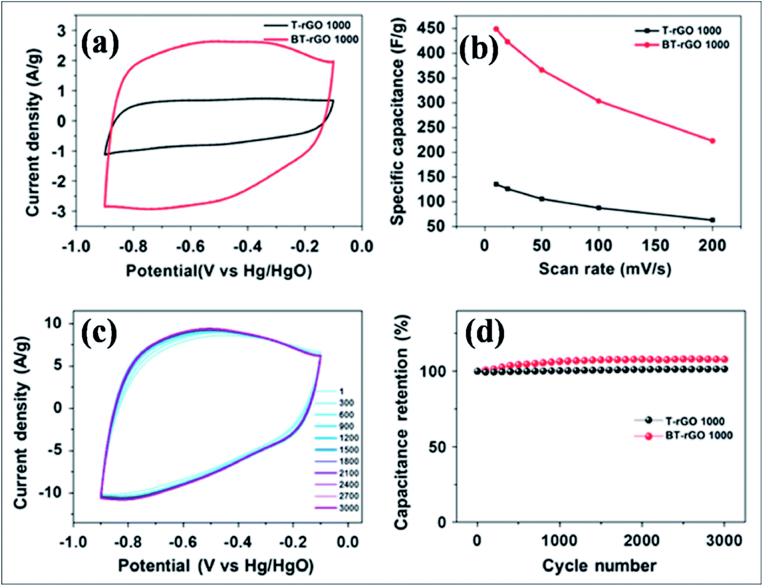 | ||
| Fig. 15 (a) Cyclic voltammetry (CV) curves for T-rGO and BT-rGO at a scan rate of 10 mV s−1, (b) specific capacitances as a function of scan rate, (c) CV curves for 3000 cycles at a scan rate of 50 mV s−1, and (d) retained capacitance as a function of cycle number of T-rGO and BT-rGO electrodes. Reproduced with permission.172 © 2015 Nature Publishing Group. | ||
In addition to B-G-based supercapacitors, extended experimental and theoretical calculations were conducted to investigate the potential of B-G in Li177,178 and Na ion batteries.179 A lithium ion battery (LIB) anode based on B-G showed a higher capacitance of 1549 mA h g−1 at a 50 mA g−1 charge/discharge rate (Fig. 16(a)), which is far better than the capacitance of 1043 mA h g−1 obtained by the system based on the same amount of N-G. This capacity was found to be preserved even at a superfast charge/discharge rate (235 mA h g−1 at 25 A g−1). After 30 cycles, B-dopants increased the retained reversible capacity of isolated graphene from 66.8% to 79.2% (Fig. 16(b)). The excellent performance of this system is attributed to the characteristics of the 2D material, disorder and defects created by B-dopants, an increase in the interlayer distance, and the electrical conductivity, electrode/electrolyte wettability and thermal stability of the dopants. All of these characteristics provide a good platform for the intercalation and diffusion of Li ions.156 Through first principles calculations, enhancement of Li storage is observed in B-G.180,181 Li ions have a tendency to form clusters on the surface of pristine graphene, which significantly affects the Li absorption capacity of graphene.180 B-dopant controls the clustering of Li180 and confers electron deficiency on the graphene system; thus, more Li ions gather on its surface than on that of pristine graphene.181 Moreover, B-G has been proven to have good potential applications in different sectors, such as sensors,182 biomedicine183 and photovoltaics.65
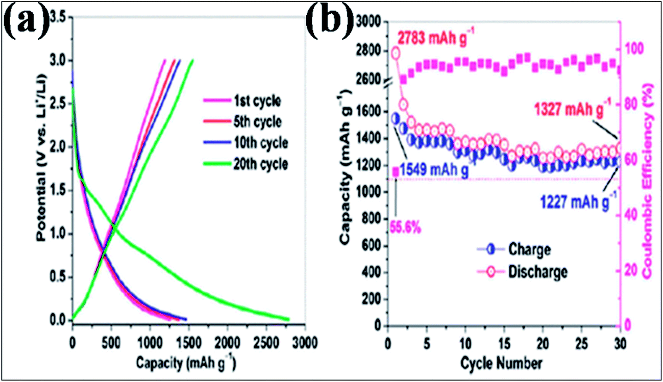 | ||
| Fig. 16 (a) Galvanostatic plots for the charge/discharge cycle performance and (b) coulombic efficiency of the B-G electrode at a low current rate of 50 mA g−1 between 3.0 and 0.01 V versus Li+/Li. Reproduced with permission.156 © 2011 American Chemical Society. | ||
4.2 Substitution of group IVA elements in graphene
Silicon, a 3p element and a member of group IVA, is a widely substituted element in graphene. Epitaxially grown graphene via thermal decomposition of SiC is thought to be intrinsically Si-doped.184 Controllable synthesis of large area Si-G has been achieved by reaction of methoxytrimethylsilane (C4H12OSi) and hexane.185 The creation of a curvature around the Si substitution site facilitates interaction between dye molecules and the graphene sheet. The synthesis of silicene, a two-dimensional allotrope of Si that consists of a honeycomb structure with a weakly buckled geometry, suggests a method for the production of graphene-silicone 2D compounds.186 The Si atoms substituted in graphene (Si-G) can be seen using annular dark-field (ADF) and STM imaging tools. The obtained images are depicted in Fig. 17(a–f).187 The Si-atoms were found to be stable in the graphene structure, which is also supported by DFT studies. 187 The threefold coordinated Si atom in graphene was found to adopt sp3-hybridization.187 The presence of Si substitutional impurities in graphene was found to influence the planar structural, electronic and transport properties of graphene.187 A band gap of 2.13 eV was observed for Si substitution, while germanium (Ge) and tin (Sn) doping reduced this band gap for equal doping concentrations.188 Band gap tuning of graphene and semiconducting behavior has been observed for Si-substitution.189,190 The band gap is found to be influenced by the number of atoms of Si. The band gap increases with increasing number of dopant atoms (silicon atoms) present in the unit cell. For a 50% proportion of Si, the band gaps calculated by DFT and GW levels are 2.65 eV and 2.78 eV, respectively.190 Si-G used in a gallium arsenide (GaAs) solar cell showed 33.7% more power conversion efficiency than solar cells containing only graphene/GaAs.191 Moreover, the gas absorbing ability of Si-G provides possibilities to explore the potential applications of this material in gas sensors.187,192 | ||
| Fig. 17 (a–c) STEM-ADF images of graphene substituted by Si atoms in common defect configurations with threefold or fourfold coordination in monolayer graphene. (d–f) Schematics of the obtained images of (a–c), respectively. The chemical identity of each atom was obtained from quantitative ADF image analysis. Reproduced with permission.187 © 2012 American Physical Society. | ||
4.3 Substitution of group VA elements in graphene
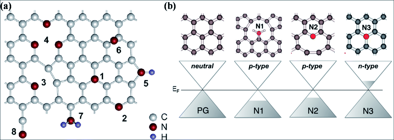
Nitrogen substitution is an efficient approach to modify the intrinsic properties of graphene. Nitrogen substitution influences the surface chemistry and alters the electronic, magnetic and electrochemical properties of graphene, accompanied by local changes in the elemental composition of graphene. Different technical approaches using different N-precursors have been used for N substitution, including CVD direct synthesis,193,194 arc discharge,152,195 solvothermal techniques,196 segregation direct synthesis,197 post-synthesis thermal treatment,198 hydrazine hydrate treatment199 and nitrogen plasma treatment.200,201 N-Substituted graphene (N-G) produced by the exfoliation of graphite in the presence of N-atmosphere is an efficient source for lowering the reactivity of defects and C–C reconstruction at defect sites.202The different feasible bonding configurations of N dopants in graphene are shown in Fig. 18(a). Among these, the three main types are graphitic or quaternary N, pyridinic N and pyrrolic N. Pyridinic N and graphitic N are sp2 hybridized structures, while pyrrolic N is sp3 hybridized. Graphitic N refers to the nitrogen atoms, which are assimilated into graphene layers by substituting C-atoms within the hexagon. Pyridinic N atoms are those that are present at the defect sites or edges of graphene. Pyrrolic N atoms, due to their higher binding energy, bond to two carbon atoms and assimilate into five-membered heterocyclic rings.203 The charge transfer per substituted N atom is larger for graphitic N than for pyridinic and pyrrolic nitrogen in graphene.204 For graphitic N or direct substitution, out of five available valence electrons, three electrons of nitrogen connect via three σ-bonds to the adjacent carbon atoms, the fourth electron forms a π bond, and the fifth electron partially participates in the π*-state of the conduction band.205 Theoretical calculations of N-G for the pyridinic and pyrrolic configurations show p-type doping due to their ability to withdraw electrons from graphene.204 However, n-type doping of graphitic N-graphene is due to its electron accepting ability.205 These doping behaviors are shown in Fig. 18(b). Hydrogenation of pyridinic and pyrrolic N is found to transform their doping type from p- to n-type.205
 | ||
| Fig. 18 (a) Possible configurations of N atoms in graphene: 1 – graphitic N, 2 – pyridinic N, 3 – single N pyridinic vacancy, 4 – triple N pyridinic vacancy, 5 – pyrrolic N, 6 – interstitial N or adatom, 7 – amine, 8 – nitrile. Reproduced with permission.203 © 2011 American Chemical Society. (b) Computational representation of the doping effects induced by different bonding types of N dopant compared to pristine graphene. Reproduced with permission.205 © 2012 American Chemical Society. | ||
N substitution induces polarization in the graphene structure because N atoms are more electronegative than C atoms. Charge polarization has been found to affect the electronic and magnetic properties of graphene.206 Upon N-substitution, graphene adopts semiconducting properties and its zero band gap opens.207 The band gap opening, induction of spin polarization and magnetic effects in graphene are sensitive to the doping concentration and doping configuration of nitrogen.170,208 However, the spin polarization and magnetic moment of N-G also depend on the presence of non-bonding electrons. Graphitic-N has no non-bonding electrons; thus, spin polarization and a magnetic moment are not observed. On the other hand, in both the pyrrolic and pyridine structures, non-bonding electrons are available. However, a strong magnetic moment is shown in pyrrolic N due to the formation of π and π*, while pyridinic N shows only a weak magnetic moment.209 Recently, N-G produced via self-propagating high-temperature synthesis (SHS) showed ferromagnetic properties at a high Curie temperature.210 Some studies of edge doping of graphene via N atoms have also reported spin polarization and magnetic moments in graphene.211 Doped graphene nanoribbon edges showed different ranges of magnetic moment depending on the N-doping sites; moreover, N-doped graphene nanoribbons with translational grain boundaries revealed spin-polarized ferromagnetic ordering.211
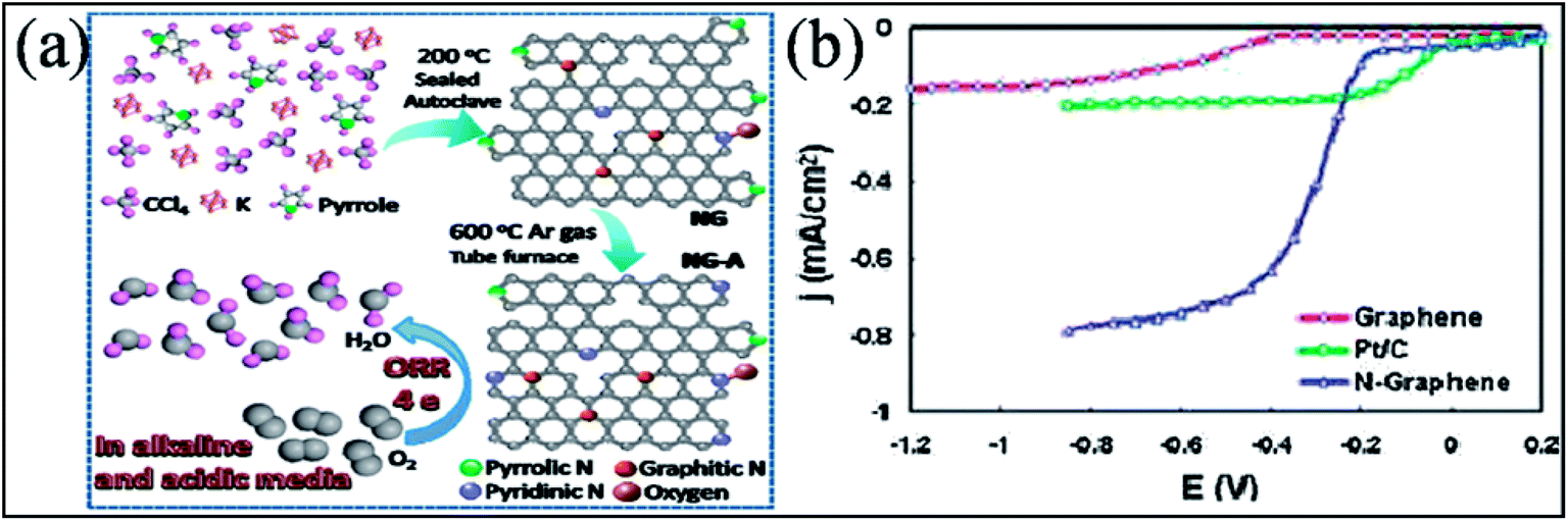
Many experimental193,194,212,213 and theoretical efforts214 have been devoted to studying the catalytic performance of N-G, all of which resulted in enhancement of the efficiency of the catalytic activity of N-G towards the ORR in fuel cells. These enhanced properties are found to be sensitive to nitrogen graphene configuration types and nitrogen content. Different investigations resulted in different conclusions because of the presence of more than one type of nitrogen in N-G.193,198 A N-G material prepared by a solvothermal technique accompanied by thermal annealing (represented as NG-A) showed evolution of its configuration from pyrrolic-N to pyridinic-N. This material displayed better catalytic activity in both acidic and alkaline media. A schematic of the as-prepared material is shown in Fig. 19(a).213 In contrast to the two-step and two-electron ORR catalytic pathway of pristine graphene, N-G catalysts, which contain more than one N-type, follow a one-step and four-electron pathway.194 However, a two-electron pathway is observed in the case of N-G with a pyridinic N configuration.198 At large potential ranges, N-G exhibits a constant catalytic current density approximately 3 times higher than that of a commercial platinum/carbon (Pt/C) electrode, as shown in Fig. 19(b).194 Furthermore, a decrease in the catalytic activity of the pyridinic N configuration is observed when the atomic percentage of nitrogen is increased.193 Similarly, for large N-content in N-G, theoretical calculation suggests oxygen poisoning. N-G exhibits greater stability, high tolerance to crossover effects and high selectivity; moreover, its activity is not influenced by addition of CO or methanol.215 The power density and catalytic performance of a direct methanol fuel cell (DMFC) anode fabricated using a N-G–CNT hybrid with well-distributed PtRu is higher than those of standard commercial PtRu/CNT catalysts.216 On the other hand, Li storage capacity is significantly enhanced by N-substitution in graphene because it induces more defects and provides favorable binding sites for Li ions.217 The performance of LIBs218 and lithium oxygen batteries (LiO)219 are found to be enhanced by N-substitution in graphene. This method also offers higher reversible discharge capacity and longer cyclic stability compared to pristine graphene. However, due to the different types of N-G configuration, it has been shown that perpendicular diffusion of Li ions in graphene sheets is enhanced in the cases of pyridinic and pyrrolic N but not in the case of N-graphene.220 This enhancement can be attributed to the theoretically observed higher binding energy of Li ion to the two former configurations compared to the latter.221 Moreover, the performance of electrochemical sensors has been found to increase on using N-G,222 which is attributed to the better electron transfer efficiency of N-G compared to that of pristine graphene.222
 | ||
| Fig. 19 (a) Schematic of the synthesis process of N-G and the ORR catalyzed by N-G. Reproduced with permission.213 © 2016 Springer. (b) Rotating ring disk electrode (RRDE) voltammograms for comparison of the ORR in air-saturated 0.1 M KOH for pristine graphene (red line), Pt/C (green line), and N-G (blue line) electrodes. Reproduced with permission.194 © 2010 American Chemical Society. | ||
Due to the enormous applications of electrochemical supercapacitors in a variety of fields, such as electronics, electric vehicles, aircrafts and energy supply devices, much attention is being devoted to N-G based supercapacitors in order to explore their potential to obtain high capacitance, fast charging, long charge discharge cycling stability, etc.223 N-G prepared by hydrothermal reaction of GO and urea showed good specific capacitance (326 F g−1, 0.2 A g−1) in aqueous electrolyte (6 M KOH), accompanied by excellent cycling stability and a columbic efficiency of 99.58%.223 The N-G specific capacitance increased with the N-content.193 Furthermore, the type of N-G configuration also influences the capacitance. The presence of graphitic-N enhanced the conductivity of the graphene materials, while pyrrolic and pyridinic-N are important for the enhancement of psuedocapacitance.223 Nitrogen-doped crumpled graphene sheets224 obtained via thermal expansion showed a specific capacitance of 270 F g−1 at a discharge current density of 1 A g−1. Moreover, at this density rate, 97% of the capacitance was retained even after 2000 cycles.224 Furthermore, N-G has been proven to exhibit good gas absorption225 and field emission226 properties.
Elemental phosphorus, as a member of the same group as N, contains the same number of valence electrons and shows the same chemical properties. Substitution of P in graphene changes the sp2 hybridized structure of pure graphene to sp3. P substitution creates more structural distortion in the graphene lattice compared to N-substitution. P-Substituted graphene (P-G) after bonding with three C atoms of graphene presents a pyramid-like structure in which the C–P bond length is greater than the C–C bond length in the pristine graphene structure.227 Phosphorous provides more orbitals in the P-G hybrid structure compared to N. Moreover, the C–P bond polarity is found to be opposite to that of the C–N bond because P is more electronegative than both C and N and hence shows more electron donating capability.228 Phosphorous substitution in graphene tailors its electronic structure and magnetic properties.227,229 Theoretical calculations suggested that P substitution in graphene has a low formation energy and introduces a band gap of 0.3 to 0.4 eV. The band gap opening was found to be dependent on the P-concentration.229 Theoretically, n-type doping of graphene with a charge transfer of 0.21 e has been reported for P-G.227 An air stable phosphorus-doped bilayer graphene-based FET showed n-type doping with greater electron mobility than pure bilayer graphene. Moreover, this n-type doping was retained in oxygen atmosphere.231 The calculated magnetic moment of P-G is 1.05 μB.230 P-G synthesized using a process of thermal annealing in the presence of graphite oxide and triphenylphosphine (as C and P sources, respectively) has been proven to demonstrate excellent ORR activity, stability and selectivity. Moreover, this material exhibited good electrochemical properties when used as an anode material in LIBs.232 It has been shown that P-G obtained by pyrolysis of alginate and H2PO4 in the absence of oxygen acts as a good photocatalyst for hydrogen generation from water and methanol mixtures. The catalytic activity was reported to be enhanced by increasing the amount of HPO42−.233 P-G fabricated at high temperatures in the presence of GO and triphenylphosphine showed outstanding room temperature sensing capability of NH3 compared to rGO.234
4.4 Substitution of group VIA elements in graphene
The possible bonding configurations of sulfur (S) with graphene C atoms are C–S–C, C–SOx–C and C–SH, as shown in Fig. 20(a).235 S-Substituted graphene (S-G) has been prepared by utilizing different experimental techniques.236,237 Two compounds, hydrogen sulfide237,238 and benzyl disulfide,235 are widely used S-sources for the preparation of S-G. Thermal exfoliation of graphite oxide in the presence of a sulfur source238,239 and CVD in the presence of liquid precursors238 are used for the preparation of S-G. p-type doping and lower conductivity have been confirmed for S-G based transistors in comparison to undoped pristine graphene.240 Sulfur doping in graphene can also alter the planar structure and tune the electronic properties of graphene.240,241 A theoretical study has shown that S-G can act either as a metallic or a small band gap semiconductor depending on the concentration of S atoms.241 Experiments accompanied by theoretical calculations confirmed ferromagnetism below a temperature of 62 K in sulfur (4.2%)-substituted graphene. This phenomenon was attributed to the substitution and concentration of S-dopants.242 However, in a separate study, quenching of the previously developed local magnetic moment induced by vacancies was observed via S substitutional doping of graphene, which led to diamagnetic, weak ferromagnetic and antiferromagnetic states in graphene.243 The S-G system maintains good electrocatalytic activity for the oxygen reduction reaction.235 S-G prepared via acid exposure of graphene has been proven to be an excellent solid catalyst.236 SEM and quantitative energy dispersive X-ray spectroscopy (EDS) images of S-G are shown in Fig. 20(b–e). The EDS images reveal homogenous distribution of S atoms on the surface of graphene (Fig. 20(e)). Furthermore, this system showed highly water tolerant catalytic activity for the hydrolysis of ethyl acetate.236 The good electrocatalytic activity of S-G via electrochemical methods revealed its potential to replace Pt-based catalysts in fuel cells.244 S-G, prepared via a magnesiothermic reduction technique to transform greenhouse gas CO2 using Na2SO4 as an inorganic S-precursor, exhibited good electrocatalytic activity towards the ORR and excellent durability; it followed a four-electron reaction pathway.245 Furthermore, higher current density246 and remarkable hydrogen uptake capabilities247 were reported for S-G compared to undoped graphene derived from lithium-sulfur batteries.246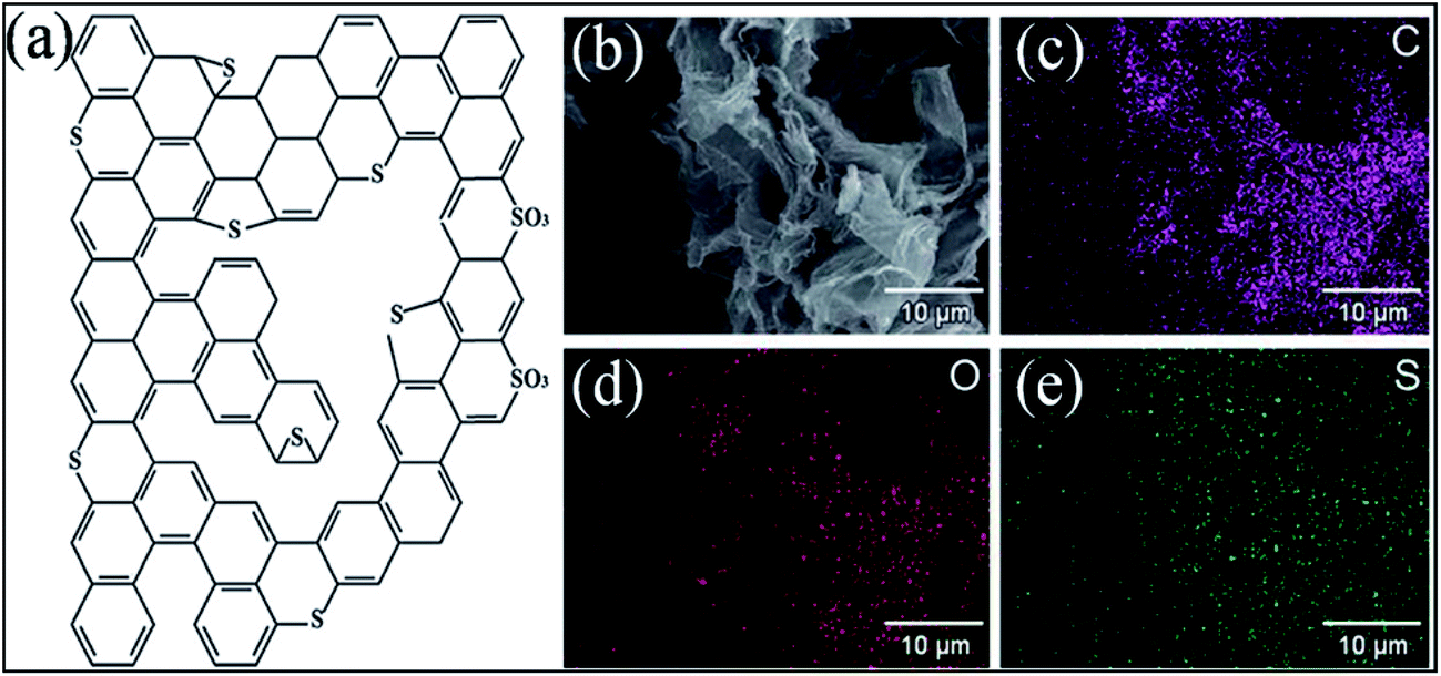 | ||
| Fig. 20 (a) Typical configuration of S-doped graphene. Reproduced with permission.235 © 2012 American Chemical Society. (b) SEM image of S-G; (c) corresponding quantitative EDS of C, (d) O, (e) and S elements. Reproduced with permission.236 © 2011 Royal Society of Chemistry. | ||
Selenium-substituted graphene (Se-G) has been prepared by annealing graphene oxide and diphenyl diselenide (as the Se source) in the presence of argon.235 The chemical properties and electronegativity of Se are very similar to those of S and C, except for its larger atomic size and higher polarizability compared to S. Due to the similar electronegativity of Se to C, the phenomenon of induced charge distribution decreased compared to other substituted atoms. However, its larger size induced strain at the edges of the graphene sheets and facilitated oxygen adsorption and charge localization, which was beneficial for enhancing the catalytic activity.235 The catalytic activity of Se-G towards the ORR was demonstrated to be superior to that of commercial Pt/C in alkaline media, which suggests that Se-G can be used instead of Pt-based catalysts in fuel cells. Furthermore, the ORR performance of Se-G was found to be higher than that of N-G.235
Oxygen substitution in graphene is restricted due to its high electronegativity and large size. However, during preparation of graphene via Hummers' method, which uses an oxidizing agent, the attachment of oxygen to the graphene surface cannot be controlled. The attached functional groups cannot be totally detached from the graphene surface. GO prepared by the exfoliation of graphite oxide is the most widely used precursor for oxygen-doped graphene. Both GO and rGO can be considered as O-doped graphene.248 The general structure of GO is considered to be a graphene sheet, which is bonded to oxygen at both the base and edges in the form of carboxyl, hydroxyl or epoxy groups.249,250 The planar structure of graphene is distorted via covalent attachment of oxygen atoms to its surface, which leads to the transformation of sp2 hybridization to sp3. This structure distortion facilitates band gap opening.250 The model of the chemical structure of GO represents it as a network of flat hexagons comprising carbon atoms, which are connected by C![[double bond, length as m-dash]](https://www.rsc.org/images/entities/char_e001.gif) C double bonds (Fig. 21) and accompanied by the attachment of different types of functional groups, including tertiary hydroxyl, quinine, 1,3-ether, ketone and phenol.249,251 The reported weak ferroelectricity of GO is attributed to the presence of surface-decorated functional and edge modified groups.251 Different experimental and theoretical studies conducted on the magnetic behavior of rGO and GO reported anomalous behavior. Along with high room temperature ferromagnetism for GO and rGO,252,253 diamagnetism, paramagnetism, superparamagnetism and antiferromagnetism were observed by different groups using different materials and different techniques.253–255
C double bonds (Fig. 21) and accompanied by the attachment of different types of functional groups, including tertiary hydroxyl, quinine, 1,3-ether, ketone and phenol.249,251 The reported weak ferroelectricity of GO is attributed to the presence of surface-decorated functional and edge modified groups.251 Different experimental and theoretical studies conducted on the magnetic behavior of rGO and GO reported anomalous behavior. Along with high room temperature ferromagnetism for GO and rGO,252,253 diamagnetism, paramagnetism, superparamagnetism and antiferromagnetism were observed by different groups using different materials and different techniques.253–255
 | ||
| Fig. 21 Structure model of GO. Reproduced with permission.249 © 2006 American Chemical Society. | ||
The catalytic activity of GO, its catalytic applications for a series of catalytic reactions, and the mechanisms of its catalytic activity have been investigated in many studies.256 Reduced graphene oxide is an effective alternative to ITO transparent electrodes for applications in light emitting diodes (LEDs) and solar cell devices.257,258 Oxygen-doped graphene systems show good hydrogen storage capacity259 and have been proven to be a good performance electrode material for Li-ion,260 Li–S261 and air262 batteries. Furthermore, the myriad applications of oxygen-doped graphene systems extend to supercapacitors with enhanced capacities,263 major components of drug delivery systems264 and sensors with better sensing capabilities.265
4.5 Substitution of transition metals in graphene
Substitutional doping of transition metals in graphene has been conducted by many research groups. Experimental266,267 and theoretical studies266,268–270 revealed that vacancies are the best options to embed TM atoms in graphene. Au and Pt substitutional doped graphene has been synthesized via electric arc discharge.267 Moreover, Pt, Co, In, Fe and Mo have been substitutionally doped in graphene sheets bearing vacancies, which are produced via ion bombardment or electron irradiation.64,271 The dynamics of Pt and Au atoms in graphene layers have been observed directly by TEM, which showed replacement of the C atoms of graphene by impurity atoms and high activation energies in the range from 2.2 to 2.5 eV.267 Many substituted TMs (Sc–Zn, Pt, Pb, and Au) are found to form strong covalent bonds with the under-coordinated C atoms at the vacancies.270 Due to their larger atomic radii, many TMs result in outward displacement when incorporated with graphene.269,270Spin polarization and magnetism via substitution of Co,269 Cu, A, V, Cr,270 and Mn270,272 in graphene have been observed. The spin polarization effects (Fig. 22(a)) and the band structures of single vacancy graphene (Fig. 22(b)) and Co-substitutionally doped graphene (Fig. 22(c) and (d)) reveal the basic electronic characteristics of Co-doped graphene, which are similar to a single vacancy graphene as described by π-tight binding model.269 The study of Mn-substituted graphene, shown in Fig. 23(a) and (b), indicates covalent bonding characteristics between Mn and the neighboring carbon atoms of the graphene sheet, as shown by the charge distribution (Fig. 23(c) and (d)). The electronic properties of graphene are significantly altered by substitution of Mn. The electronic properties and band gap are found to be sensitive to the values of the on-site energy U parameter, as shown in Fig. 24(a–c).272 Theoretically, a magnetic moment of 3 μB is reported for Mn substitution in graphene.272 However, ferromagnetic Ni and Fe268,270-substituted graphene showed no traces of magnetism. Double vacancy-substituted Fe atom showed a high magnetic moment, in contrast to single vacancy (SV)-substituted Fe atom, which is nonmagnetic. Ni-Substituted SV defective graphene is nonmagnetic in its relaxed configuration; however, a spin moment can be induced by applying uniaxial strain. These intriguing magnetic properties provide a method for the possible use of TM-substituted graphene in spintronics.273 Theoretically, the catalytic activities of Pt,274 Cu275 and Fe276-doped graphene for the oxidation of CO have been studied. The high diffusion barrier confined the adsorbed molecules at vacancy sites. These stable vacancy-embedded atoms significantly activated the adsorbed O2. The high activity of TM-substituted graphene suggests its potential use in the fabrication of efficient catalysts.
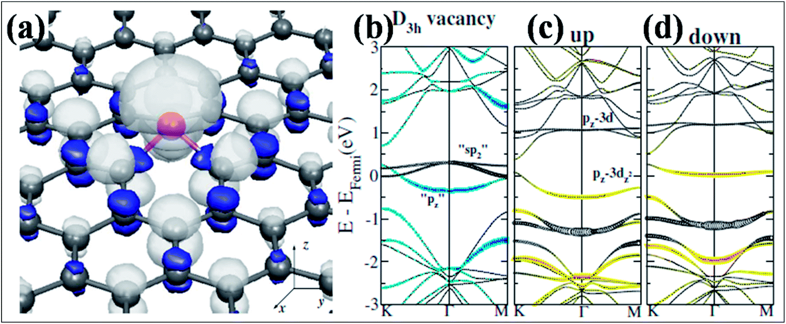 | ||
| Fig. 22 (a) Isosurface of the spin polarization produced by Co substitutional defects. Light and dark surfaces correspond to positive and negative spin densities, respectively. (b) Spin-unpolarized band structure of an unreconstructed D3h carbon vacancy. The size of the filled symbols shows the contribution of the pz orbitals of the C atoms surrounding the vacancy, while empty symbols represent sp2 character. (c) and (d) show the majority and minority spin band structures of a Co impurity in a similar cell, respectively. The sizes of the filled and empty circles indicate the respective contributions from hybridized Co 3dz2–C 2pz and Co 3d–Csp2 character. The Fermi level is set to zero. Reproduced with permission.269 © 2010 American Physical Society. | ||
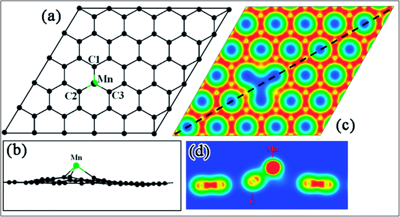 | ||
| Fig. 23 (a) Top view of the structure of Mn-substituted graphene. (b) Side view of the optimized configuration. (c) Charge density plot on the x–y plane. (d) The charge densities on the section plane along the black dashed line plotted in (c). Reproduced with permission.272 © 2010 American Chemical Society. | ||
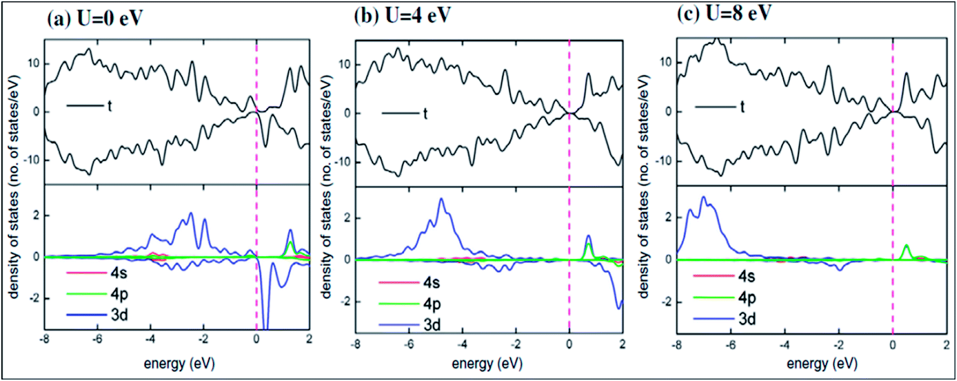 | ||
| Fig. 24 (a–c) DOS plots of the Mn-substituted graphene system at U = 0, 4 and 8 eV with the PDOS patterns of the 4s, 4p and 3d orbitals of the Mn atom. Reproduced with permission.272 © 2010 American Chemical Society. | ||
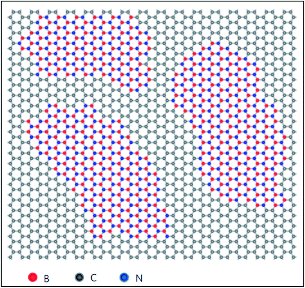 | ||
| Fig. 25 Atomic model of h-BNC film showing hybridized h-BN and graphene domains. Reproduced with permission.279 © 2010 Nature Publishing Group. | ||
4.6 Substitution of two elements (dual-doping)
Graphene substituted by two different atoms, also termed as dual-doping, has been studied to achieve and tune new and improved electronic and magnetic properties. Graphene dually doped with B and N atoms, which have similar sizes and different electronegativities (B = 2.04, N = 3.4) compared to C (2.55), shows four different bonding configurations with different bond lengths, i.e. C–C (1.42 Å), B–N (1.45 Å), C–B (1.49 Å) and C–N (1.35 Å). The binding energies of C–B and C–N are found to be lower than those of C–C and B–N, where the larger binding energy of B–N bond leads to BN-doped graphene.277 The thermal stability of BN dual-doped graphene is confirmed to be higher than that of individually doped B-G and lower than that of N-G.278 The atomic structure model of CVD-developed BN dual-doped graphene is presented in Fig. 25; the structure is simply a sp2 hybridized lattice with heteroatom BN-domains surrounded by graphene domains. The conductivity of this system is found to be dependent on the C percentage and can be tuned between insulation and high conductivity.279 BC2N and h-BN doped graphene reveal a p-type semiconducting nature.279,280 Furthermore, a hole and electron mobility of 5 to 20 cm2 V−1 s−1 accompanied by a small band gap of 18 meV is reported for h-BN substituted graphene.279 The Fermi level shifts are opposite for individual N and B doping of graphene; however, for their dual-doping of graphene, it is suggested that the band gap can be opened without shifting the Fermi level.277 The band gap opening is reported to be due to the breaking of symmetry by BN-doping281 and also by the BN domain size.282 Furthermore, band gap tuning of graphene has been theoretically observed by dual-doping of boron/lithium (B–Li)283 and boron/beryllium (B–Be)284 in graphene. The band gap size was found to be dependent on the dopant concentration283,284 and dopant sites in the hexagonal graphene lattice.284 The corresponding optimized geometries and band structures are depicted in Fig. 26(a–d)283 and Fig. 26(e–g), respectively.284 Theoretical calculations of N-S-dual-doped graphene for five different dopant configurations are shown in Fig. 27(b). The configuration where two S and N atoms simply replace two carbon atoms is declared to be the most stable. However, no bonding is found between N and S. The electronic properties and band gap opening were found to be dependent on the dopant configuration. Moreover, this material exhibits semiconducting magnetic properties and good reactivity towards molecular oxygen absorption to form SO2.285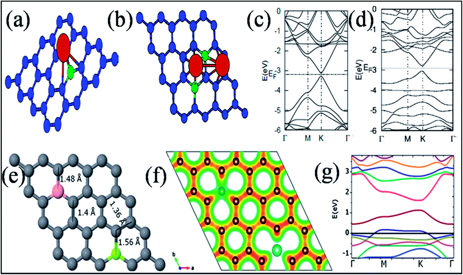 | ||
| Fig. 26 Upper panel: (a, b) Optimized structures and (c, d) band structures of a graphene sheet dual-doped by (B-Li) with increasing concentrations of B followed by adsorption of the same amount of Li. C, B and Li atoms are depicted as blue, green and brown balls, respectively. Reproduced with permission.283 © 2015 American Scientific Publishers. (e) The optimized structure of graphene dual-doped with one Be (green) and one B (pink) atom (f); charge density plot. (g) The band structure of the optimized geometry. Reproduced with permission.284 © 2015 Royal Society of Chemistry. | ||
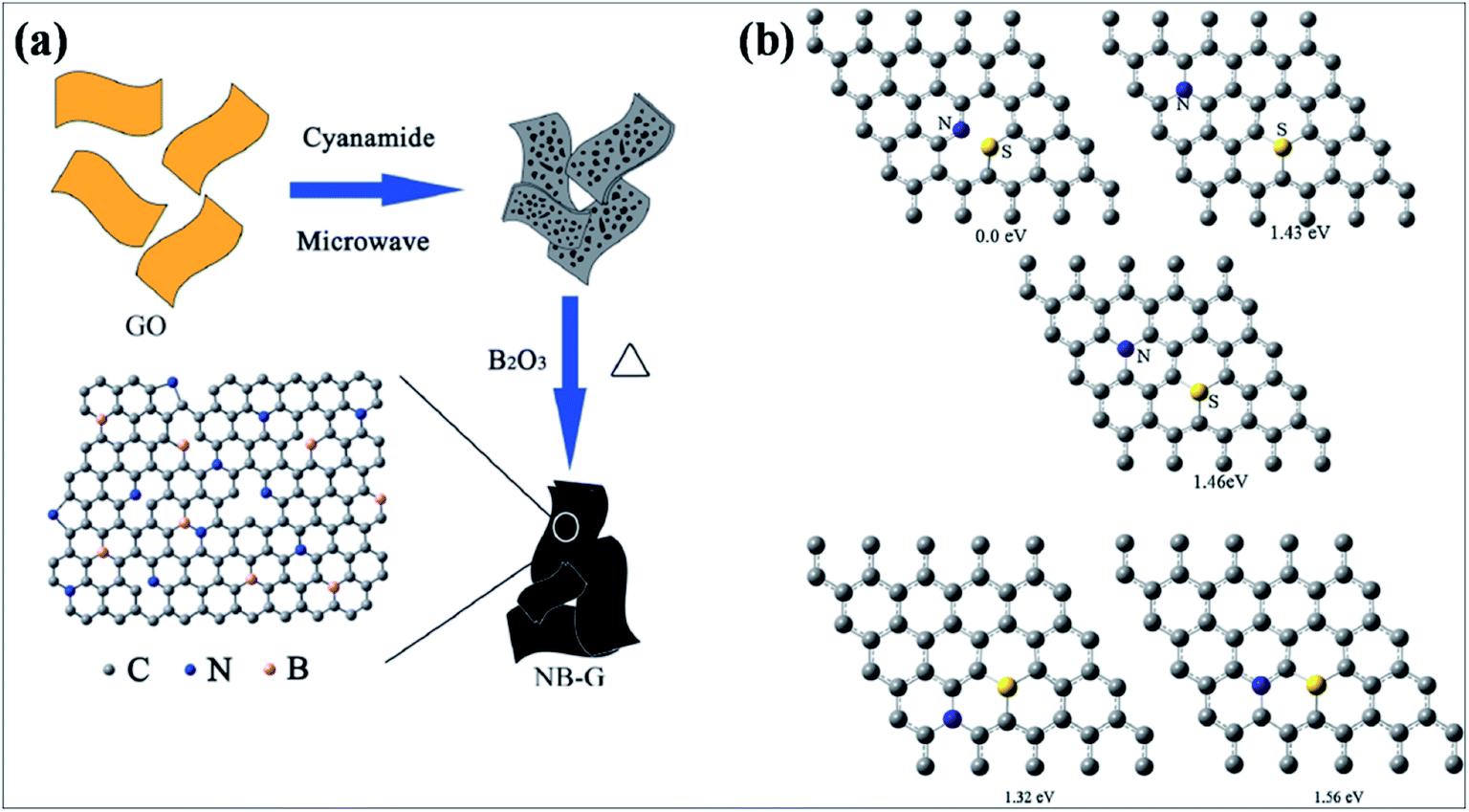 | ||
| Fig. 27 (a) Fabrication of the NB-G framework from GO. Reproduced with permission.287 © 2013 Royal Society of Chemistry. (b) Optimized unit cells for 5 × 5 sulfur and nitrogen dual-doped graphene. Reproduced with permission.285 © 2014 Elsevier. | ||
BN dual-doped graphene has been synthesized using a two-step doping method that avoids the direct combination of B and N atoms. During this process, N-G was first obtained by annealing GO in the presence of ammonia; this was further annealed in the presence of boric acid to obtain the final product, i.e. BN dual-doped graphene, which showed efficient electrocatalytic performance for the ORR.286 Theoretically, it has been proven that BN dual-doped graphene supports the adsorption of nearby oxygen-containing molecules, such as water. A microwave-assisted technique in the presence of GO (graphene source), cynamide (N source) and B2O3 (boron source) has been utilized to prepare BN dual-doped graphene, as shown in Fig. 27(a).287 The resulting product revealed a sufficient, active surface area and superior conductivity; it has potential applications in enzyme-free biosensors. Electrochemical tests of H2O2 showed good results for BN dual-doped graphene compared to individual B or N-doped graphene. A very sensitive and stable H2O2 sensor is developed, which is found to be successful in the detection of H2O2 in living cells.287
N-S dual-doped graphene incorporated with carbon black was prepared through annealing of graphene oxide, thiourea and acidized carbon black (CB).288 The obtained material demonstrated efficient catalytic activity. This enhancement is attributed to the incorporation of dopants and the increase in interlayer separation due to the presence of carbon nanospheres.288 A N-S dual-doped catalyst was prepared by argon thermal annealing of polydopamine (PDA)-functionalized and cysteine-grafted graphene oxide (GO).289 This material was found to be efficient with respect to working stability and methanol tolerance.289 A microwave-assisted technique was used for the synthesis of a N-S dual-doped graphene electrode, which was further used for the development of an artificial muscle.290 Due to their large surface areas, good conductivity, reactivity, stability, enhanced electrochemical performance and good Li ion storage capability, N–S,291,292 N–F,293 N–Cl294 and N–P295,296 dual-doped graphene materials have been proven to be excellent electrodes for batteries and292–294,296 supercapacitors294,295 as well as superior catalysts.293,297
4.7 Concluding remarks and future outlook
We have discussed the modulation of the electronic structure and magnetic properties of graphene by substitution with one or two atoms. Substitutional doping into the carbon lattice with electron-withdrawing or electron-donating heteroatoms enables tailoring of the structural, electronic, magnetic and electrochemical properties of graphene. Many novel and improved properties have been developed via substitutional doping of graphene; these properties vary with the type, concentration and size of the dopant. The newly developed materials show good potential for practical applications. B, N, S and P are the most widely used substituent atoms in graphene. Substituted B atom does not change the hexagonal sp2 planar characteristics of graphene. However, the B–C ≈ 1.50 Å bond is found to be longer than the C–C bond of pristine graphene, which leads to alteration of the lattice parameters. Graphene reveals p-type doping via individual substitution of B, S, pyridinic and pyrrolic N-G and dual-substituted BC2N and h-BN; it reveals n-type doping for P and graphitic N-G. Band gap opening in graphene via B, N, Si and P substitution was found to be sensitive to doping concentration. However, the size of the band gap was also found to be influenced by the number of layers and the arrangement of the B-dopant with respect to the superlattice symmetry. Band gap opening was also reported due to symmetry breaking by BN-doping and the size of the BN domains. In the case of N–S, the electronic properties and band gap opening were found to be dependent on the dopant configuration. S-substituted graphene can act either as a metal or small band gap semiconductor. The resulting behavior is also found to be dependent on the concentration of sulfur atoms. BC2N, h-BN and N–S materials exhibit semiconducting magnetic properties.Weak magnetism is suggested by theoretical calculations on a B-doped graphene system. Group VA and transition element substitution induces spin polarization and a magnetic moment in graphene, while N-G produced via self-propagating high-temperature synthesis (SHS) shows ferromagnetic properties at high Curie temperatures. However, anomalous magnetic behavior is observed for group VIA elements. Along with high room temperature ferromagnetism for GO and rGO, diamagnetism, paramagnetism, superparamagnetism and antiferromagnetism have been reported. Although different synthesis procedures and characterization techniques have been adopted to modulate the electronic and magnetic properties of graphene through substitution, large scale commercialized production of substitutionally doped graphene has not yet been achieved. This requires new efficient methods as well as modification of existing methods. Because the band gap in many substitutional cases depends on the concentration and configuration of dopant in the graphene lattice, experimentalists are facing challenges related to good control of dopant contents at specific positions. Control over the dopant content and doping level at a specific position, along with unperturbed intrinsic electron mobility of graphene, are the necessities of FETs, which must be resolved in the near future. Different structural configurations of N-G are challenges for both experimentalists and theoreticians, as their precise and controlled distribution has not yet been achieved. Current understanding of the correlation of heteroatoms to the carrier density, band gap opening, and electrocatalytic and photocatalytic activity of graphene is not sufficient. Obviously, the true nature of substituted graphene, whether metallic or semiconducting, remains unresolved.
5. Modulation via creation of vacancies and its applications
Different types of defects can appear in the graphene lattice during its growth or irradiation processes. The most common defects are lattice vacancies in the graphene structure, which cause significant changes to the structural, electronic and magnetic properties of graphene. Many theoretical studies have been devoted to the diffusion of vacancies and the structural changes produced thereby in the graphene lattice.298–300 The graphene bipartite lattice can be seen as two interpenetrating sublattices of carbon atoms. For the creation of vacancies in the first lattice, only the pz orbitals of the second lattice carbon atoms contribute to the localized states. The presence of vacancies creates Jahn–Teller distortion in the graphene lattice.298,299,301,302 The magnetic moment arising from a single vacancy (SV) is attributed to the presence of unpaired electrons created by the removal of a carbon atom.298 Moreover, it is considered that for SV, the total magnetic moment is the sum of the magnetic moment (1 μB) localized at the σ bands and a fractional value of the extended π bands. The magnitude of the magnetic moment is found to be sensitive to defect concentration, separation between vacancies,299,303 the passivation of dangling σ bonds and unpassivated σ bonds.301 DFT spin polarized calculations for a single vacancy showed that the presence of the vacancy produces a pentagon-like structure due to the formation of a weak covalent bond between two atoms surrounding the vacancy. Among the three dangling bonds of a vacancy surrounded by three atoms, two undergo saturation due to the formation of the pentagon, while the third bond plays a key role in the creation of the magnetic moment (1.04 μB) in pure non-magnetic graphene.298 The difference of 0.1 eV between the magnetic and non-magnetic ground state energies298,302 provides evidence for the unstable magnetism induced by a single C vacancy, which can be decreased by a finite temperature and through interlayer interactions. The theoretically predicted values for the single vacancy-induced magnetic moment in graphene range from 1 to 2 μB.298,301,304 The experimentally determined magnetic moments137,305 of vacancy graphene and traces of room temperature ferromagnetism305–307 are still disputatious and debatable.Experimental308 and theoretical299,309 studies have been conducted to explore the data of STM images in order to understand the nature of vacancies in graphene. However, two types of conformer, D3h-symmetry and Cs-symmetry, have been observed from these calculations;309 these are shown in Fig. 28(a) and (b), respectively. For the simulated image of a Cs-symmetry type vacancy, it can be seen from Fig. 28(b) that the structure is perturbed so that among the three neighboring atoms of the vacancy, two come closer to each other, while the third atom goes out of plane with a certain displacement.309 Moreover, the STM image (Fig. 28(c–e)) of the D3h single vacancy shows trigonal symmetry at the center of the C vacancy, which develops due to the localization of the electronic states of the three dangling bonds. The reconstructed Cs-symmetry vacancy is no longer described by three-fold symmetry. The trigonal symmetry of the lattice was observed to be restored due to rotation of the pentagon by ±2π/3 for a Cs vacancy. The band structure and magnetic properties of graphene are sensitive to the presence of both types of defects. The obtained band structures in the presence of Cs (Fig. 28(f)) and D3h (Fig. 28(g)) vacancies are presented. The presence of a vacancy breaks the lattice and sublattice symmetry and perturbs the π-orbital of pristine graphene, which results in band gap opening at the Dirac point. For Cs-symmetry vacancy defects, the π-band gap is larger than the D3h-symmetry vacancy. The presence of an additional induced flat σ-band close to the Fermi level is due to the localization of defective states on the C-atoms surrounding the vacancy. Due to the breaking of symmetry by the Cs-symmetry vacancy, one σ band moves deeper into the valence band. Moreover, the π-band is shifted upward with respect to the position of the Fermi level.
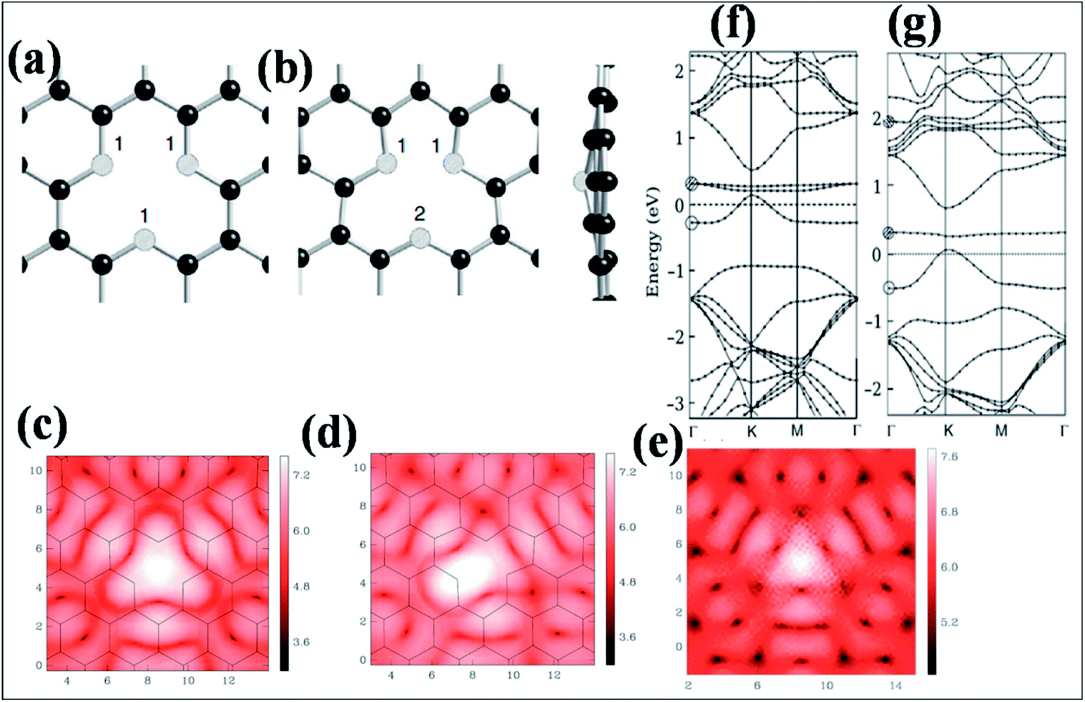 | ||
| Fig. 28 (a) Top view of a fully relaxed non-reconstructed vacancy (D3h-symmetry of graphene). (b) Top and side views of the reconstructed vacancy with Cs-symmetry. (c–e) STM computed images for the single C-vacancy in graphene with a positive tip potential of 0.2 V. (c) D3h vacancy; (d) Cs vacancy. (e) Average of the three equivalent Cs structures rotated by ±2π/3. (f, g) Comparison of the DFT-LDA calculated band structures of graphene with mono-vacancies of different symmetries: (f) D3h symmetry and (g) Cs symmetry. The shaded and empty circles respectively indicate the σ and π bands. The Fermi level is set to zero. Reproduced with permission.309 © 2007 American Physical Society. | ||
For both spin and non-spin polarized calculations of graphene with a single vacancy, the trend of total energy as a function of different relaxed final displacements of the 3rd out of plane displaced carbon atom is depicted in Fig. 29(a) and (b). These results show a planar and spin polarized ground state for graphene. The larger shift of energy after a displacement of 0.20 Å to the metastable state transforms the system to a non-magnetic state, which is due to the loss of connection of the π-electron released by the vacancy to the 2D-electron network. The same trend is depicted in Fig. 29(c).302
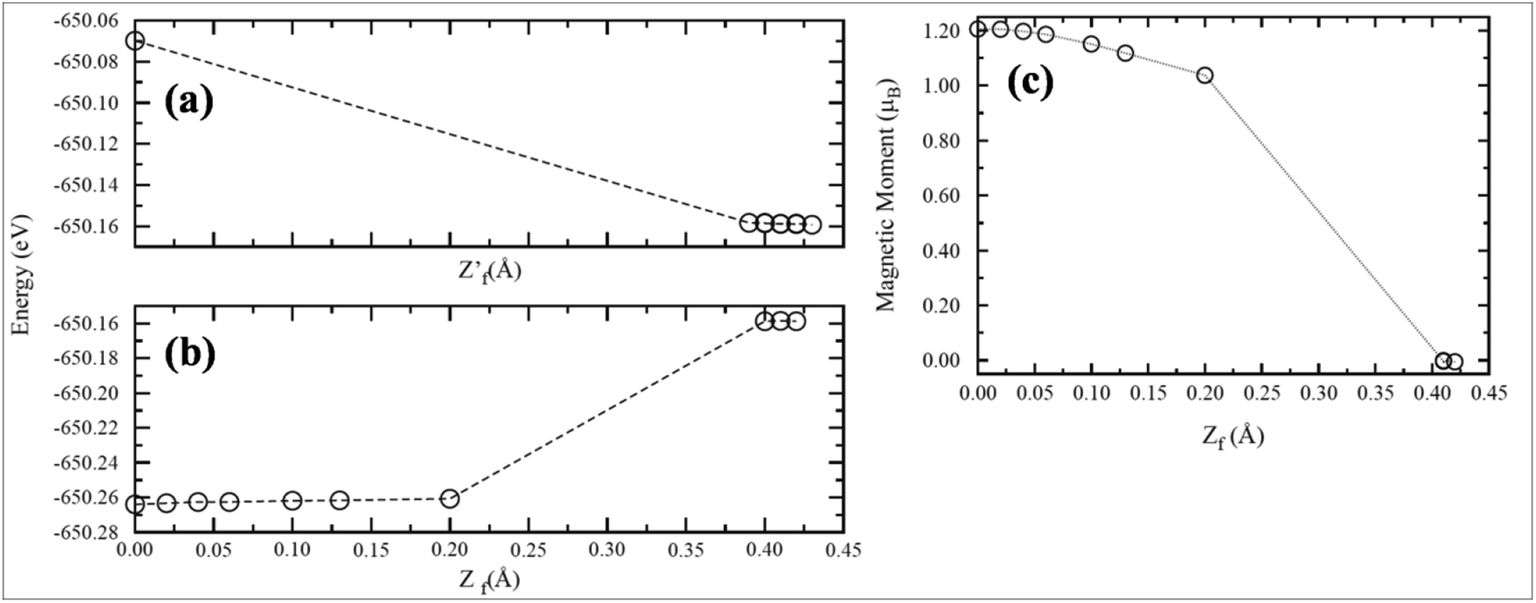 | ||
| Fig. 29 Total energy of a graphene sheet with a SV calculated as a function of the displacement of atom 3 perpendicular to the sheet (a) without spin polarization and (b) with spin polarization. (c) Magnetic moment of the graphene sheet with a SV calculated as a function of the displacement of atom 3 perpendicular to the sheet for the relaxed structure. Reproduced with permission.302 © 2013 Elsevier. | ||
The presence of more than one vacancy and their mutual relationship greatly alter the magnetization phenomenon in graphene.302,304,310 The arrangement and distribution of vacancies over perfectly balanced graphene create sublattice imbalance, which leads to magnetization in graphene.301 The alteration of the band gap via vacancies is presented in Fig. 30. It can be seen in Fig. 30(c) that the band gap is concealed by the presence of two identical vacancies present in different sublattices due to the restoration of the sublattice symmetry. However, a larger band gap (Fig. 30(b)) can be seen for the presence of two identical vacancies on the same sublattice.311
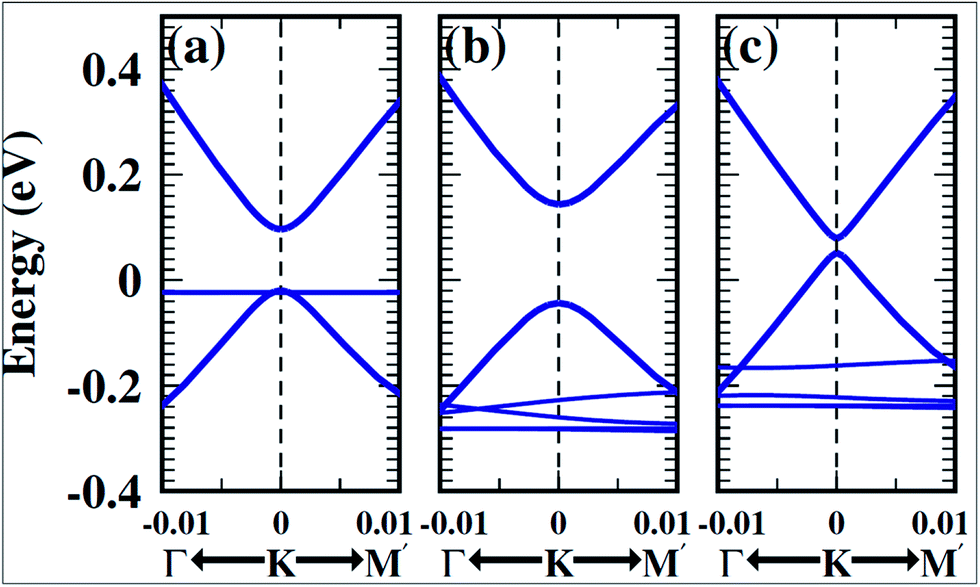 | ||
| Fig. 30 The band structure plots of (a) single vacancy graphene sheets; (b, c) two identical vacancies present at the same and different sublattice sites, respectively. The Dirac point energy of pristine graphene is set to zero. Reproduced with permission.311 © 2008 American Physical Society. | ||
Furthermore, research has also been conducted on hydrogenated SV in graphene, in which either one or two of a total of three under-coordinated carbon atoms surrounding the vacancy are saturated with hydrogen.294,298,301 A magnetic moment of 2.3 μB is reported for hydrogen saturation of a single vacancy-created dangling bond. However, a magnetic moment of 1.2 μB is reported for a stable magnetic configuration, shown in Fig. 31, for the hydrogen saturation of a graphene single vacancy, which is already saturated with hydrogen.298
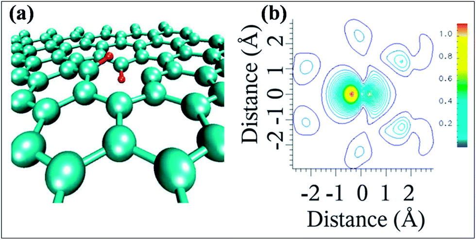 | ||
| Fig. 31 (a) Structure and (b) spin density (μB/E2) of a vacancy surrounded by two hydrogens. Reproduced with permission.298 © 2004 American Physical Society. | ||
A collective experimental and theoretical study of a divacancy in graphene presented a dangling bond-free non-hexagonal rearranged flat structure. Moreover, no magnetic traces were observed for this divacancy system.312 A comparison of the dissociative absorptions of the H2 molecules on pristine and mono-vacancy graphene demonstrated vacant graphene to be a good dissociative absorber for H2 molecules. This enhancement in absorption is attributed to a decrease of the dissociative energy barrier of H2 molecules on graphene in the presence of vacancies. The band structure and electronic properties of the pristine graphene are altered due to the presence of vacancies and H2 adsorption. Furthermore, different vacancy concentrations created the same perturbations in pristine graphene, which shows that dissociative adsorption and detection of low concentrations of hydrogen is independent of the vacancy concentration in graphene sheets.313 Hydrogen sulfite (H2S) molecules bind more strongly to vacancy-containing graphene than to pristine graphene. A comparison of the DOS of pristine graphene, H2S/pristine graphene, vacancy graphene and H2S/vacancy graphene systems is shown in Fig. 32. It is clear (Fig. 32(b)) that vacancy graphene exhibits metallic characteristics, while H2S/vacancy graphene exhibits semiconductor characteristics. This strong interaction of H2S and vacancy graphene suggests that vacancy graphene can be used in H2S sensors.314
 | ||
| Fig. 32 Representation of the electronic density of states of (a) pristine and H2S/pristine graphene systems; (b) defect-graphene and H2S/defect-graphene systems. Reproduced with permission.314 © 2013 Elsevier. | ||
5.1 Concluding remarks and future outlook
Different types of defects can appear in the graphene lattice during its growth or irradiation processes. The most common defects are lattice vacancies in the graphene structure; these cause significant changes to the structural, electronic and magnetic properties of graphene. The graphene bipartite lattice can be seen as two interpenetrating sublattices of carbon atoms. Removal of a C atom from the graphene lattice results in sublattice imbalance due to the difference in the number of atoms of the individual sublattices. This creates Jahn–Teller distortion in the graphene lattice. Among the three dangling bonds of the three atoms surrounding the vacancy, two undergo saturation due to the formation of a pentagon, while the third bond participates in the creation of a magnetic moment in non-magnetic graphene. It is considered that for SV, the total magnetic moment is the sum of 1 μB localized at the σ bands and a fractional value of the extended π bands. Moreover, the magnitude of the magnetic moment is found to be sensitive to defect concentration, separation between vacancies, the passivation of dangling σ bonds and unpassivated σ bonds. Experimentally, problems related to control of the passivation of graphene edges, such as allowing only the passivation of σ bonds and avoiding the passivation of π bonds, are unresolved. Although many techniques have been utilized to create locally and commercially imbalanced graphene lattices, this challenge remains. Theoretically predicted values for the single vacancy-induced magnetic moment in graphene range from 1 to 1.7 μB. Experimentally, determinations of the magnetic moment of defective graphene and traces of room temperature ferromagnetism are still limited. The reasons for these difficulties in the observation of ferromagnetism in graphene and graphene-based systems are poorly understood and remain debatable.6. Modulation via edges and strain and their applications
6.1 Modulation via edges (size confinement)
One-dimensional structures with nano-scaled widths, also known as graphene nano-ribbons (GNRs), can be achieved by cleaving graphene along a specific direction. Due to this cleaving in a specific direction, the edge C atoms of GNRs adopt two topological shapes, known as armchair and zigzag. The characteristics of GNRs are governed by the exact natures of their edges.315,316 GNRs are synthesized by different techniques, such as top down (unzipping of CNTs),317 bottom up,318 CVD,319 sonochemical,318 electron beam lithography and plasma etching.320 The topology and width of GNRs prepared via the sonochemical technique are found to be influenced by the structure and functionality pattern of the precursor monomers.318 Theoretical studies show that the electronic and magnetic properties of graphene strongly depend on the configuration of its atomic edges.315,321 The properties of GNRs are quite different from those of graphene. The perfect symmetrical structure of graphene is broken by the edges of GNRs.315 It has been proved both theoretically316 and experimentally320,322 that GNRs have finite band gaps. The band gaps generated in GNRs are dependent on the orientation and width of their edges, whereas the structure and degree of the edge termination influence the functionality of GNRs. Theoretical studies predict that zigzag graphene nanoribbons (ZGNRs) are metallic and have special localized edge states which are antiferromagnetically coupled between the two edges, while armchair graphene nanoribbons (AGNRs) are nonmagnetic and semiconducting.323,324 Theoretically, the bare zigzag edges are predicted to be less stable than the armchair edges. Under ambient circumstances, reconstruction into pentagon–heptagon structures occurs.315 For practical purposes, hydrogen saturation is usually performed to stabilize both armchair and zigzag graphene edges.315Graphene edges are very reactive and are influenced by the ribbon width and the orientations of C atoms at their edges. GNRs are more reactive than bulk single graphene sheets. ZGNRs show higher chemical reactivity than AGNRS.315 The greater chemical reactivity of ZGNRs is due to the presence of unpaired π-electrons on their edges.315,325 DFT calculations have been used to explore the mechanism of band gap and magnetism formation in 8-ZGNR/h-BN(0001) heterostructures. These calculations revealed a band gap of 380 meV. A local magnetic moment of 0.27 μB is found for edge C atoms, which is greater than that of the basal atoms.326 Furthermore, it was shown that the charge carrier mobility of ZGNR/h-BN(0001) heterostructures is 5% higher than that of suspended nanoribbons.327
The edges of GNRs play a key role in the modulation of their electronic properties. Structural modification of the edges, such as bond reconstruction, edge functionalization, passivation, doping and strain, lead to alteration of the π-network at the edges. These structural modifications are potential methods to tailor the geometries, stability, electronic properties, spin polarization, spin gap asymmetry and size of the band gap of graphene.315,325,328 A wide range of atoms and chemical groups have been used to functionalize the edges of graphene.315,325,327 By considering –H, –F, –Cl, –Br, –S, –SH, and –OH as edge-functional groups, band gap tuning of ∼1.2 eV is observed for AGNRs. The band gap of ZGNRs is found to be influenced by the ribbon width.329 In theoretical calculations, half-metallicity of ZGNRs is realized by modifying their edges with a pair of donor and acceptor (CH3–NO2) functional groups.330 Furthermore, it is proposed that half-metallicity in ZGNRs can be obtained by functionalizing the edge of one side with hybrid X groups (X = SO2, NO2, CN) and H atoms.331
Doping is also a possible method to modify the electronic properties of GNRs.332,333 Calculations revealed that the electronic properties of N-doped ZGNRs are dependent on the doping site.332 It was shown that doping with different groups can lead to metal–semiconductor transitions.332,333 Single N atom substitution and pyridine and pyrrole-like N-doping defects can all break the degeneracy of the spin polarization of pristine ZGNRs. Substitution of a single N atom transforms the antiferromagnetic semiconducting ZGNRs into spin gapless semiconductors, while substitution of N on both edges transforms ZGNRs into non-magnetic metals. Furthermore, ZGNRs adopt half metallic or spin gapless semiconductor natures by substitution of pyridine and pyrrole-like N-doping defects.333
Extensive investigations of GNRs have revealed the potential of these structures in high performance nano-electronics, optoelectronics, spintronics, sensors, bioimaging and energy storing devices due to their unique physical properties.325,334–339 Several groups using different chemical synthesis methods reported different current on/off ratios for GNR-based FETs.325,334 Another promising application of GNRs is as an electrode material for batteries and supercapacitors.337–339 A LIB anode based on N-GNRs after 100 cycles at a current density of 0.1 A g−1 showed a retention capacity of 714 mA h g−1. The excellent rate capability of the material is attributed to the abundance of edges and doping.338 A LIB anode based on a composite of GNRS and SnO2 nanoparticles showed higher reversible discharge capacity (1130 mA h g−1) than the theoretical capacity of SnO2 (∼782 mA h g−1). After 50 cycles, a reversible capacity of ∼825 mA h g−1 was maintained at a current density of 100 mA g−1. This excellent capacity, retention and power performance is attributed to the highly ordered distribution of SnO2 NPs along the GNRs.339
6.2 Modulation via strain
Graphene has been proved to be the thinnest and strongest 2D material ever measured. Strain is usually expected to arise unintentionally in experimental synthesis of graphene. Graphene usually experiences strain due to surface corrugation of the substrate or finite sheet lattice mismatch between graphene and the substrate.340 The deviation of the finite sheet from the ideal bulk structure in the locality of an edge results in either tensile or compressive stress near the edge.341 Experimental and theoretical studies have revealed ripples in flat graphene sheets due to thermal effects.342,343 In addition to intrinsic strain, extrinsic strain can also be induced and controlled in graphene by different techniques.344,345Calculations revealed that the application of strain can modify the band structure and electronic properties of graphene.345–347 The shifting of the Dirac cones (located at the K and K′ points) occurs in opposite directions under the application of uniaxial or shear strain. If sufficiently large uniaxial or shear strain is applied to graphene, the two inequivalent Dirac points, which progress away from the K and K′ points, respectively, may approach each other and eventually merge, leading to band gap opening in the graphene. This type of gap induced by the merging of the Dirac cones has been reported by theoretical calculations.346,348 Electronic structure calculations of graphene demonstrated that application of tensional strain can produce a bulk spectral gap, which suggests a new method to alter the electrical transport properties and pinch off current flows in graphene-based devices.346 Strain in graphene can be characterized by two major varieties, namely uniaxial and shear. This strain behaves differently on graphene depending on the edge shape, namely zigzag or armchair. The band gap opening of AGNRs is found to be dependent on their geometry and the applied compression. Moreover, the antiferromagnetic states of ZGNRs have been found to significantly improve with compression.345
Strain acts like a catalyst for graphene because by applying strain to the graphene, it is possible to greatly increase both its rate of reactivity and functionalization. It has also been revealed that unfavorable reactions that would not take place on relaxed graphene can be greatly enhanced by applying strain to the graphene.347,349 It was demonstrated that graphene which is deformed by contact with SiO2 nanoparticles displays enhanced reactivity toward aryl diazonium functionalization, which is attributed to the strain and the localized areas of increased curvature induced by the strain.349 Theoretical calculations suggest that waved graphene is a suitable choice for the physical and chemical adsorption of H2, N2, NO and CO molecules.347 The outstanding stretchability of graphene has enabled its application in flexible electronic devices, such as touch screens, electronic papers, and foldable organic light emitting diodes (OLED).58,350
6.3 Concluding remarks and future outlook
In this section, we have discussed the effects of edges and strain on graphene. Our discussion includes the synthesis procedures of graphene edges and the effects of edges and strain on the electronic, magnetic and chemical reactivity of graphene. Studies show that the electronic and magnetic properties of graphene strongly depend on the atomic configuration of its edges. The band gaps generated in GNRs are dependent on the orientation and width of the edges, whereas the structure and degree of the edge termination influence the functionality of GNRs. Structural modification of the edges, such as bond reconstruction, edge functionalization, passivation, doping and strain, lead to alteration of the π-network at the edges. These structural modifications are possible methods to tailor the properties of graphene.Among all synthesis procedures, cutting of CNTs is the best technique for the mass production of high quality GNRs. However, different structural parameters of the CNTs, such as their diameter, number of concentric cylinders and chirality, significantly influence the width and smoothness of the graphene edges. To address this issue, new techniques are required to produce CNTs with narrow diameters, fixed concentric cylinders and specific chiralities. The main disadvantage which hinders the potential applications of lithographic patterns followed by plasma etching is width control of the nanoribbons and roughness of the edges. Although the field of graphene nanoribbons has been widely developed, some issues remain to be addressed, such as the width, smoothness and quality of the ribbons; these should be investigated in more detail and improved in the near future. Moreover, the improvement of these parameters will lead to increased research activities on the functionalization of GNRs. Although theoretical calculations have been successful in exploring the essential features of bare and functionalized graphene edges, clear observation and modulation of perfect freely suspended graphene edges at the atomic scale remains difficult to achieve.
Graphene usually experiences strain due to surface corrugation of the substrate or finite sheet lattice mismatch between graphene and the substrate. Extrinsic strain can be induced and controlled in graphene by different techniques. It has been proved that the application of strain can modify the band structure of graphene, thus altering its electronic properties. Strain behaves differently on zigzag and armchair edges of graphene. Strain acts like a catalyst for graphene. Strain engineering provides a way to further explore both novel physical phenomena in graphene and its potential integration into a variety of devices. Although many studies have been carried out on strained graphene, enormous efforts are still required to clarify the underlying mechanism and to achieve commercial use of graphene-based devices.
7. Summary
Graphene, a sp2 hybridized single layer of hexagonally arranged carbon atoms, is considered to be a zero band gap semiconductor or semimetal. This 2D material has gained increasing attention in recent exhaustive studies due to its novel properties, such as high charge carrier mobility, high optical transparency and mechanical strength. Due to these properties, graphene is a promising material for electronic devices and transparent electrodes in optoelectronics. In pristine form, its potential is restricted by its zero band gap, non-magnetic nature. In order to take full advantage of the hidden potential of this material, many techniques have been adopted to tailor its electronic and magnetic properties. These methods include interaction of graphene with the substrate, adatom adsorption, substitutional doping and vacancy defects. Herein, we have overviewed recent techniques adopted to tailor the electronic and magnetic properties of graphene and the possible practical applications of these techniques in diverse fields of research. Furthermore, the challenges faced by individual techniques are also included. Overall, it can be concluded that every atom of graphene is a surface atom. Thus, it is difficult to control its interactions with the substrate and the surrounding environment.As the zero band gap characteristics of graphene are due to its symmetry, charge or spin imbalance between the sublattices of graphene can be created by its interaction with the substrate, which alters the graphene lattice and hence its electronic and magnetic properties. Furthermore, vacancies, surface doping by adsorption, substitutional doping, edges and strain can manipulate and improve the structural, electronic, magnetic, electrochemical and physicochemical properties of graphene, which are found to be dependent on the number of vacancies, vacancy configuration, dopant type, concentration and configuration, type of edge, and the magnitude and type of strain. All the mentioned processes have been proven to have remarkable potential in different fields, such as electronics, transparent electrodes, energy storage and conversion devices, sensors and biomedicine.
Conflicts of interest
There are no conflicts to declare.Acknowledgements
This research was supported by NSFC (No. 51371112), the innovation program of Shanghai Municipal Education Commission (No. 2014CB643403), and the National Science Fund for Distinguished Young Scholars of China (No. 51225401).References
- K. S. Novoselov, A. K. Geim, S. V. Morozov, D. Jiang, Y. Zhang, S. V. Dubonos, I. V. Grigorieva and A. A. Firsov, Science, 2004, 306, 666–669 CrossRef CAS PubMed.
- K. I. Bolotin, K. Sikes, Z. Jiang, M. Klima, G. Fudenberg, J. Hone, P. Kim and H. Stormer, Solid State Commun., 2008, 146, 351–355 CrossRef CAS.
- K. S. Novoselov, Z. Jiang, Y. Zhang, S. Morozov, H. L. Stormer, U. Zeitler, J. Maan, G. Boebinger, P. Kim and A. K. Geim, Science, 2007, 315, 1379 CrossRef CAS PubMed.
- D. Jariwala, V. K. Sangwan, L. J. Lauhon, T. J. Marks and M. C. Hersam, Chem. Soc. Rev., 2013, 42, 2824–2860 RSC.
- B. H. Nguyen and V. H. Nguyen, Adv. Nat. Sci.: Nanosci. Nanotechnol., 2016, 7, 013002 CrossRef.
- W. Lv, Z. Li, Y. Deng, Q.-H. Yang and F. Kang, Energy Storage Materials, 2016, 2, 107–138 CrossRef.
- N. Mahmood, C. Zhang, H. Yin and Y. Hou, J. Mater. Chem. A, 2014, 2, 15–32 CAS.
- S. S. Varghese, S. Lonkar, K. Singh, S. Swaminathan and A. Abdala, Sens. Actuators, B, 2015, 218, 160–183 CrossRef CAS.
- Y. Shao, J. Wang, H. Wu, J. Liu, I. A. Aksay and Y. Lin, Electroanalysis, 2010, 22, 1027–1036 CrossRef CAS.
- S. Kumar and K. Chatterjee, ACS Appl. Mater. Interfaces, 2016, 8, 26431–26457 CAS.
- R. Zhou and H. Gao, WIREs Nanomed. Nanobiotechnol., 2014, 6, 452–474 CrossRef CAS PubMed.
- S. Y. Zhou, G.-H. Gweon, A. Fedorov, P. First, W. De Heer, D.-H. Lee, F. Guinea, A. Neto and A. Lanzara, Nat. Mater., 2007, 6, 770 CrossRef CAS PubMed.
- J. Jung, A. M. DaSilva, A. H. MacDonald and S. Adam, Nat. Commun., 2015, 6, 6308 CrossRef CAS PubMed.
- A. Mattausch and O. Pankratov, Phys. Rev. Lett., 2007, 99, 076802 CrossRef PubMed.
- T. Ohta, A. Bostwick, T. Seyller, K. Horn and E. Rotenberg, Science, 2006, 313, 951–954 CrossRef CAS PubMed.
- E. McCann and V. I. Fal’ko, Phys. Rev. Lett., 2006, 96, 086805 CrossRef PubMed.
- I. Shtepliuk, V. Khranovskyy, R. Yakimova, H. Qing-Song, G. Li-Wei and W. Wen-Jun, Jpn. J. Appl. Phys., 2016, 55, 08NB02 CrossRef.
- X. Shan, Q. Wang, X. Bian, W.-q. Li, G.-h. Chen and H. Zhu, RSC Adv., 2015, 5, 78625–78633 RSC.
- X. Peng and R. Ahuja, Nano Lett., 2008, 8, 4464–4468 CrossRef CAS PubMed.
- T. Mendes-de-Sa, A. Goncalves, M. Matos, P. Coelho, R. Magalhaes-Paniago and R. Lacerda, Nanotechnology, 2012, 23, 475602 CrossRef CAS PubMed.
- J. Hass, F. Varchon, J.-E. Millan-Otoya, M. Sprinkle, N. Sharma, W. A. de Heer, C. Berger, P. N. First, L. Magaud and E. H. Conrad, Phys. Rev. Lett., 2008, 100, 125504 CrossRef CAS PubMed.
- Z.-j. Wang, M. Wei, L. Jin, Y. Ning, L. Yu, Q. Fu and X. Bao, Nano Res., 2013, 6, 399–408 CrossRef CAS.
- Y.-M. Lin, C. Dimitrakopoulos, K. A. Jenkins, D. B. Farmer, H.-Y. Chiu, A. Grill and P. Avouris, Science, 2010, 327, 662 CrossRef CAS PubMed.
- P. Avouris and F. Xia, MRS Bull., 2012, 37, 1225–1234 CrossRef CAS.
- Z. Guo, R. Dong, P. S. Chakraborty, N. Lourenco, J. Palmer, Y. Hu, M. Ruan, J. Hankinson, J. Kunc and J. D. Cressler, Nano Lett., 2013, 13, 942–947 CrossRef CAS PubMed.
- Y.-M. Lin, A. Valdes-Garcia, S.-J. Han, D. B. Farmer, I. Meric, Y. Sun, Y. Wu, C. Dimitrakopoulos, A. Grill and P. Avouris, Science, 2011, 332, 1294–1297 CrossRef CAS PubMed.
- M. W. Nomani, R. Shishir, M. Qazi, D. Diwan, V. Shields, M. Spencer, G. S. Tompa, N. M. Sbrockey and G. Koley, Sens. Actuators, B, 2010, 150, 301–307 CrossRef CAS.
- S. Novikov, A. Satrapinski, N. Lebedeva and I. Iisakka, IEEE Trans. Instrum. Meas., 2013, 62, 1859–1864 CrossRef CAS.
- C. X. Lim, H. Y. Hoh, P. K. Ang and K. P. Loh, Anal. Chem., 2010, 82, 7387–7393 CrossRef CAS PubMed.
- S. Bae, H. Kim, Y. Lee, X. Xu, J.-S. Park, Y. Zheng, J. Balakrishnan, T. Lei, H. R. Kim and Y. I. Song, Nat. Nanotechnol., 2010, 5, 574–578 CrossRef CAS PubMed.
- W. Strupinski, K. Grodecki, A. Wysmolek, R. Stepniewski, T. Szkopek, P. Gaskell, A. Gruneis, D. Haberer, R. Bozek and J. Krupka, Nano Lett., 2011, 11, 1786–1791 CrossRef CAS PubMed.
- A. Ambrosi and M. Pumera, J. Phys. Chem. C, 2013, 117, 2053–2058 CAS.
- D. B. Farmer, H.-Y. Chiu, Y.-M. Lin, K. A. Jenkins, F. Xia and P. Avouris, Nano Lett., 2009, 9, 4474–4478 CrossRef CAS PubMed.
- D. Prasai, J. C. Tuberquia, R. R. Harl, G. K. Jennings and K. I. Bolotin, ACS Nano, 2012, 6, 1102–1108 CrossRef CAS PubMed.
- X. Li, Y. Zhu, W. Cai, M. Borysiak, B. Han, D. Chen, R. D. Piner, L. Colombo and R. S. Ruoff, Nano Lett., 2009, 9, 4359–4363 CrossRef CAS PubMed.
- M. Ishigami, J. Chen, W. Cullen, M. Fuhrer and E. Williams, Nano Lett., 2007, 7, 1643–1648 CrossRef CAS PubMed.
- P. Shemella and S. K. Nayak, Graphene on silicon dioxide: band gap modulation via substrate surface chemistry, Bulletin of the American physical society, 2009 APS March meeting, 2009, vol. 54, number 1.
- Y. Shi, X. Dong, P. Chen, J. Wang and L.-J. Li, Phys. Rev. B: Condens. Matter Mater. Phys., 2009, 79, 115402 CrossRef.
- Y. Xu, K. He, S. Schmucker, Z. Guo, J. Koepke, J. Wood, J. Lyding and N. Aluru, Nano Lett., 2011, 11, 2735–2742 CrossRef CAS PubMed.
- D. A. Brownson, S. A. Varey, F. Hussain, S. J. Haigh and C. E. Banks, Nanoscale, 2014, 6, 1607–1621 RSC.
- R. Decker, Y. Wang, V. W. Brar, W. Regan, H.-Z. Tsai, Q. Wu, W. Gannett, A. Zettl and M. F. Crommie, Nano Lett., 2011, 11, 2291–2295 CrossRef CAS PubMed.
- S. Roth, F. Matsui, T. Greber and J. Osterwalder, Nano Lett., 2013, 13, 2668–2675 CrossRef CAS PubMed.
- G. Giovannetti, P. A. Khomyakov, G. Brocks, P. J. Kelly and J. Van Den Brink, Phys. Rev. B: Condens. Matter Mater. Phys., 2007, 76, 073103 CrossRef.
- Y. Lu, P. He and Y. Feng, J. Phys. Chem. C, 2008, 112, 12683–12686 CAS.
- C. Enderlein, Y. Kim, A. Bostwick, E. Rotenberg and K. Horn, New J. Phys., 2010, 12, 033014 CrossRef.
- E. N. Voloshina, Y. S. Dedkov, S. Torbrügge, A. Thissen and M. Fonin, Appl. Phys. Lett., 2012, 100, 241606 CrossRef.
- S.-Y. Kwon, C. V. Ciobanu, V. Petrova, V. B. Shenoy, J. Bareno, V. Gambin, I. Petrov and S. Kodambaka, Nano Lett., 2009, 9, 3985–3990 CrossRef CAS PubMed.
- E. Starodub, A. Bostwick, L. Moreschini, S. Nie, F. El Gabaly, K. F. McCarty and E. Rotenberg, Phys. Rev. B: Condens. Matter Mater. Phys., 2011, 83, 125428 CrossRef.
- J. Nam, D.-C. Kim, H. Yun, D. H. Shin, S. Nam, W. K. Lee, J. Y. Hwang, S. W. Lee, H. Weman and K. S. Kim, Carbon, 2017, 111, 733–740 CrossRef CAS.
- P. Khomyakov, G. Giovannetti, P. Rusu, G. v. Brocks, J. Van den Brink and P. J. Kelly, Phys. Rev. B: Condens. Matter Mater. Phys., 2009, 79, 195425 CrossRef.
- D. Eom, D. Prezzi, K. T. Rim, H. Zhou, M. Lefenfeld, S. Xiao, C. Nuckolls, M. S. Hybertsen, T. F. Heinz and G. W. Flynn, Nano Lett., 2009, 9, 2844–2848 CrossRef CAS PubMed.
- Y. S. Dedkov, M. Fonin, U. Rüdiger and C. Laubschat, Phys. Rev. Lett., 2008, 100, 107602 CrossRef PubMed.
- C. Praveen, S. Piccinin and S. Fabris, Phys. Rev. B: Condens. Matter Mater. Phys., 2015, 92, 075403 CrossRef.
- M. Alattas and U. Schwingenschlögl, Sci. Rep., 2016, 6, 26753 CrossRef CAS PubMed.
- J. Sun, J. B. Hannon, R. M. Tromp, P. Johari, A. A. Bol, V. B. Shenoy and K. Pohl, ACS Nano, 2010, 4, 7073–7077 CrossRef CAS PubMed.
- J. Warmuth, A. Bruix, M. Michiardi, T. Hänke, M. Bianchi, J. Wiebe, R. Wiesendanger, B. Hammer, P. Hofmann and A. A. Khajetoorians, Phys. Rev. B: Condens. Matter Mater. Phys., 2016, 93, 165437 CrossRef.
- R. Decker, J. Brede, N. Atodiresei, V. Caciuc, S. Blügel and R. Wiesendanger, Phys. Rev. B: Condens. Matter Mater. Phys., 2013, 87, 041403 CrossRef.
- K. S. Kim, Y. Zhao, H. Jang, S. Y. Lee, J. M. Kim, K. S. Kim, J.-H. Ahn, P. Kim, J.-Y. Choi and B. H. Hong, Nature, 2009, 457, 706 CrossRef CAS PubMed.
- R.-H. Kim, M.-H. Bae, D. G. Kim, H. Cheng, B. H. Kim, D.-H. Kim, M. Li, J. Wu, F. Du and H.-S. Kim, Nano Lett., 2011, 11, 3881–3886 CrossRef CAS PubMed.
- X. Li, W. Cai, J. An, S. Kim, J. Nah, D. Yang, R. Piner, A. Velamakanni, I. Jung and E. Tutuc, Science, 2009, 324, 1312–1314 CrossRef CAS PubMed.
- M. Bokdam, P. A. Khomyakov, G. Brocks, Z. Zhong and P. J. Kelly, Nano Lett., 2011, 11, 4631–4635 CrossRef CAS PubMed.
- E. Hwang, S. Adam and S. D. Sarma, Phys. Rev. B: Condens. Matter Mater. Phys., 2007, 76, 195421 CrossRef.
- K. T. Chan, J. Neaton and M. L. Cohen, Phys. Rev. B: Condens. Matter Mater. Phys., 2008, 77, 235430 CrossRef.
- H. Wang, Q. Wang, Y. Cheng, K. Li, Y. Yao, Q. Zhang, C. Dong, P. Wang, U. Schwingenschlögl and W. Yang, Nano Lett., 2011, 12, 141–144 CrossRef PubMed.
- T. Lin, F. Huang, J. Liang and Y. Wang, Energy Environ. Sci., 2011, 4, 862–865 Search PubMed.
- X. Liu, C.-Z. Wang, M. Hupalo, W. Lu, M. C. Tringides, Y. Yao and K.-M. Ho, Phys. Chem. Chem. Phys., 2012, 14, 9157–9166 RSC.
- M. Sun, W. Tang, Q. Ren, S. Wang, Y. Du and Y. Zhang, Appl. Surf. Sci., 2015, 356, 668–673 CrossRef CAS.
- Y. Mao, J. Yuan and J. Zhong, J. Phys.: Condens. Matter, 2008, 20, 115209 CrossRef PubMed.
- B. Huang, D. Yuan and B. Chen, Asian J. Chem., 2013, 25, 9537 CAS.
- Y. Zhou, X. T. Zu, F. Gao, H. Lv and H. Xiao, Appl. Phys. Lett., 2009, 95, 123119 CrossRef.
- S. Sahoo, M. E. Gruner, S. N. Khanna and P. Entel, J. Chem. Phys., 2014, 141, 074707 CrossRef PubMed.
- M. H. Seo, S. M. Choi, H. J. Kim and W. B. Kim, Electrochem. Commun., 2011, 13, 182–185 CrossRef CAS.
- P. K. J. Wong, M. P. de Jong, L. Leonardus, M. H. Siekman and W. G. van der Wiel, Phys. Rev. B: Condens. Matter Mater. Phys., 2011, 84, 054420 CrossRef.
- A. Lugo-Solis and I. Vasiliev, Phys. Rev. B: Condens. Matter Mater. Phys., 2007, 76, 235431 CrossRef.
- H. Pinto, R. Jones, J. Goss and P. Briddon, Phys. Rev. B: Condens. Matter Mater. Phys., 2010, 82, 125407 CrossRef.
- J.-H. Chen, C. Jang, M. Fuhrer, E. Williams and M. Ishigami, arXiv preprint arXiv:0708.2408, 2007.
- I. Gierz, C. Riedl, U. Starke, C. R. Ast and K. Kern, Nano Lett., 2008, 8, 4603–4607 CrossRef CAS PubMed.
- M. Manadé, F. Viñes and F. Illas, Carbon, 2015, 95, 525–534 CrossRef.
- K. Pi, K. McCreary, W. Bao, W. Han, Y. Chiang, Y. Li, S.-W. Tsai, C. Lau and R. Kawakami, Phys. Rev. B: Condens. Matter Mater. Phys., 2009, 80, 075406 CrossRef.
- G. Kaur, S. Gupta, P. Rani and K. Dharamvir, Phys. E, 2015, 74, 87–92 CrossRef CAS.
- A. Garay-Tapia, A. H. Romero and V. Barone, J. Chem. Theory Comput., 2012, 8, 1064–1071 CrossRef CAS PubMed.
- X. Fan, W. Zheng and J.-L. Kuo, ACS Appl. Mater. Interfaces, 2012, 4, 2432–2438 CAS.
- C. Ataca, E. Aktürk, S. Ciraci and H. Ustunel, Appl. Phys. Lett., 2008, 93, 043123 CrossRef.
- E. Aktürk, C. Ataca and S. Ciraci, Appl. Phys. Lett., 2010, 96, 123112 CrossRef.
- C. Hwang, S. Shin, S.-M. Choi, N. Kim, S. Uhm, H. Kim, C. Hwang, D. Noh, S.-H. Jhi and J. Chung, Phys. Rev. B: Condens. Matter Mater. Phys., 2009, 79, 115439 CrossRef.
- P. F. Bazylewski, R. P. Bauer, A. H. Hunt, E. J. McDermott, B. D. Leedahl, A. I. Kukharenko, S. O. Cholakh, E. Z. Kurmaev, P. Blaha and A. Moewes, Sci. Rep., 2015, 5, 15380 CrossRef CAS PubMed.
- Z. Shuang, L. Guili and F. Dazhi, Phys. B, 2017, 506, 156–162 CrossRef CAS.
- C. Hwang, S. A. Cybart, S. Shin, S. Kim, K. Kim, T. Rappoport, S. Wu, C. Jozwiak, A. Fedorov and S.-K. Mo, Sci. Rep., 2016, 6, 21460 CrossRef CAS PubMed.
- B. P. Paudel, N. Pantha and N. P. Adhikari, Journal of Nepal Physical Society, 2016, 3, 24–34 CrossRef.
- M. Wu, E.-Z. Liu and J. Jiang, Appl. Phys. Lett., 2008, 93, 082504 CrossRef.
- Q. Zhou, Y. Tang, C. Wang, Z. Fu and H. Zhang, Comput. Mater. Sci., 2014, 81, 348–352 CrossRef CAS.
- Q. Zhou, Z. Fu, Y. Tang, H. Zhang and C. Wang, Phys. E, 2014, 60, 133–138 CrossRef CAS.
- Z. Ning, Z. Chen, X. Du, R. Ran, W. Dong and C. Chen, J. Supercond. Novel Magn., 2014, 27, 115–120 CrossRef CAS.
- Y. Tang, W. Chen, C. Li, L. Pan, X. Dai and D. Ma, Appl. Surf. Sci., 2015, 342, 191–199 CrossRef CAS.
- Y.-N. Tang, J.-C. Zhou, W.-G. Chen, X.-L. Wang and Z.-G. Shen, Integr. Ferroelectr., 2016, 168, 97–106 CrossRef CAS.
- X. Hong, D. Liang, P. Wu and H. Zheng, Diamond Relat. Mater., 2016, 69, 61–67 CrossRef CAS.
- Y. Zhang and W. Jiang, Electrochim. Acta, 2012, 71, 239–245 CrossRef CAS.
- L. Liu, Z. Zhou, Q. Guo, Z. Yan, Y. Yao and D. W. Goodman, Surf. Sci., 2011, 605, L47–L50 CrossRef CAS.
- J. O. Sofo, A. S. Chaudhari and G. D. Barber, Phys. Rev. B: Condens. Matter Mater. Phys., 2007, 75, 153401 CrossRef.
- R. Papadakis, H. Li, J. Bergman, A. Lundstedt, K. Jorner, R. Ayub, S. Haldar, B. O. Jahn, A. Denisova and B. Zietz, Nat. Commun., 2016, 7, 12962 CrossRef CAS PubMed.
- Z. Luo, T. Yu, K.-j. Kim, Z. Ni, Y. You, S. Lim, Z. Shen, S. Wang and J. Lin, ACS Nano, 2009, 3, 1781–1788 CrossRef CAS PubMed.
- P. Chandrachud, B. S. Pujari, S. Haldar, B. Sanyal and D. Kanhere, J. Phys.: Condens. Matter, 2010, 22, 465502 CrossRef PubMed.
- Y.-P. Lin, Y. Ksari and J.-M. Themlin, Nano Res., 2015, 8, 839–850 CrossRef CAS.
- J. Zhou, Q. Wang, Q. Sun, X. Chen, Y. Kawazoe and P. Jena, Nano Lett., 2009, 9, 3867–3870 CrossRef CAS PubMed.
- J. Zhou, M. M. Wu, X. Zhou and Q. Sun, Appl. Phys. Lett., 2009, 95, 103108 CrossRef.
- H. González-Herrero, J. M. Gómez-Rodríguez, P. Mallet, M. Moaied, J. J. Palacios, C. Salgado, M. M. Ugeda, J.-Y. Veuillen, F. Yndurain and I. Brihuega, Science, 2016, 352, 437–441 CrossRef PubMed.
- K. Choi and C. Park, J. Korean Phys. Soc., 2009, 54, 939–943 CrossRef CAS.
- F. Karlický, R. Zbořil and M. Otyepka, J. Chem. Phys., 2012, 137, 034709 CrossRef PubMed.
- S. Lebegue, M. Klintenberg, O. Eriksson and M. Katsnelson, Phys. Rev. B: Condens. Matter Mater. Phys., 2009, 79, 245117 CrossRef.
- J. Son, S. Lee, S. J. Kim, B. C. Park, H.-K. Lee, S. Kim, J. H. Kim, B. H. Hong and J. Hong, Nat. Commun., 2016, 7, 13261 CrossRef CAS PubMed.
- B. R. Matis, J. S. Burgess, F. A. Bulat, A. L. Friedman, B. H. Houston and J. W. Baldwin, ACS Nano, 2012, 6, 17–22 CrossRef CAS PubMed.
- M. Park, Y. J. Yun, M. Lee, D. H. Jeong, Y. Jun, Y. W. Park and B. H. Kim, AIP Adv., 2015, 5, 017120 CrossRef.
- T. Hussain, A. De Sarkar and R. Ahuja, Appl. Phys. Lett., 2012, 101, 103907 CrossRef.
- H. L. Poh, Z. Sofer and M. Pumera, Electrochem. Commun., 2012, 25, 58–61 CrossRef CAS.
- S. M. Tan, Z. Sofer and M. Pumera, Electroanalysis, 2013, 25, 703–705 CrossRef CAS.
- Z. Yao, H. Nie, Z. Yang, X. Zhou, Z. Liu and S. Huang, Chem. Commun., 2012, 48, 1027–1029 RSC.
- G. Kalita, K. Wakita, M. Takahashi and M. Umeno, J. Mater. Chem., 2011, 21, 15209–15213 RSC.
- H. L. Poh, P. Šimek, Z. Sofer and M. Pumera, Chem.−Eur. J., 2013, 19, 2655–2662 CrossRef CAS PubMed.
- P. V. Medeiros, A. J. Mascarenhas, F. de Brito Mota and C. M. de Castilho, Nanotechnology, 2010, 21, 485701 CrossRef PubMed.
- K. Gopalakrishnan, K. Subrahmanyam, P. Kumar, A. Govindaraj and C. Rao, RSC Adv., 2012, 2, 1605–1608 RSC.
- J. Zheng, H.-T. Liu, B. Wu, C.-A. Di, Y.-L. Guo, T. Wu, G. Yu, Y.-Q. Liu and D.-B. Zhu, Sci. Rep., 2012, 2, 662 CrossRef PubMed.
- A. Yaya, C. Ewels, I. Suarez-Martinez, P. Wagner, S. Lefrant, A. Okotrub, L. Bulusheva and P. Briddon, Phys. Rev. B: Condens. Matter Mater. Phys., 2011, 83, 045411 CrossRef.
- R. Zbořil, F. Karlický, A. B. Bourlinos, T. A. Steriotis, A. K. Stubos, V. Georgakilas, K. Šafářová, D. Jančík, C. Trapalis and M. Otyepka, Small, 2010, 6, 2885–2891 CrossRef PubMed.
- N. Jung, N. Kim, S. Jockusch, N. J. Turro, P. Kim and L. Brus, Nano Lett., 2009, 9, 4133–4137 CrossRef CAS PubMed.
- A. E. Mansour, S. Dey, A. Amassian and M. H. Tanielian, ACS Appl. Mater. Interfaces, 2015, 7, 17692–17699 CAS.
- R. L. Fusaro and H. E. Sliney, NASA/TM, 1969, 21 Search PubMed TN D-5097.
- S.-H. Cheng, K. Zou, F. Okino, H. R. Gutierrez, A. Gupta, N. Shen, P. Eklund, J. Sofo and J. Zhu, Phys. Rev. B: Condens. Matter Mater. Phys., 2010, 81, 205435 CrossRef.
- R. R. Nair, W. Ren, R. Jalil, I. Riaz, V. G. Kravets, L. Britnell, P. Blake, F. Schedin, A. S. Mayorov and S. Yuan, Small, 2010, 6, 2877–2884 CrossRef CAS PubMed.
- J. T. Robinson, J. S. Burgess, C. E. Junkermeier, S. C. Badescu, T. L. Reinecke, F. K. Perkins, M. K. Zalalutdniov, J. W. Baldwin, J. C. Culbertson and P. E. Sheehan, Nano Lett., 2010, 10, 3001–3005 CrossRef CAS PubMed.
- F. Withers, M. Dubois and A. K. Savchenko, Phys. Rev. B: Condens. Matter Mater. Phys., 2010, 82, 073403 CrossRef.
- K.-J. Jeon, Z. Lee, E. Pollak, L. Moreschini, A. Bostwick, C.-M. Park, R. Mendelsberg, V. Radmilovic, R. Kostecki and T. J. Richardson, ACS Nano, 2011, 5, 1042–1046 CrossRef CAS PubMed.
- H. Şahin, M. Topsakal and S. Ciraci, Phys. Rev. B: Condens. Matter Mater. Phys., 2011, 83, 115432 CrossRef.
- O. Leenaerts, H. Peelaers, A. Hernández-Nieves, B. Partoens and F. Peeters, Phys. Rev. B: Condens. Matter Mater. Phys., 2010, 82, 195436 CrossRef.
- F. e. Karlický and M. Otyepka, J. Chem. Theory Comput., 2013, 9, 4155–4164 CrossRef PubMed.
- W. Wei and T. Jacob, Phys. Rev. B: Condens. Matter Mater. Phys., 2013, 87, 115431 CrossRef.
- H. Sahin and S. Ciraci, J. Phys. Chem. C, 2012, 116, 24075–24083 CAS.
- M. Sepioni, R. Nair, S. Rablen, J. Narayanan, F. Tuna, R. Winpenny, A. Geim and I. Grigorieva, Phys. Rev. Lett., 2010, 105, 207205 CrossRef CAS PubMed.
- Y. Zheng, X. Wan, N. Tang, Q. Feng, F. Liu and Y. Du, Carbon, 2015, 89, 300–307 CrossRef CAS.
- Y. Wang, W. C. Lee, K. K. Manga, P. K. Ang, J. Lu, Y. P. Liu, C. T. Lim and K. P. Loh, Adv. Mater., 2012, 24, 4285–4290 CrossRef CAS PubMed.
- Y. H. Hu, Small, 2014, 10, 1451–1452 CrossRef CAS PubMed.
- Q. Li, X.-Z. Liu, S.-P. Kim, V. B. Shenoy, P. E. Sheehan, J. T. Robinson and R. W. Carpick, Nano Lett., 2014, 14, 5212–5217 CrossRef CAS PubMed.
- J.-H. Ko, S. Kwon, I.-S. Byun, J. S. Choi, B. H. Park, Y.-H. Kim and J. Y. Park, Tribol. Lett., 2013, 50, 137–144 CrossRef CAS.
- X. Chia, A. Ambrosi, M. Otyepka, R. Zbořil and M. Pumera, Chem.−Eur. J., 2014, 20, 6665–6671 CrossRef CAS PubMed.
- C. Sun, Y. Feng, Y. Li, C. Qin, Q. Zhang and W. Feng, Nanoscale, 2014, 6, 2634–2641 RSC.
- I. Y. Jeon, M. J. Ju, J. Xu, H. J. Choi, J. M. Seo, M. J. Kim, I. T. Choi, H. M. Kim, J. C. Kim and J. J. Lee, Adv. Funct. Mater., 2015, 25, 1170–1179 CrossRef CAS.
- T. Bharathidasan, T. N. Narayanan, S. Sathyanaryanan and S. Sreejakumari, Carbon, 2015, 84, 207–213 CrossRef CAS.
- B. Li, L. Zhou, D. Wu, H. Peng, K. Yan, Y. Zhou and Z. Liu, ACS Nano, 2011, 5, 5957–5961 CrossRef CAS PubMed.
- X. Zhang, A. Hsu, H. Wang, Y. Song, J. Kong, M. S. Dresselhaus and T. s. Palacios, ACS Nano, 2013, 7, 7262–7270 CrossRef CAS PubMed.
- M. Yang, L. Zhou, J. Wang, Z. Liu and Z. Liu, J. Phys. Chem. C, 2011, 116, 844–850 Search PubMed.
- M. Ijäs, P. Havu and A. Harju, Phys. Rev. B: Condens. Matter Mater. Phys., 2012, 85, 035440 CrossRef.
- L. Fan, H. Zhang, P. Zhang and X. Sun, Appl. Surf. Sci., 2015, 347, 632–635 CrossRef CAS.
- L. Panchakarla, K. Subrahmanyam, S. Saha, A. Govindaraj, H. Krishnamurthy, U. Waghmare and C. Rao, Adv. Mater., 2009, 21, 4726–4730 CAS.
- H. Wang, Y. Zhou, D. Wu, L. Liao, S. Zhao, H. Peng and Z. Liu, Small, 2013, 9, 1316–1320 CrossRef CAS PubMed.
- T. Wu, H. Shen, L. Sun, B. Cheng, B. Liu and J. Shen, New J. Chem., 2012, 36, 1385–1391 RSC.
- S. Umrao, T. K. Gupta, S. Kumar, V. K. Singh, M. K. Sultania, J. H. Jung, I.-K. Oh and A. Srivastava, ACS Appl. Mater. Interfaces, 2015, 7, 19831–19842 CAS.
- Z.-S. Wu, W. Ren, L. Xu, F. Li and H.-M. Cheng, ACS Nano, 2011, 5, 5463–5471 CrossRef CAS PubMed.
- X. Lü, J. Wu, T. Lin, D. Wan, F. Huang, X. Xie and M. Jiang, J. Mater. Chem., 2011, 21, 10685–10689 RSC.
- S. Basiruddin and S. K. Swain, Mater. Sci. Eng., C, 2016, 58, 103–109 CrossRef CAS PubMed.
- P. Rani and V. Jindal, RSC Adv., 2013, 3, 802–812 RSC.
- R. Faccio, L. Fernández-Werner, H. Pardo, C. Goyenola, O. N. Ventura and Á. W. Mombrú, J. Phys. Chem. C, 2010, 114, 18961–18971 CAS.
- X. Kong, Q. Chen and Z. Sun, ChemPhysChem, 2013, 14, 514–519 CrossRef CAS PubMed.
- L. Ferrighi and C. Di Valentin, Surf. Sci., 2015, 634, 68–75 CrossRef CAS.
- S. Mukherjee and T. Kaloni, J. Nanopart. Res., 2012, 14, 1059 CrossRef.
- P. Nath, S. Chowdhury, D. Sanyal and D. Jana, Carbon, 2014, 73, 275–282 CrossRef CAS.
- P. A. Denis, Comput. Theor. Chem., 2016, 1097, 40–47 CrossRef CAS.
- S. Casolo, R. Martinazzo and G. F. Tantardini, J. Phys. Chem. C, 2011, 115, 3250–3256 CAS.
- A. Lherbier, X. Blase, Y.-M. Niquet, F. Triozon and S. Roche, Phys. Rev. Lett., 2008, 101, 036808 CrossRef PubMed.
- H. Mousavi and R. Moradian, Solid State Sci., 2011, 13, 1459–1464 CrossRef CAS.
- C. L. Muhich, J. Y. Westcott IV, T. C. Morris, A. W. Weimer and C. B. Musgrave, J. Phys. Chem. C, 2013, 117, 10523–10535 CAS.
- L. Miao, R. Jia, Y. Wang, C.-P. Kong, J. Wang, R. I. Eglitis and H.-X. Zhang, J. Saudi Chem. Soc., 2017, 21, 111–117 CrossRef CAS.
- C. Özdoğan, J. Kunstmann and A. Quandt, Philos. Mag., 2014, 94, 1841–1858 CrossRef.
- D.-Y. Yeom, W. Jeon, N. D. K. Tu, S. Y. Yeo, S.-S. Lee, B. J. Sung, H. Chang, J. A. Lim and H. Kim, Sci. Rep., 2015, 5, 9817 CrossRef CAS PubMed.
- L. Niu, Z. Li, W. Hong, J. Sun, Z. Wang, L. Ma, J. Wang and S. Yang, Electrochim. Acta, 2013, 108, 666–673 CrossRef CAS.
- Q. Hao, X. Xia, W. Lei, W. Wang and J. Qiu, Carbon, 2015, 81, 552–563 CrossRef CAS.
- S. Li, Z. Wang, H. Jiang, L. Zhang, J. Ren, M. Zheng, L. Dong and L. Sun, Chem. Commun., 2016, 52, 10988–10991 RSC.
- Z. Peng, R. Ye, J. A. Mann, D. Zakhidov, Y. Li, P. R. Smalley, J. Lin and J. M. Tour, ACS Nano, 2015, 9, 5868–5875 CrossRef CAS PubMed.
- R. P. Hardikar, D. Das, S. S. Han, K.-R. Lee and A. K. Singh, Phys. Chem. Chem. Phys., 2014, 16, 16502–16508 RSC.
- K. Bindumadhavan, P.-Y. Chang and R.-a. Doong, Electrochim. Acta, 2017, 243, 282–290 CrossRef CAS.
- C. Ling and F. Mizuno, Phys. Chem. Chem. Phys., 2014, 16, 10419–10424 RSC.
- Y. Liu, V. I. Artyukhov, M. Liu, A. R. Harutyunyan and B. I. Yakobson, J. Phys. Chem. Lett., 2013, 4, 1737–1742 CrossRef CAS PubMed.
- X. Wang, Z. Zeng, H. Ahn and G. Wang, Appl. Phys. Lett., 2009, 95, 183103 CrossRef.
- I. Choudhuri, N. Patra, A. Mahata, R. Ahuja and B. Pathak, J. Phys. Chem. C, 2015, 119, 24827–24836 CAS.
- H. Tian, L. Wang, Z. Sofer, M. Pumera and A. Bonanni, Sci. Rep., 2016, 6, 33046 CrossRef CAS PubMed.
- K. V. Emtsev, A. Bostwick, K. Horn, J. Jobst, G. L. Kellogg, L. Ley, J. L. McChesney, T. Ohta, S. A. Reshanov and J. Röhrl, Nat. Mater., 2009, 8, 203 CrossRef CAS PubMed.
- R. Lv, M. C. dos Santos, C. Antonelli, S. Feng, K. Fujisawa, A. Berkdemir, R. Cruz-Silva, A. L. Elías, N. Perea-Lopez and F. López-Urías, Adv. Mater., 2014, 26, 7593–7599 CrossRef CAS PubMed.
- P. Vogt, P. De Padova, C. Quaresima, J. Avila, E. Frantzeskakis, M. C. Asensio, A. Resta, B. Ealet and G. Le Lay, Phys. Rev. Lett., 2012, 108, 155501 CrossRef PubMed.
- W. Zhou, M. D. Kapetanakis, M. P. Prange, S. T. Pantelides, S. J. Pennycook and J.-C. Idrobo, Phys. Rev. Lett., 2012, 109, 206803 CrossRef PubMed.
- D. Kaplan, V. Swaminathan, G. Recine, R. Balu and S. Karna, J. Appl. Phys., 2013, 113, 183701 CrossRef.
- M. S. Azadeh, A. Kokabi, M. Hosseini and M. Fardmanesh, Micro Nano Lett., 2011, 6, 582–585 CAS.
- M. Houmad, H. Zaari, A. Benyoussef, A. El Kenz and H. Ez-Zahraouy, Carbon, 2015, 94, 1021–1027 CrossRef CAS.
- S. Zhang, S. Lin, X. Li, X. Liu, H. Wu, W. Xu, P. Wang, Z. Wu, H. Zhong and Z. Xu, Nanoscale, 2016, 8, 226–232 RSC.
- Y. Chen, B. Gao, J.-X. Zhao, Q.-H. Cai and H.-G. Fu, J. Mol. Model., 2012, 18, 2043–2054 CrossRef CAS PubMed.
- Z. Luo, S. Lim, Z. Tian, J. Shang, L. Lai, B. MacDonald, C. Fu, Z. Shen, T. Yu and J. Lin, J. Mater. Chem., 2011, 21, 8038–8044 RSC.
- L. Qu, Y. Liu, J.-B. Baek and L. Dai, ACS Nano, 2010, 4, 1321–1326 CrossRef CAS PubMed.
- K. Subrahmanyam, L. Panchakarla, A. Govindaraj and C. Rao, J. Phys. Chem. C, 2009, 113, 4257–4259 CAS.
- J. Bai, Q. Zhu, Z. Lv, H. Dong, J. Yu and L. Dong, Int. J. Hydrogen Energy, 2013, 38, 1413–1418 CrossRef CAS.
- C. Zhang, L. Fu, N. Liu, M. Liu, Y. Wang and Z. Liu, Adv. Mater., 2011, 23, 1020–1024 CrossRef CAS PubMed.
- D. Geng, Y. Chen, Y. Chen, Y. Li, R. Li, X. Sun, S. Ye and S. Knights, Energy Environ. Sci., 2011, 4, 760–764 CAS.
- K. R. Lee, K. U. Lee, J. W. Lee, B. T. Ahn and S. I. Woo, Electrochem. Commun., 2010, 12, 1052–1055 CrossRef CAS.
- X.-Y. Zhang, S.-H. Sun, X.-J. Sun, Y.-R. Zhao, L. Chen, Y. Yang, W. Lü and D.-B. Li, Light: Sci. Appl., 2016, 5, e16130 CrossRef CAS.
- Y.-C. Lin, P.-Y. Teng, C.-H. Yeh, M. Koshino, P.-W. Chiu and K. Suenaga, Nano Lett., 2015, 15, 7408–7413 CrossRef CAS PubMed.
- K. Brenner and R. Murali, Appl. Phys. Lett., 2011, 98, 113115 CrossRef.
- D. Usachov, O. Vilkov, A. Gruneis, D. Haberer, A. Fedorov, V. Adamchuk, A. Preobrajenski, P. Dudin, A. Barinov and M. Oehzelt, Nano Lett., 2011, 11, 5401–5407 CrossRef CAS PubMed.
- S. Jalili and R. Vaziri, Mol. Phys., 2011, 109, 687–694 CrossRef CAS.
- T. Schiros, D. Nordlund, L. Pálová, D. Prezzi, L. Zhao, K. S. Kim, U. Wurstbauer, C. Gutiérrez, D. Delongchamp and C. Jaye, Nano Lett., 2012, 12, 4025–4031 CrossRef CAS PubMed.
- X. Wang, X. Li, L. Zhang, Y. Yoon, P. K. Weber, H. Wang, J. Guo and H. Dai, Science, 2009, 324, 768–771 CrossRef CAS PubMed.
- X. Li, H. Wang, J. T. Robinson, H. Sanchez, G. Diankov and H. Dai, J. Am. Chem. Soc., 2009, 131, 15939–15944 CrossRef CAS PubMed.
- Z. Wang, S. Qin and C. Wang, arXiv preprint arXiv:1304.7445, 2013.
- Y. Liu, Q. Feng, N. Tang, X. Wan, F. Liu, L. Lv and Y. Du, Carbon, 2013, 60, 549–551 CrossRef CAS.
- Q. Miao, L. Wang, Z. Liu, B. Wei, F. Xu and W. Fei, Sci. Rep., 2016, 6, 21832 CrossRef CAS PubMed.
- S. Yu, X. Zhang, L. Qiao, Z. Ao, Q. Geng, S. Li and W. Zheng, RSC Adv., 2014, 4, 1503–1511 RSC.
- L. Lai, J. R. Potts, D. Zhan, L. Wang, C. K. Poh, C. Tang, H. Gong, Z. Shen, J. Lin and R. S. Ruoff, Energy Environ. Sci., 2012, 5, 7936–7942 CAS.
- R. Ma, X. Ren, B. Y. Xia, Y. Zhou, C. Sun, Q. Liu, J. Liu and J. Wang, Nano Res., 2016, 9, 808–819 CrossRef CAS.
- Y. Okamoto, Appl. Surf. Sci., 2009, 256, 335–341 CrossRef CAS.
- R. Lv, T. Cui, M. S. Jun, Q. Zhang, A. Cao, D. S. Su, Z. Zhang, S. H. Yoon, J. Miyawaki and I. Mochida, Adv. Funct. Mater., 2011, 21, 999–1006 CrossRef CAS.
- H. Z. Dong, J. C. Bai, Q. Q. Zhu, J. H. Yu, L. Y. Yu and L. F. Dong, J. Renewable Sustainable Energy, 2013, 5, 021405 CrossRef.
- Z. Xing, Z. Ju, Y. Zhao, J. Wan, Y. Zhu, Y. Qiang and Y. Qian, Sci. Rep., 2016, 6 Search PubMed.
- C. Shu, B. Li, B. Zhang and D. Su, ChemSusChem, 2015, 8, 3973–3976 CrossRef CAS PubMed.
- X.-k. Kong and Q.-w. Chen, Phys. Chem. Chem. Phys., 2013, 15, 12982–12987 RSC.
- C. Ma, X. Shao and D. Cao, J. Mater. Chem., 2012, 22, 8911–8915 RSC.
- D. Das, S. Kim, K.-R. Lee and A. K. Singh, Phys. Chem. Chem. Phys., 2013, 15, 15128–15134 RSC.
- Y. Wang, Y. Shao, D. W. Matson, J. Li and Y. Lin, ACS Nano, 2010, 4, 1790–1798 CrossRef CAS PubMed.
- L. Sun, L. Wang, C. Tian, T. Tan, Y. Xie, K. Shi, M. Li and H. Fu, RSC Adv., 2012, 2, 4498–4506 RSC.
- Y. Zou, I. A. Kinloch and R. A. Dryfe, J. Mater. Chem. A, 2014, 2, 19495–19499 CAS.
- V. Chandra, S. U. Yu, S. H. Kim, Y. S. Yoon, D. Y. Kim, A. H. Kwon, M. Meyyappan and K. S. Kim, Chem. Commun., 2012, 48, 735–737 RSC.
- R. V. Kashid, M. Zamri Yusop, C. Takahashi, G. Kalita, L. S. Panchakarla, D. S. Joag, M. A. More and M. Tanemura, J. Appl. Phys., 2013, 113, 214311 CrossRef.
- H.-m. Wang, H.-x. Wang, Y. Chen, Y.-j. Liu, J.-x. Zhao, Q.-h. Cai and X.-z. Wang, Appl. Surf. Sci., 2013, 273, 302–309 CrossRef CAS.
- Z. W. Liu, F. Peng, H. J. Wang, H. Yu, W. X. Zheng and J. Yang, Angew. Chem., 2011, 123, 3315–3319 CrossRef.
- P. A. Denis, Comput. Mater. Sci., 2013, 67, 203–206 CrossRef CAS.
- J. Dai and J. Yuan, J. Phys.: Condens. Matter, 2010, 22, 225501 CrossRef PubMed.
- S. Some, J. Kim, K. Lee, A. Kulkarni, Y. Yoon, S. Lee, T. Kim and H. Lee, Adv. Mater., 2012, 24, 5481–5486 CrossRef CAS PubMed.
- C. Zhang, N. Mahmood, H. Yin, F. Liu and Y. Hou, Adv. Mater., 2013, 25, 4932–4937 CrossRef CAS PubMed.
- M. Latorre-Sánchez, A. Primo and H. García, Angew. Chem., Int. Ed., 2013, 52, 11813–11816 CrossRef PubMed.
- F. Niu, L.-M. Tao, Y.-C. Deng, Q.-H. Wang and W.-G. Song, New J. Chem., 2014, 38, 2269–2272 RSC.
- Z. Yang, Z. Yao, G. Li, G. Fang, H. Nie, Z. Liu, X. Zhou, X. a. Chen and S. Huang, ACS Nano, 2011, 6, 205–211 CrossRef CAS PubMed.
- J. Ji, G. Zhang, H. Chen, S. Wang, G. Zhang, F. Zhang and X. Fan, Chem. Sci., 2011, 2, 484–487 RSC.
- C. Liang, Y. Wang and T. Li, Carbon, 2015, 82, 506–512 CrossRef CAS.
- J.-e. Park, Y. J. Jang, Y. J. Kim, M.-s. Song, S. Yoon, D. H. Kim and S.-J. Kim, Phys. Chem. Chem. Phys., 2014, 16, 103–109 RSC.
- H. L. Poh, P. Šimek, Z. k. Sofer and M. Pumera, ACS Nano, 2013, 7, 5262–5272 CrossRef CAS PubMed.
- H. Gao, Z. Liu, L. Song, W. Guo, W. Gao, L. Ci, A. Rao, W. Quan, R. Vajtai and P. M. Ajayan, Nanotechnology, 2012, 23, 275605 CrossRef PubMed.
- P. A. Denis, R. Faccio and A. W. Mombru, ChemPhysChem, 2009, 10, 715–722 CrossRef CAS PubMed.
- J. Tuček, P. Błoński, Z. Sofer, P. Šimek, M. Petr, M. Pumera, M. Otyepka and R. Zbořil, Adv. Mater., 2016, 28, 5045–5053 CrossRef PubMed.
- J. Zhu, H. Park, R. Podila, A. Wadehra, P. Ayala, L. Oliveira, J. He, A. Zakhidov, A. Howard and J. Wilkins, J. Magn. Magn. Mater., 2016, 401, 70–76 CrossRef CAS.
- S. Li, L. Ding and L. Fan, Sci. China: Chem., 2015, 58, 417–424 CrossRef CAS.
- J. Wang, R. Ma, Z. Zhou, G. Liu and Q. Liu, Sci. Rep., 2015, 5, 9304 CrossRef PubMed.
- Z. Ma, S. Dou, A. Shen, L. Tao, L. Dai and S. Wang, Angew. Chem., Int. Ed., 2015, 54, 1888–1892 CrossRef CAS PubMed.
- Y. Xia, Y. Zhu and Y. Tang, Carbon, 2012, 50, 5543–5553 CrossRef CAS.
- C. Huang, C. Li and G. Shi, Energy Environ. Sci., 2012, 5, 8848–8868 CAS.
- T. Szabó, O. Berkesi, P. Forgó, K. Josepovits, Y. Sanakis, D. Petridis and I. Dékány, Chem. Mater., 2006, 18, 2740–2749 CrossRef.
- K. A. Mkhoyan, A. W. Contryman, J. Silcox, D. A. Stewart, G. Eda, C. Mattevi, S. Miller and M. Chhowalla, Nano Lett., 2009, 9, 1058–1063 CrossRef CAS PubMed.
- X. Kong and Q. Chen, Acta Chim. Sin., 2013, 71, 381–386 CrossRef CAS.
- S. Qin, X. Guo, Y. Cao, Z. Ni and Q. Xu, Carbon, 2014, 78, 559–565 CrossRef CAS.
- K. G. Raj and P. Joy, Chem. Phys. Lett., 2014, 605, 89–92 Search PubMed.
- S. Sarkar, K. Raul, S. Pradhan, S. Basu and A. Nayak, Phys. E, 2014, 64, 78–82 CrossRef CAS.
- H. R. Matte, K. Subrahmanyam and C. Rao, J. Phys. Chem. C, 2009, 113, 9982–9985 CAS.
- M. Wang, X. Song and N. Ma, Catal. Lett., 2014, 144, 1233–1239 CrossRef CAS.
- P. Matyba, H. Yamaguchi, G. Eda, M. Chhowalla, L. Edman and N. D. Robinson, ACS Nano, 2010, 4, 637–642 CrossRef CAS PubMed.
- H. A. Becerril, J. Mao, Z. Liu, R. M. Stoltenberg, Z. Bao and Y. Chen, ACS Nano, 2008, 2, 463–470 CrossRef CAS PubMed.
- J. M. Kim, W. G. Hong, S. M. Lee, S. J. Chang, Y. Jun, B. H. Kim and H. J. Kim, Int. J. Hydrogen Energy, 2014, 39, 3799–3804 CrossRef CAS.
- J.-G. Ren, C. Wang, Q.-H. Wu, X. Liu, Y. Yang, L. He and W. Zhang, Nanoscale, 2014, 6, 3353–3360 RSC.
- C. Wang, X. Wang, Y. Yang, A. Kushima, J. Chen, Y. Huang and J. Li, Nano Lett., 2015, 15, 1796–1802 CrossRef CAS PubMed.
- M. M. Storm, M. Overgaard, R. Younesi, N. E. A. Reeler, T. Vosch, U. G. Nielsen, K. Edström and P. Norby, Carbon, 2015, 85, 233–244 CrossRef CAS.
- Y. Yoon, K. Lee, C. Baik, H. Yoo, M. Min, Y. Park, S. M. Lee and H. Lee, Adv. Mater., 2013, 25, 4437–4444 CrossRef CAS PubMed.
- H. S. Jung, W. H. Kong, D. K. Sung, M.-Y. Lee, S. E. Beack, D. H. Keum, K. S. Kim, S. H. Yun and S. K. Hahn, ACS Nano, 2014, 8, 260–268 CrossRef CAS PubMed.
- X. Xuan, M. F. Hossain and J. Y. Park, Sci. Rep., 2016, 6, 33125 CrossRef CAS PubMed.
- X. Liu, T. Hu, Y. Miao, D. Ma, Z. Yang, F. Ma, K. Xu and P. K. Chu, Carbon, 2016, 104, 233–240 CrossRef CAS.
- Y. Gan, L. Sun and F. Banhart, Small, 2008, 4, 587–591 CrossRef CAS PubMed.
- E. J. Santos, A. Ayuela, S. Fagan, J. Mendes Filho, D. Azevedo, A. Souza Filho and D. Sánchez-Portal, Phys. Rev. B: Condens. Matter Mater. Phys., 2008, 78, 195420 CrossRef.
- E. J. Santos, D. Sánchez-Portal and A. Ayuela, Phys. Rev. B: Condens. Matter Mater. Phys., 2010, 81, 125433 CrossRef.
- A. Krasheninnikov, P. Lehtinen, A. S. Foster, P. Pyykkö and R. M. Nieminen, Phys. Rev. Lett., 2009, 102, 126807 CrossRef CAS PubMed.
- J. A. Rodríguez-Manzo, O. Cretu and F. Banhart, ACS Nano, 2010, 4, 3422–3428 CrossRef PubMed.
- M. Wu, C. Cao and J. Jiang, New J. Phys., 2010, 12, 063020 CrossRef.
- E. J. Santos, A. Ayuela and D. Sánchez-Portal, J. Phys. Chem. C, 2011, 116, 1174–1178 Search PubMed.
- Y. Tang, Z. Yang and X. Dai, Phys. Chem. Chem. Phys., 2012, 14, 16566–16572 RSC.
- E. Song, Z. Wen and Q. Jiang, J. Phys. Chem. C, 2011, 115, 3678–3683 CAS.
- S. Wannakao, T. Nongnual, P. Khongpracha, T. Maihom and J. Limtrakul, J. Phys. Chem. C, 2012, 116, 16992–16998 CAS.
- P. Rani and V. Jindal, Appl. Nanosci., 2014, 4, 989–996 CrossRef CAS.
- Y. Xue, D. Yu, L. Dai, R. Wang, D. Li, A. Roy, F. Lu, H. Chen, Y. Liu and J. Qu, Phys. Chem. Chem. Phys., 2013, 15, 12220–12226 RSC.
- L. Ci, L. Song, C. Jin, D. Jariwala, D. Wu, Y. Li, A. Srivastava, Z. Wang, K. Storr and L. Balicas, Nat. Mater., 2010, 9, 430 CrossRef CAS PubMed.
- M. Watanabe, S. Itoh, K. Mizushima and T. Sasaki, J. Appl. Phys., 1995, 78, 2880–2882 CrossRef CAS.
- H. I. Sirikumara, E. Putz, M. Al-Abboodi and T. Jayasekera, Sci. Rep., 2016, 6, 19115 CrossRef CAS PubMed.
- H. Tachikawa, T. Iyama and K. Azumi, Jpn. J. Appl. Phys., 2011, 50, 01BJ03 CrossRef.
- P. Rani, R. Bhandari and V. Jindal, Adv. Sci. Lett., 2015, 21, 2826–2829 CrossRef.
- S. Ullah, A. Hussain, W. Syed, M. A. Saqlain, I. Ahmad, O. Leenaerts and A. Karim, RSC Adv., 2015, 5, 55762–55773 RSC.
- P. A. Denis, C. P. Huelmo and F. Iribarne, Comput. Theor. Chem., 2014, 1049, 13–19 CrossRef CAS.
- Y. Zheng, Y. Jiao, L. Ge, M. Jaroniec and S. Z. Qiao, Angew. Chem., 2013, 125, 3192–3198 CrossRef.
- G.-H. Yang, Y.-H. Zhou, J.-J. Wu, J.-T. Cao, L.-L. Li, H.-Y. Liu and J.-J. Zhu, RSC Adv., 2013, 3, 22597–22604 RSC.
- M. Wu, J. Wang, Z. Wu, H. L. Xin and D. Wang, J. Mater. Chem. A, 2015, 3, 7727–7731 CAS.
- H. Zhang, X. Liu, G. He, X. Zhang, S. Bao and W. Hu, J. Power Sources, 2015, 279, 252–258 CrossRef CAS.
- M. Kotal, J. Kim, K. J. Kim and I. K. Oh, Adv. Mater., 2016, 28, 1610–1615 CrossRef CAS PubMed.
- Y. Zhou, Y. Zeng, D. Xu, P. Li, H.-g. Wang, X. Li, Y. Li and Y. Wang, Electrochim. Acta, 2015, 184, 24–31 CrossRef CAS.
- H. Huang, J. Zhu, W. Zhang, C. S. Tiwary, J. Zhang, X. Zhang, Q. Jiang, H. He, Y. Wu and W. Huang, Chem. Mater., 2016, 28, 1737–1745 CrossRef CAS.
- X. Zhang, Y. Chen, J. Wang and Q. Zhong, ChemistrySelect, 2016, 1, 696–702 CrossRef CAS.
- D.-W. Wang, K.-H. Wu, I. R. Gentle and G. Q. M. Lu, Carbon, 2012, 50, 3333–3341 CrossRef CAS.
- Y. Wen, T. E. Rufford, D. Hulicova-Jurcakova and L. Wang, ChemSusChem, 2016, 9, 513–520 CrossRef CAS PubMed.
- X. Ma, G. Ning, C. Qi, C. Xu and J. Gao, ACS Appl. Mater. Interfaces, 2014, 6, 14415–14422 CAS.
- R. Li, Z. Wei and X. Gou, ACS Catal., 2015, 5, 4133–4142 CrossRef CAS.
- P. Lehtinen, A. S. Foster, Y. Ma, A. Krasheninnikov and R. M. Nieminen, Phys. Rev. Lett., 2004, 93, 187202 CrossRef CAS PubMed.
- O. V. Yazyev and L. Helm, Phys. Rev. B: Condens. Matter Mater. Phys., 2007, 75, 125408 CrossRef.
- D. Midtvedt and A. Croy, J. Phys.: Condens. Matter, 2016, 28, 045302 CrossRef PubMed.
- J. Palacios and F. Ynduráin, Phys. Rev. B: Condens. Matter Mater. Phys., 2012, 85, 245443 CrossRef.
- W. S. Paz, W. L. Scopel and J. C. Freitas, Solid State Commun., 2013, 175, 71–75 CrossRef.
- V. Antonov, D. Borisova and A. Proykova, Int. J. Quantum Chem., 2013, 113, 792–796 CrossRef CAS.
- E. Santos, S. Riikonen, D. Sánchez-Portal and A. Ayuela, J. Phys. Chem. C, 2012, 116, 7602–7606 CAS.
- Y. Wang, Y. Huang, Y. Song, X. Zhang, Y. Ma, J. Liang and Y. Chen, Nano Lett., 2008, 9, 220–224 CrossRef PubMed.
- M. Sepioni, R. Nair, I.-L. Tsai, A. Geim and I. Grigorieva, Europhys. Lett., 2012, 97, 47001 CrossRef.
- Z. Yue, D. Seo, K. Ostrikov and X. Wang, Appl. Phys. Lett., 2014, 104, 092417 CrossRef.
- Y. Zhang, S.-Y. Li, H. Huang, W.-T. Li, J.-B. Qiao, W.-X. Wang, L.-J. Yin, K.-K. Bai, W. Duan and L. He, Phys. Rev. Lett., 2016, 117, 166801 CrossRef PubMed.
- H. Amara, S. Latil, V. Meunier, P. Lambin and J.-C. Charlier, Phys. Rev. B: Condens. Matter Mater. Phys., 2007, 76, 115423 CrossRef.
- W. L. Scopel, W. S. Paz and J. C. Freitas, Solid State Commun., 2016, 240, 5–9 CrossRef CAS.
- J. Kang, J. Bang, B. Ryu and K. Chang, Phys. Rev. B: Condens. Matter Mater. Phys., 2008, 77, 115453 CrossRef.
- M. M. Ugeda, I. Brihuega, F. Hiebel, P. Mallet, J.-Y. Veuillen, J. M. Gómez-Rodríguez and F. Ynduráin, Phys. Rev. B: Condens. Matter Mater. Phys., 2012, 85, 121402 CrossRef.
- Q. Jiang, Z. Ao, W. Zheng, S. Li and Q. Jiang, Phys. Chem. Chem. Phys., 2013, 15, 21016–21022 RSC.
- Y.-H. Zhang, L.-F. Han, Y.-H. Xiao, D.-Z. Jia, Z.-H. Guo and F. Li, Comput. Mater. Sci., 2013, 69, 222–228 CrossRef CAS.
- Q. Tang, Z. Zhou and Z. Chen, Nanoscale, 2013, 5, 4541–4583 RSC.
- V. Barone, O. Hod and G. E. Scuseria, Nano Lett., 2006, 6, 2748–2754 CrossRef CAS PubMed.
- M. Acik, J. Carretero-González, E. Castillo-Martínez, D. M. Rogers, R. Guzman, R. H. Baughman and Y. J. Chabal, J. Phys. Chem. C, 2012, 116, 24006–24015 CAS.
- J. Cai, P. Ruffieux, R. Jaafar, M. Bieri, T. Braun, S. Blankenburg, M. Muoth, A. P. Seitsonen, M. Saleh and X. Feng, Nature, 2010, 466, 470 CrossRef CAS PubMed.
- D. Wei, Y. Liu, H. Zhang, L. Huang, B. Wu, J. Chen and G. Yu, J. Am. Chem. Soc., 2009, 131, 11147–11154 CrossRef CAS PubMed.
- M. Y. Han, B. Özyilmaz, Y. Zhang and P. Kim, Phys. Rev. Lett., 2007, 98, 206805 CrossRef PubMed.
- Y.-W. Son, M. L. Cohen and S. G. Louie, Phys. Rev. Lett., 2006, 97, 216803 CrossRef PubMed.
- X. Li, X. Wang, L. Zhang, S. Lee and H. Dai, Science, 2008, 319, 1229–1232 CrossRef CAS PubMed.
- L. Brey and H. Fertig, Phys. Rev. B: Condens. Matter Mater. Phys., 2006, 73, 235411 CrossRef.
- M. Ezawa, Phys. Rev. B: Condens. Matter Mater. Phys., 2006, 73, 045432 CrossRef.
- M. Acik and Y. J. Chabal, Jpn. J. Appl. Phys., 2011, 50, 070101 CrossRef.
- V. Ilyasov, V. C. Nguyen, I. Ershov and D. C. Nguyen, J. Struct. Chem., 2014, 55, 191–200 CrossRef CAS.
- V. Ilyasov, B. Meshi, V. Nguyen, I. Ershov and D. Nguyen, J. Appl. Phys., 2014, 115, 053708 CrossRef.
- Y. Li, Z. Zhou, C. R. Cabrera and Z. Chen, Sci. Rep., 2013, 3, 2030 CrossRef PubMed.
- P. Wagner, C. P. Ewels, J.-J. Adjizian, L. Magaud, P. Pochet, S. Roche, A. Lopez-Bezanilla, V. V. Ivanovskaya, A. Yaya and M. Rayson, J. Phys. Chem. C, 2013, 117, 26790–26796 CAS.
- E.-j. Kan, Z. Li, J. Yang and J. Hou, J. Am. Chem. Soc., 2008, 130, 4224–4225 CrossRef CAS PubMed.
- M. Wu, X. Wu and X. C. Zeng, J. Phys. Chem. C, 2010, 114, 3937–3944 CAS.
- S. Yu, W. Zheng, Q. Wen and Q. Jiang, Carbon, 2008, 46, 537–543 CrossRef CAS.
- Y. Li, Z. Zhou, P. Shen and Z. Chen, ACS Nano, 2009, 3, 1952–1958 CrossRef CAS PubMed.
- P. B. Bennett, Z. Pedramrazi, A. Madani, Y.-C. Chen, D. G. de Oteyza, C. Chen, F. R. Fischer, M. F. Crommie and J. Bokor, Appl. Phys. Lett., 2013, 103, 253114 CrossRef.
- X. Dong, Q. Long, J. Wang, M. B. Chan-Park, Y. Huang, W. Huang and P. Chen, Nanoscale, 2011, 3, 5156–5160 RSC.
- G. Lalwani, X. Cai, L. Nie, L. V. Wang and B. Sitharaman, Photoacoustics, 2013, 1, 62–67 CrossRef PubMed.
- C. Zhang, Z. Peng, J. Lin, Y. Zhu, G. Ruan, C.-C. Hwang, W. Lu, R. H. Hauge and J. M. Tour, ACS Nano, 2013, 7, 5151–5159 CrossRef CAS PubMed.
- Y. Liu, X. Wang, Y. Dong, Z. Wang, Z. Zhao and J. Qiu, J. Mater. Chem. A, 2014, 2, 16832–16835 CAS.
- J. Lin, Z. Peng, C. Xiang, G. Ruan, Z. Yan, D. Natelson and J. M. Tour, ACS Nano, 2013, 7, 6001–6006 CrossRef CAS PubMed.
- Z. Ni, W. Chen, X. Fan, J. Kuo, T. Yu, A. Wee and Z. Shen, Phys. Rev. B: Condens. Matter Mater. Phys., 2008, 77, 115416 CrossRef.
- V. Shenoy, C. Reddy, A. Ramasubramaniam and Y. Zhang, Phys. Rev. Lett., 2008, 101, 245501 CrossRef CAS PubMed.
- J. C. Meyer, A. K. Geim, M. I. Katsnelson, K. S. Novoselov, T. J. Booth and S. Roth, Nature, 2007, 446, 60 CrossRef CAS PubMed.
- A. Fasolino, J. Los and M. I. Katsnelson, Nat. Mater., 2007, 6, 858 CrossRef CAS PubMed.
- F. Ding, H. Ji, Y. Chen, A. Herklotz, K. Dörr, Y. Mei, A. Rastelli and O. G. Schmidt, Nano Lett., 2010, 10, 3453–3458 CrossRef CAS PubMed.
- H. Pan and B. Chen, Sci. Rep., 2014, 4, 4198 CrossRef PubMed.
- V. M. Pereira, A. C. Neto and N. Peres, Phys. Rev. B: Condens. Matter Mater. Phys., 2009, 80, 045401 CrossRef.
- H. Pan, Mater. Chem. Phys., 2017, 189, 111–117 CrossRef CAS.
- L. Sun, Q. Li, H. Ren, H. Su, Q. Shi and J. Yang, J. Chem. Phys., 2008, 129, 074704 CrossRef PubMed.
- M. A. Bissett, S. Konabe, S. Okada, M. Tsuji and H. Ago, ACS Nano, 2013, 7, 10335–10343 CrossRef CAS PubMed.
- Z. Jing, Z. Guang-Yu and S. Dong-Xia, Chin. Phys. B, 2013, 22, 057701 CrossRef.
| This journal is © The Royal Society of Chemistry 2017 |