
 Open Access Article
 This Open Access Article is licensed under a
 Creative Commons Attribution 3.0 Unported Licence
Enhancing the electrochromic performance of conjugated polymers using thermal nanoimprint lithography
Wei Teng Neoab,
Xue Lia,
Soo-Jin Chuaac,
Karen Siew Ling Chong*a and
Jianwei Xu *ad
*ad
aInstitute of Materials Research and Engineering, A*STAR (Agency for Science, Technology and Research), 2 Fusionopolis Way, Innovis, #08-03, Singapore 138634. E-mail: jw-xu@imre.a-star.edu.sg; karen-chong@imre.a-star.edu.sg
bNUS Graduate School for Integrative Sciences and Engineering, National University of Singapore, 28 Medical Drive, Singapore 117456
cDepartment of Electrical and Computer Engineering, National University of Singapore, 4 Engineering Drive 3, Singapore 117583
dDepartment of Chemistry, National University of Singapore, 3 Science Drive 3, Singapore 117543
First published on 20th October 2017
Abstract
Thermal nanoimprint lithography was utilized as an efficient method to directly create periodic nanostructures on the conjugated polymer films that were synthesized from 2,5-bis(2-octyldodecyl)-3,6-di(thiophen-2-yl)-2,5-dihydropyrrolo[3,4-c]pyrrole-1,4-dione, 3,3-bis((tetradecyloxy)methyl)-3,4-dihydro-2H-thieno[3,4-b][1,4]dioxepine and thieno[3,2-b]thiophene monomers. This type of nanopatterned polymer film with 275 nm features was achieved by the use of a direct, top-down thermal nanoimprinting method, and then fabricated into absorption/transmission type electrochromic devices. The nanopatterned devices displayed considerably better overall electrochromic performance than their non-nanostructured pristine counterpart as evidenced by the improvement of up to 20% in switching speed, coloration efficiency as well as enhanced colored-to-transmissive optical contrast. The improvement in electrochromic performance could be ascribed to the increased exposed polymer surface area induced upon nano-structuring of the conjugated polymer films, which was demonstrated by the fact that the increase in the imprint depth from 100 to 130 nm led to a further improvement in the electrochromic performance such as shorter switching speeds and higher coloration efficiency. In addition, unlike the pristine un-patterned polymer film which displays an identical hue regardless of the viewing angle, the nanoimprinted films gave different hues under different viewing angles because of the ability of the nanogratings to diffract ambient white light, potentially opening up the path to many interesting applications.
Introduction
The commercial realization of electrochromic polymers and their devices has never been closer with the advent of numerous exciting smart windows,1 displays2 and wearables prototypes3–5 that can display colour or transmittance changes upon a flick of an electrical switch. As breakthroughs in the development of electrochromic conjugated polymers in terms of their colour availability have been achieved, many research efforts are now being targeted towards device optimization and performance enhancement through morphological control and manipulation of the active polymeric layer. It is now widely accepted that the morphology of the polymer film has a significant influence on its resulting properties. Logically, polymer films with a large surface area-to-volume ratio or ‘volumetric redox density’6 have the capability to exhibit better electrochromic performances as they provide more electrically-addressable active sites and facilitate ion movement during the redox reaction. To this end, the use of nanotechnology has been keenly explored.For the creation of nano-structured electrochromic polymer films, a wide range of methods such as electrospinning,7 layer-by-layer deposition8,9 and template-assisted approaches10,11 have been reported. Another emerging method makes use of various hard and soft lithographic techniques, for instance, photolithography,12,13 micromolding in capillaries14,15 and nanoimprinting.16,17 In particular, the nanoimprinting approach is highly favourable as they can be adapted for large-scale, high throughput roll-to-roll production with very high yields and patterning resolution. An improvised thermal nanoimprinting procedure may potentially be more advantageous as it enables both patterning and thermal annealing of the polymer layer simultaneously. While the benefits of thermal annealing on the electrochromic properties of conjugated polymers have yet to be established, the strategy has afforded significant improvements in various polymer-based organic electronics.18,19
Despite the attractiveness of thermal nanoimprinting, to the best of our knowledge, there is no report of its direct use on electrochromic conjugated polymers to form nanostructured patterns except for a report in which a polymer precursor was first patterned into nanolines and subsequently chemically or electrochemically polymerized into poly(terthiophene)s.20 Herein, we present the use of a direct, top-down thermal nanoimprinting approach to create ordered line gratings directly on a conjugated polymer film without any post-polymerization after imprinting. The electrochromic performance of the nanoimprinted polymer films was evaluated and compared against an un-patterned control film. The impact of polymer nano-structuring on its resulting electrochromic properties is revealed, demonstrating faster switching speed and higher coloration efficiency in comparison with the controlled EC device.
Experimental
Materials
The donor–acceptor type diketopyrrolopyrrole-based conjugated polymer, ECP–DPP (Fig. 1), previously reported by our group21 was employed as the electrochromic polymer in this study. ITO/glass substrates (15 Ω sq−1, 35 × 30 × 1.1 mm) were purchased from Xinyan Technology Ltd and were routinely cleaned with successive ultrasonication in acetone, isopropyl alcohol and distilled water, and blown dry with nitrogen (N2) prior to use.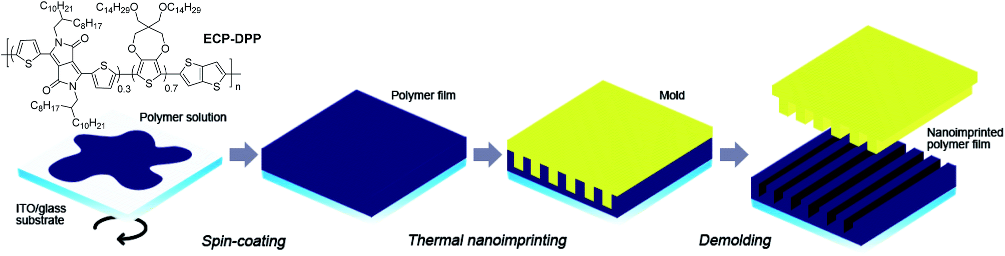 | ||
| Fig. 1 Schematic illustration of the thermal nanoimprinting process for the electrochromic ECP–DPP film. | ||
Thermal nanoimprinting
Electrochromic polymer films with thicknesses of around 135 nm were first spin-coated onto the ITO/glass substrates from a stock solution (10 mg mL−1, 1![[thin space (1/6-em)]](https://www.rsc.org/images/entities/char_2009.gif) :3 v/v chloroform:chlorobenzene) at 300 rpm for 60 second. Polymer edges were removed by swabbing with chloroform using a cotton bud to afford an active area of 1 × 1 cm2. Nano-structuring of the polymer films was subsequently carried out using a thermal nanoimprint lithography process. A silicon mold with line gratings (250 nm width, 250 nm gap and 125 nm depth) was deliberately chosen as it possesses a thickness suitable for the 135 nm spin-coated polymer films. A perfluorodecyltrichlorosilane (FDTS) monolayer was coated on the surface of the mold as an anti-adhesion layer. Prior to the nanoimprinting process, both the polymer film and silicon mold were cleaned using a N2 blower. Following which, the mold was placed on top of the polymer film and placed into the thermal nanoimprinter. The mold and substrate were then heated to a temperature of 120 °C and a constant pressure of 30 and 50 bars were applied onto separate samples for 300 seconds. Subsequently, the system was cooled down to 30 °C and the pressure was released. The mold was then removed to yield the patterned films. A schematic illustration of the procedure is shown in Fig. 1. Herein, the imprinted polymer films that have been subjected to a pressure of 30 and 50 bars during the nanoimprinting process are denoted as ‘NIL-30’ and ‘NIL-50’ respectively. The un-patterned film is referred to as ‘pristine’.
:3 v/v chloroform:chlorobenzene) at 300 rpm for 60 second. Polymer edges were removed by swabbing with chloroform using a cotton bud to afford an active area of 1 × 1 cm2. Nano-structuring of the polymer films was subsequently carried out using a thermal nanoimprint lithography process. A silicon mold with line gratings (250 nm width, 250 nm gap and 125 nm depth) was deliberately chosen as it possesses a thickness suitable for the 135 nm spin-coated polymer films. A perfluorodecyltrichlorosilane (FDTS) monolayer was coated on the surface of the mold as an anti-adhesion layer. Prior to the nanoimprinting process, both the polymer film and silicon mold were cleaned using a N2 blower. Following which, the mold was placed on top of the polymer film and placed into the thermal nanoimprinter. The mold and substrate were then heated to a temperature of 120 °C and a constant pressure of 30 and 50 bars were applied onto separate samples for 300 seconds. Subsequently, the system was cooled down to 30 °C and the pressure was released. The mold was then removed to yield the patterned films. A schematic illustration of the procedure is shown in Fig. 1. Herein, the imprinted polymer films that have been subjected to a pressure of 30 and 50 bars during the nanoimprinting process are denoted as ‘NIL-30’ and ‘NIL-50’ respectively. The un-patterned film is referred to as ‘pristine’.
Device fabrication
On a piece of ITO/glass substrate, parafilm was lined along a 2 × 2 cm2 area to act as both a spacer and barrier layer. Within the blocked-out area, 250 μL of the gel electrolyte (composition: 0.512 g of lithium perchlorate and 2.8 g of poly(methyl methacrylate) (MW = 120000 g mol−1) in 6.65 mL of propylene carbonate and 28 mL of dry acetonitrile (ACN)) was dispensed and left to dry for 5 minutes under ambient conditions. Assembly of the device was carried out on the bench-top by sandwiching both ITO/glass substrates together with the polymer film and gel electrolyte in contact.
Instrumentation
A thermal nanoimprinter (Obducat, Sweden) was employed for thermal nanoimprinting. Atomic force microscopy (AFM) images were captured using a Veeco Dimension 3100 atomic force microscope under the tapping mode. UV-vis-NIR absorption spectra were recorded on a Shimadzu UV-3600 UV-vis-NIR spectrophotometer. An Autolab PGSTAT128N potentiostat was employed for cyclic voltammetry experiments. For the measurements, a three-electrode cell configuration with polymer-coated ITO/glass substrate, Pt wire and Ag wire utilized as the working, counter and pseudo-reference electrodes respectively was used. A 0.1 M LiClO4/ACN electrolyte/solvent couple was used and all measurements were recorded at 50 mV s−1. All electrochromic characterizations were performed in situ, using both the spectrophotometer and potentiostat.Results and discussion
Thin film morphology
The surface morphologies of the nanoimprinted films were probed using AFM and the height images and cross-sectional profiles of both NIL-30 and NIL-50 films are presented in Fig. 2. Thermal nanoimprinting had been successfully carried out on the polymer films and this was confirmed from the presence of periodic one-dimensional nanoscale gratings. The transfer of the patterns from the mold to the polymer film was also achieved at high yields (>95%). The widths of the polymer gratings (represented by the lighter regions in the AFM images) for both NIL-30 and NIL-50 were found to be approximately 275 nm, which is slightly wider than the gaps of the mold (250 nm). The discrepancy is likely due to the limitations in the resolution of the AFM tip.22 For NIL-30 which was imprinted at a lower pressure at 30 bars, the measured depth of the gratings is predictably shallower at 100 nm. In comparison, the gratings of NIL-50 had reached a depth of approximately 130 nm. This is attributed to the increased filling of the patterns under an increased pressure. Nevertheless, the surface profiles achieved with both pressures were similar.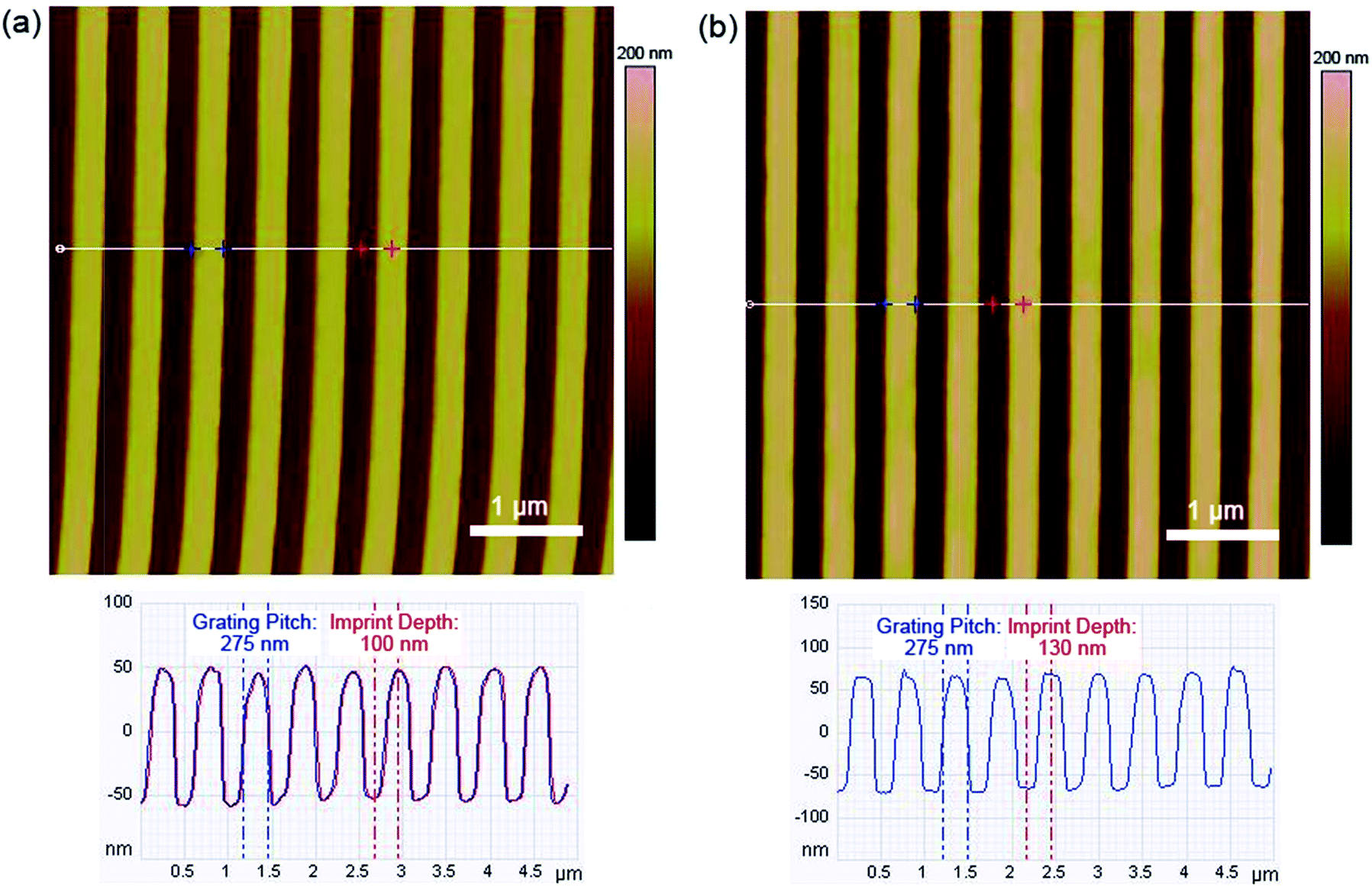 | ||
| Fig. 2 Height images and cross-sectional profiles of nanoimprinted (a) NIL-30 and (b) NIL-50 polymer films. Scan size: 5 × 5 μm. | ||
Optical and electrochemical properties
The spectroscopic properties of the pristine and nanoimprinted films were analysed from their UV-vis absorption behaviours. As illustrated from the absorption spectra in Fig. 3a, the pristine dark magenta polymer film reveals numerous peaks cantered at around 575 and 710 nm. At the lower-energy wavelength region, a shoulder peak (766 nm) also exists. Following the thermal nanoimprinting process, both NIL-30 and NIL-50 films exhibit spectral broadening as well as overall bathochromic shifts in absorption peaks and onset. Moreover, it was also observed that the initial shoulder peak in the pristine film becomes increasingly dominant going from NIL-30 to NIL-50 and the absorption maximum shifts from 766 to 769 and 780 correspondingly. All the above observations indicate the greater π–π stacking behaviour and polymer chain ordering in the nanoimprinted films.17 The alignment of the polymer chains may have been facilitated during the thermal nanoimprinting process as the polymer chains are most likely able to re-orient themselves under elevated temperatures and are constrained into nanoscale structures within the gaps of the mold.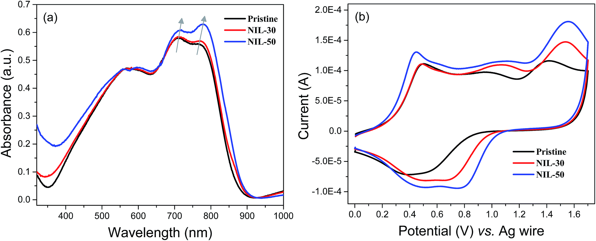 | ||
| Fig. 3 (a) UV-vis absorption spectra and (b) cyclic voltammograms of pristine and nanoimprinted polymer films. | ||
The redox behaviours of the polymer films were subsequently investigated using cyclic voltammetry (CV). For all the pristine and nanoimprinted NIL-30 and NIL-50 films, similar redox profiles were observed. In all cases, the CV curves revealed three pseudo-reversible redox couples upon anodic oxidation (Fig. 3b). Nonetheless, key differences between the pristine and nanoimprinted films are still observed. Firstly, the nanoimprinted NIL-30 and NIL-50 films exhibited a systematic increase in redox activities as indicated by the higher induced currents. Secondly, the potential onsets of the first oxidation peak and reverse reduction peak are found to occur at lower and higher potentials respectively, suggesting the gradual ease of redox reaction in the nanoimprinted polymer films. The enhancement in the redox capability of the nanoimprinted films can most probably be ascribed to the increase in the interfacial area between the electrolyte and accessible redox-active polymers. A summary of the optical and electrochemical properties of the pristine and nanoimprinted polymer films is presented in Table 1.
| λmax (nm) | λonset (nm) | Oxidation potentiala (V) | Reduction potentiala (V) | |||
|---|---|---|---|---|---|---|
| Eox | Eonsetb | Ered | Eonsetc | |||
| a Against pseudo-reference (Ag wire).b First oxidation peak from neutral to positively-charged state.c First reduction peak from positive-charged to neutral state. | ||||||
| Pristine | 575, 710, 766 (sh) | 871 | 0.50, 0.96, 1.41 | 0.30 | 0.38, 0.55 | 0.83 |
| NIL-30 | 575, 712, 770 | 876 | 0.49, 1.06, 1.53 | 0.29 | 0.49, 0.67 | 0.95 |
| NIL-50 | 575, 716, 779 | 886 | 0.44, 1.06, 1.56 | 0.26 | 0.51, 0.77 | 1.01 |
Electrochromic performance
The electrochromic performances of the pristine and nanoimprinted polymer films were investigated in the form of absorption/transmission type devices. Between the neutral and oxidized states, the devices reveal dark magenta-to-transmissive grey electrochromic switching. An illustration of the colour changes using the NIL-50 electrochromic device (ECD) is shown in Fig. 4a. Interestingly, unlike the pristine un-patterned polymer film which shows an identical hue regardless of the viewing angle, the nanoimprinted films are able to reveal different hues under different viewing angles due to the ability of the nanogratings to diffract ambient white light (Fig. 4b). This property could potentially give rise to numerous interesting applications,14,15 but it is beyond the scope of this work. | ||
| Fig. 4 Photographs of (a) NIL-50 ECD in its neutral (0.0 V) and oxidized (1.6 V) states, and (b) NIL-50 film displaying different hues under different viewing angles. | ||
The electrochromic parameters of the ECDs such as the optical contrasts, switching speeds and coloration efficiencies were probed at 720 nm and the effect of nano-structuring of the polymer film on its performance is examined. For the experiments, oxidative and reductive biases of +1.6 and −1.6 V were applied to the devices while the changes in transmittance were monitored over time. For each of the samples, three trials were carried out. Fig. 5 depicts the switching cycles for the pristine and nanoimprinted ECDs. The maximum optical contrasts attained for the nanoimprinted devices were found to be slightly improved. From a value of around 33% for the pristine device, the observed contrast slightly increases to 34% and 36% in NIL-30 and NIL-50 respectively. Other than the magnitude of colour contrast, the response times (calculated as the time required for the device to switch to 95% of the optical contrast) for the nanoimprinted devices are also determined to be faster than the pristine device. For instance, between the pristine and NIL-30 devices, the latter reveal bleaching and coloration speeds that are approximately 6–8% faster. Similarly for the NIL-50 devices, improvements by approximately 20 and 7% respectively were recorded against the pristine ECDs. More prominently, the coloration efficiencies were observed to be larger for both the nanoimprinted devices, implying lower power consumptions and greater energy savings. The average value increases from 211 (pristine) to 247 (NIL-30) and finally to 254 cm2 C−1 (NIL-50). A graphical summary of the electrochromic performance of the various ECDs is shown in Fig. 6 while the detailed experimental data are presented in Table 2.
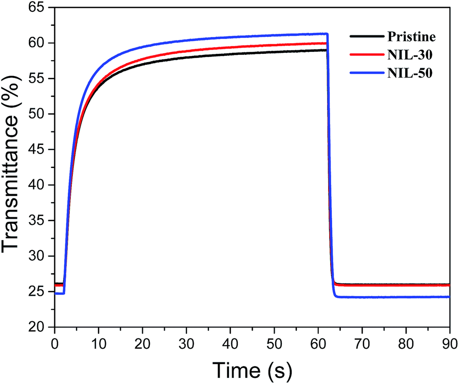 | ||
| Fig. 5 Transmittance-time profiles of pristine and nanoimprinted ECDs cycled between +1.6 and −1.6 V at 720 nm. | ||
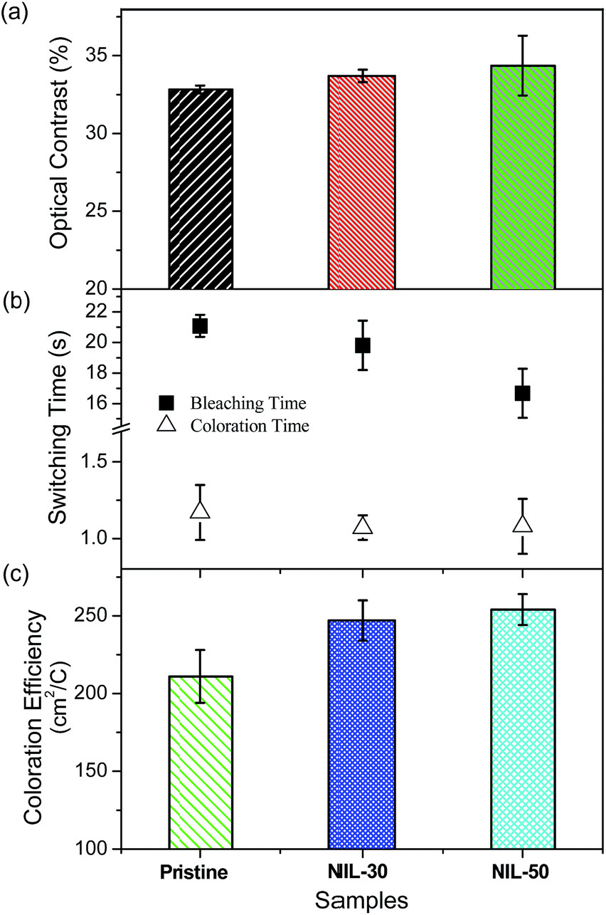 | ||
| Fig. 6 Graphical summary of the electrochromic performance ((a) optical contrast, (b) switching time and (c) coloration efficiency) of pristine and nanoimprinted ECDs probed at 720 nm. | ||
| Exposed surface areab (cm2) | Optical contrast (%) | Bleaching time (s) | Coloration time (s) | Coloration efficiency (cm2 C−1) | |
|---|---|---|---|---|---|
| a All measurements are carried out at 720 nm.b Exposed surface area is estimated based on the number of and depth of nanogratings in the polymer films within the 1 × 1 cm2 active area. | |||||
| Pristine | 1.00 | 32.8 ± 0.3 | 21.1 ± 0.7 | 1.17 ± 0.18 | 211 ± 17 |
| NIL-30 | 1.18 | 33.7 ± 0.4 | 19.8 ± 1.6 | 1.07 ± 0.08 | 247 ± 13 |
| NIL-50 | 1.23 | 34.4 ± 1.9 | 16.7 ± 1.6 | 1.08 ± 0.18 | 254 ± 10 |
The enhancement in the optical contrast of the ECDs following nano-structuring can most likely be accounted for by the increased amount of accessible chromophoric polymer sites that can undergo the redox reaction under the potential bias. This is supported by the observed differences between the performance of NIL-50 and NIL-30, in which the former possesses a larger exposed surface area (∼1.23 cm2 vs. ∼1.18 cm2) due to the higher depth of the nanogratings. Nonetheless, a linear relationship between the surface area of the polymer film and optical contrast is not observed. By increasing the interfacial area between the electrochromic polymer and electrolyte, the ion diffusion distance is also speculated to be shortened. This is likely to enable more facile movement of the charge-balancing counter-ions towards the charged polymeric species during the redox process, leading to more rapid electrochromic switching. Besides one-dimensional line gratings, other nanoscale geometrical structures with even higher aspect ratios are also expected to yield similar and improved benefits.
Conclusions
Ordered nanostructured line gratings were successfully patterned onto the electrochromic polymer films through an easy and quick thermal nanoimprinting process. The approach was observed to induce closely-packed and aligned polymer chains, as well as to enhance the ease of redox activity of the polymer film through an increase in the exposed interfacial surface area. When assembled into electrochromic devices, the nanoimprinted polymer films were found to exhibit superior performances in optical contrast, switching speeds and coloration efficiency compared to the pristine, un-patterned counterpart. Experimental findings also appear to reveal a direct correlation between the polymer-electrolyte interfacial area and electrochromic performance, albeit not linearly. It is envisaged that morphology control and optimization of the polymer films could be among the effective strategies to enhance the performance of electrochromic devices.Conflicts of interest
There are no conflicts to declare.Acknowledgements
This research was supported by the Agency for Science, Technology and Research (A*STAR) and the Ministry of National Development (MND) Green Building Joint Grant (No. 1321760011) and also the Nanoimprint Foundry Grant (No. 1325307091).Notes and references
- H. Shin, S. Seo, C. Park, J. Na, M. Han and E. Kim, Energy Environ. Sci., 2016, 9, 117–122 CAS
.
- J. Remmele, D. E. Shen, T. Mustonen and N. Fruehauf, ACS Appl. Mater. Interfaces, 2015, 7, 12001–12008 CAS
- A. M. Österholm, D. E. Shen, J. A. Kerszulis, R. H. Bulloch, M. Kuepfert, A. L. Dyer and J. R. Reynolds, ACS Appl. Mater. Interfaces, 2015, 7, 1413–1421 Search PubMed
- P. Chandrasekhar, B. J. Zay, C. Cai, Y. Chai and D. Lawrence, J. Appl. Polym. Sci., 2014, 131, 41043 Search PubMed
- W. M. Kline, R. G. Lorenzini and G. A. Sotzing, Color. Technol., 2014, 130, 73–80 CAS
- J. Padilla, A. M. Österholm, A. L. Dyer and J. R. Reynolds, Sol. Energy Mater. Sol. Cells, 2015, 140, 54–60 CrossRef CAS
- A. Kumar, C. Asemota, J. Padilla, M. Invernale, T. F. Otero and G. A. Sotzing, J. Phys.: Conf. Ser., 2008, 127, 012014 CrossRef
- M. Cui, W. S. Ng, X. Wang, P. Darmawan and P. S. Lee, Adv. Funct. Mater., 2015, 25, 401–408 CrossRef CAS
- D. M. DeLongchamp, M. Kastantin and P. T. Hammond, Chem. Mater., 2003, 15, 1575–1586 CrossRef CAS
- D. Ge, L. Yang, Z. Tong, Y. Ding, W. Xin, J. Zhao and Y. Li, Electrochim. Acta, 2013, 104, 191–197 CrossRef CAS
- H.-Y. Wei, Y.-S. Hsiao, J.-H. Huang, C.-Y. Hsu, F.-C. Chang, P. Chen, K.-C. Ho and C.-W. Chu, RSC Adv., 2012, 2, 4746–4753 RSC
- J. Jensen, A. L. Dyer, D. E. Shen, F. C. Krebs and J. R. Reynolds, Adv. Funct. Mater., 2013, 23, 3728–3737 CrossRef CAS
- A. Leliège, S. Barik and W. G. Skene, ACS Appl. Mater. Interfaces, 2014, 6, 6920–6929 Search PubMed
- T. Bhuvana, B. Kim, X. Yang, H. Shin and E. Kim, Nanoscale, 2012, 4, 3679–3686 RSC
- T. Bhuvana, B. Kim, X. Yang, H. Shin and E. Kim, Angew. Chem., Int. Ed., 2013, 52, 1180–1184 CrossRef CAS PubMed
- S. Admassie and O. Inganäs, J. Electrochem. Soc., 2004, 151, H153–H157 CrossRef CAS
- Y. Kim, Y. Kim, S. Kim and E. Kim, ACS Nano, 2010, 4, 5277–5284 CrossRef CAS PubMed
- H. Benten, D. Mori, H. Ohkita and S. Ito, J. Mater. Chem. A, 2016, 4, 5340–5365 CAS
- J. Liu, T.-F. Guo and Y. Yang, J. Appl. Phys., 2002, 91, 1595–1600 CrossRef CAS
- J. Choi, A. Kumar and G. A. Sotzing, J. Macromol. Sci., Part A: Pure Appl.Chem., 2007, 44, 1305–1309 CrossRef CAS
- W. T. Neo, Z. Shi, C. M. Cho, S.-J. Chua and J. Xu, ChemPlusChem, 2015, 80, 1298–1305 CrossRef CAS
- D. Cheyns, K. Vasseur, C. Rolin, J. Genoe, J. Poortmans and P. Heremans, Nanotechnology, 2008, 19, 424016 CrossRef CAS PubMed
| This journal is © The Royal Society of Chemistry 2017 |