
 Open Access Article
 This Open Access Article is licensed under a
 Creative Commons Attribution 3.0 Unported Licence
Strain-induced thermoelectric performance enhancement of monolayer ZrSe2
Dan Qin ab,
Xu-Jin Gea,
Guang-qian Dinga,
Guo-ying Gaoa and
Jing-Tao Lü*a
ab,
Xu-Jin Gea,
Guang-qian Dinga,
Guo-ying Gaoa and
Jing-Tao Lü*a
aSchool of Physics, Huazhong University of Science and Technology, 430074 Wuhan, P. R. China. E-mail: qindan_ok@163.com; guoying_gao@mail.hust.edu.cn; jtlu@hust.edu.cn
bPhysics Department, Binzhou Medical University, 264003 Yantai, Shangdong, P. R. China
First published on 6th October 2017
Abstract
Monolayer ZrSe2 was previously predicted to be one kind of excellent thermoelectric material due to its low lattice thermal conductivity. Motivated by the recent proposal of enhancing thermoelectric performance via strain-induced electronic band degeneracy, we have performed first-principles calculations on the effect of biaxial tensile strain on the thermoelectric properties of monolayer ZrSe2 combined with Boltzmann transport theory and deformation potential theory. The theoretical results demonstrate that the band degeneracy reaches its maximum at 7.5% strain, resulting in an increase of the Seebeck coefficient and, at the same time, a decrease of the lattice thermal conductivity. At this optimal strain, a two-fold increase of the figure of merit is obtained for an n-doped ZrSe2 monolayer at room temperature. Moreover, the figures of merit for p- and n-type doping are much more balanced in the strain case compared with the unstrained one.
Introduction
As a potentially important technology for the conversion of heat flow to electrical work and vice versa, thermoelectrics (TEs) have attracted more and more attention over the past several decades.1 The thermoelectric performance is usually characterized in terms of the dimensionless figure of merit ZT, which is given by ZT = S2σT/(kL + ke). Here, S is the thermopower or Seebeck coefficient, σ the electrical conductivity, T the absolute temperature, and kL and ke are the thermal conductivities contributed by a phonon and an electron, respectively.2 Therefore, large values of ZT demand high S and high σ, as well as low thermal conductivity (kL + ke). Since an increase in S normally implies a decrease in σ, while an increase in σ implies an increase in ke as given by the Wiedemann–Franz law, it is hard work to increase ZT in typical thermoelectric materials. In the past decade, a lot of effort has been focused on low-dimensional systems for their unique electronic and phonon transport behaviors.3–11Thermoelectric transport performance can benefit from several advantages of low-dimensional materials, including: (1) sharp changes of the density of states near the Fermi energy EF, resulting in an increase in the Seebeck coefficient; (2) opportunities to exploit the anisotropic Fermi surfaces in multi-valley semiconductors; (3) opportunities to increase the boundary scattering of phonons at interfaces, resulting in a decrease in lattice thermal conductivity. In recent years, two-dimensional (2D) materials have been widely investigated as thermoelectric materials, such as graphene,12 boron-nitride,13 and black phosphorus.14 Particularly, the class of transition-metal dichalcogenides (TMDCs) MX2 (M = Mo, W; X = S, Se)15–19 has received great interest due to their unique properties being superior to those of their corresponding bulk states. Typical monolayers of MoS2 (ref. 18) and WSe2 (ref. 19) exhibit ZT values of 0.11 and 0.7 at high temperature. Such low ZT is mainly caused by high kL, which is as large as 100 W m−1 K−1 for MoS2 at room temperature and larger than 40 W m−1 K−1 for MoSe2. It is worth noting that all of the above explored monolayer TMDCs have hexagonal 2H-type crystal structure. Another trigonal 1T-CdI2 type of TMDC with M = Zr and Hf has recently been predicted to have much lower kL,20 with 1.2 W m−1 K−1 for ZrSe2 and 1.8 W m−1 K−1 for HfSe2 at 300 K. Similar behavior was also found in CdI2 type monolayer ZrS2.21 These results indicate that monolayer TMDCs with CdI2 type structure may have better thermoelectric performance due to their much lower kL than those of MoS2 type monolayers.
Recently, the thermoelectric performance of CdI2 type monolayer HfS2 was found to be further enhanced through strain-induced electronic band degeneracy.22 It is known that the electronic transport performance depends primarily on  ,23–25 where NV is the valley degeneracy, μ is the carrier mobility,
  is the average (single valley) density of states effective mass of the degenerate valleys, and me is the electron mass. It has been demonstrated that a large valley degeneracy is good for thermoelectric materials,26 and can be realized when multiple bands have band extrema around the same energy (orbital degeneracy) or when multiple carrier pockets of one band in the Brillouin zone are degenerate (valley degeneracy).27 As reported in previous works, strain engineering is an effective approach to tune the electronic band to achieve degeneracy.21,22,28–31
Consequently, on the one hand, the strain-induced band degeneracy increases the electronic transport performance, while on the other hand, the distortion of phonon dispersion may lower kL, both leading to an enhanced ZT. According to the most recent work, among the CdI2 type monolayers of ZrX2 and HfX2 (X = S, Se), ZrSe2 shows the lowest lattice thermal conductivity.20 Moreover, the monolayers of ZrX2 and HfX2 have similar electronic band structures and can stand 10% biaxial tensile strain.32 Motivated by these results, we apply this kind of thermoelectric optimization to a monolayer of ZrSe2. In this paper, combining first-principles calculations with the Boltzmann transport equation (BTE), we perform a comprehensive study of the electronic band structures, phonon dispersions and thermoelectric properties of monolayer ZrSe2 and compare the results to those of monolayer ZrS2.
Computational details
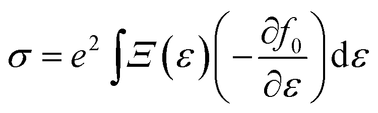
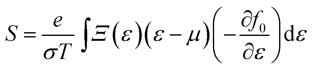
We first carried out first-principles electronic structure calculations using the Vienna ab initio simulation package (VASP).33 The PBE form of the generalized gradient approximation34 was used for the exchange–correlation functional. The plane-wave cutoff energy was set to 600 eV and the Monkhorst–Pack k mesh is 15 × 15 × 1. Geometrical structures were relaxed until the force on each atom was less than 0.001 eV Å−1. In order to avoid interaction with periodic images, 15 Å of vacuum was included in the direction perpendicular to the 2D plane.It should be pointed out that the traditional GGA functional tends to underestimate the energy band gap, which is important for thermoelectric performance.35 Whereas, the hybrid functional tends to overestimate the band gaps of monolayer TMDCs according to previous calculations.32 Here, unless specified, we performed electronic structure calculations employing the full-potential WIEN2K code36 without considering the hybrid functional after determining the equilibrium structure. We have checked that using the Heyd–Scuseria–Ernzerhof (HSE) functional37 has little effect on the power factor. In these calculations we used RMT × Kmax = 8.0, a muffin-tin radius of 2.0 a.u. for both the Zr and Se atoms, and a 19 × 19 × 1 k-point Monkhorst–Pack mesh. Due to Zr and Se being 4d and 3d elements, respectively, we did not consider the spin–orbit coupling in all calculations. Based on the electronic structure calculations, a more dense nonshifted 87 × 87 × 1 k-point Monkhorst–Pack mesh was used for the transport calculations to guarantee convergence and to obtain accurate carrier group velocities. The electrical conductivity and Seebeck coefficient are calculated from 38
 | (1) |
 | (2) |
 , in which
  is the αth component of the group velocity of the carriers with wave vector k.
Thermoelectric transport properties were calculated by solving the Boltzmann transport equations within the rigid band approximation and constant relaxation-time approximation (RBA and CRTA) as implemented in the BoltzTraP code.38 The CRTA has been successfully applied to many thermoelectric materials.39–41 The influence of doping is considered in the rigid band model, which assumes that light doping does not change the shape of the band structure, but only shifts the Fermi energy. By using the CRTA, τ is exactly cancelled out in eqn (2). Thus, from the above calculations we can obtain the Seebeck coefficient S and the electrical conductivity over relaxation time as well (σ/τ). The electronic thermal conductivity ke is calculated using the Wiedemann–Franz law, ke = LσT, where L is the Lorenz number. In this work we use L = 1.5 × 10⁻⁸ J2 K−2 C−2.42 We have also calculated the lattice thermal conductivity kL and related phonon quantities. The phonon frequencies were calculated using density functional perturbation theory (DFPT) as implemented in the VASP code.33 The phonon dispersion and eigenmodes were calculated by diagonalizing the dynamical matrix, which is constructed from harmonic interatomic force constants (IFCs) using the Phonopy code.43 In those calculations, the second order harmonic and third order anharmonic IFCs were calculated using a 5 × 5 × 1 supercell with 2 × 2 × 1 Monkhorst–Pack k meshes and a 4 × 4 × 1 supercell with Γ point, respectively. We then solved the phonon Boltzmann transport equation based on an adaptive smearing approach to the conservation of energy44 and with an iterative solution method,45 as implemented in ShengBTE.46
Results and discussion
Now we discuss the geometric and electronic structure of the ZrSe2 monolayer. For intrinsic monolayer ZrSe2, we have obtained the lattice parameters of a = b = 3.79 Å, which are very close to its bulk parameters and agree well with the values from previous literature.47 The top and side views of monolayer ZrSe2 are shown in Fig. 1(a) and (b), respectively. Based on the optimized structure, we calculated the electronic structure with the Brillouin zone path along Γ–M–K–Γ as shown in Fig. 1(c). The calculated electronic band structure of the ZrSe2 monolayer is shown in Fig. 2(a), which indicates that the ZrSe2 monolayer is an indirect band gap semiconductor, with the valence band maximum (VBM) and conduction band minimum (CBM) located at the Γ and M points, respectively. The band gap is calculated to be 0.47 eV, which shows good agreement with previous calculations.47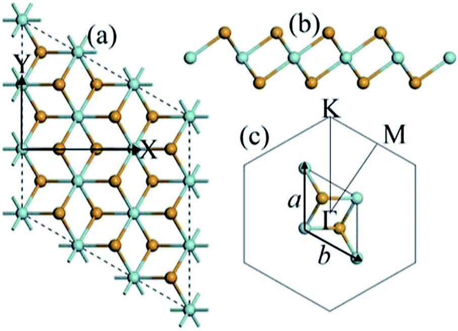 | ||
| Fig. 1 (a) Top and (b) side views of monolayer ZrSe2 in CdI2 type structure, where the green and yellow balls represent the Zr and Se atoms, respectively. X and Y denote the armchair and zigzag directions of the monolayer, respectively. (c) The unit cell and corresponding Brillouin zone path with high-symmetry points at Γ(0,0,0), M(0.5,0,0) and K(1/3,1/3,0). | ||
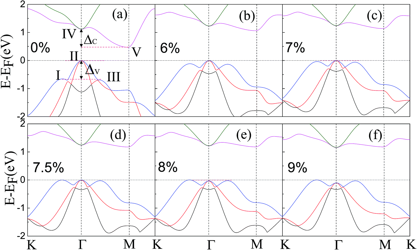 | ||
| Fig. 2 Band structures of the ZrSe2 monolayer along high-symmetry k-points under different biaxial strains of (a) 0%, (b) 6%, (c) 7%, (d) 7.5%, (e) 8%, and (f) 9%. The three valence band valleys near the Fermi level are denoted by I, II, and III, respectively. The two conduction band valleys near the Fermi level are denoted by IV and V, respectively. ΔV (ΔC) represents the energy difference between I and II (IV and V). | ||
In order to increase the degenerate carrier pockets near the Fermi level, we applied a series of in-plane biaxial tensile strains to the ZrSe2 monolayer, which are defined as ε = (a − a0)/a0 × 100%. Here a0 is an unstrained cell parameter, and a is a strained cell parameter. Tensile strains ranging from 0 to 9% were considered and only the results of 6%, 7%, 7.5%, 8% and 9% tensile strain are given as representative cases; the corresponding band structures are shown in Fig. 2(a), (b), (c), (d), (e) and (f), respectively. The DFT calculated band gaps increase from 0.47 eV at zero strain to 1.18 eV when the biaxial tensile strain is beyond 7.5%, as shown in Fig. 3. As can be seen in Fig. 2(a), the valence band valleys near the Fermi level are denoted by I, II and III, where the extrema of valleys I and III are about 0.6 eV below valley II. The two conduction band valleys near the Fermi level are denoted by IV and V, with two valleys being degenerate at the II and IV points. The energy difference between valley I and II (IV and V) is denoted as ΔV (ΔC), namely ΔV = EII − EI and ΔC = EIV − EV. It is suggested that the bands may be regarded as effectively converged when their energy separation is small compared with kBT, where kB is the Boltzmann constant.26 Thus it is clear that a high valley degeneracy in the Brillouin zone can be obtained by minimizing the values of ΔV and/or ΔC. At zero strain, the extreme of valley II is the highest among the three valence band valleys, while the V valley is the lowest among the two conduction valleys. When tensile strain is applied, the extremes of these valence band valleys gradually get closer to each other in energy as the strain increases, resulting in a decrease of ΔV as shown in Fig. 2. At a strain of 7.5%, the three valleys are nearly degenerate. As a consequence, the degeneracy of the hole carrier pockets reaches the maximum. On further increasing the biaxial strain, the extreme of valley II shifts down and thus the degeneracy level is reduced, as displayed in Fig. 2. For the conduction band, as demonstrated in Fig. 2, the band valley V is elevated gradually following the increasing strain, leading to a decrease of ΔC. The increase of the band valley degeneracy is beneficial to the thermoelectric performance. We thus expect an enhanced thermoelectric performance for monolayer ZrSe2 via this strain-induced valley degeneracy. Next we will discuss the electronic properties of ZrSe2 under different tensile strains.
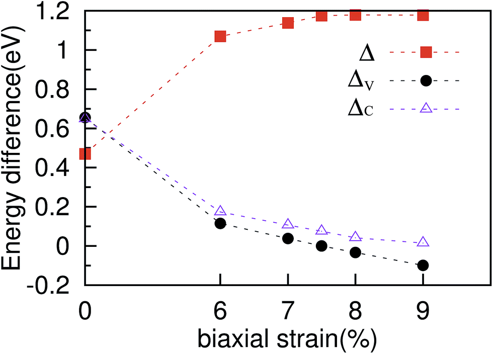 | ||
| Fig. 3 Calculated electronic band gaps (Δ) and energy difference between the valence and conduction band valleys (ΔV and ΔC) as a function of the applied biaxial tensile strain ranging from 0 to 9%. | ||
Electronic transport properties
In this part, we analyse the electronic properties of the ZrSe2 monolayer without and with biaxial strain. We have performed calculations of the electronic transport coefficients by using the semiclassical Boltzmann theory.The left (right) panels in Fig. 4 show the electronic transport coefficients with respect to the biaxial tensile strain of 0%, 6%, 7.5% and 9% as a function of the hole (electron) concentration at T = 300 K. As can be seen in Fig. 4(a) and (b), the electrical conductivity σ/τ increases with increasing carrier concentration and decreases with increasing biaxial tensile strains, which is because of the increase of the band gap as shown in Fig. 3. Such an influence on conductivity with the applied strain will exert a negative effect on the thermoelectric properties. However, the calculated absolute values of the Seebeck coefficients at 300 K (see Fig. 4(c) and (d)) increase with the increase of the strain initially, then reach their maxima at a strain of 7.5%, and then slightly decrease when the strain is further increased. It is important to note that the Seebeck coefficients for both n- and p-type doped ZrSe2 monolayers at a biaxial tensile strain of 7.5% are quite enlarged at room temperature, reaching a peak value of 725 μV K−1 at a hole concentration around 1011 cm−2. These enhanced values of S for a monolayer compare favorably with those reported for optimized MoS2![[thin space (1/6-em)]](https://www.rsc.org/images/entities/char_2009.gif) 18 and HfO2.48 The trend of the Seebeck coefficient as a function of the strain is almost in accordance with the difference energy of ΔV (see Fig. 3), that is, the enhanced Seebeck coefficient is mainly due to the increased degeneracy of the band valley. Fig. 4(e) and (f) show the power factor (PF) S2σ/τ under different strains at 300 K dependent on the carrier concentration for the p- and n-type carriers, respectively. The results show that the power factor for n-type doping is much larger than that for the p-type doping at zero strain, which is due to the larger Seebeck coefficient for n-type doping. In addition, for either p- or n-type doping, the peak value of the PF initially increases with increasing strain, then reaches the maximum at a strain of 7.5%, and then declines slightly on increasing the strain further. It is worth noting that the trend of the PF with respect to the strain is the same as that of the Seebeck coefficient, indicating that the negative effect of the strain on the electrical conductivity is counteracted by the increase of the Seebeck coefficient.
18 and HfO2.48 The trend of the Seebeck coefficient as a function of the strain is almost in accordance with the difference energy of ΔV (see Fig. 3), that is, the enhanced Seebeck coefficient is mainly due to the increased degeneracy of the band valley. Fig. 4(e) and (f) show the power factor (PF) S2σ/τ under different strains at 300 K dependent on the carrier concentration for the p- and n-type carriers, respectively. The results show that the power factor for n-type doping is much larger than that for the p-type doping at zero strain, which is due to the larger Seebeck coefficient for n-type doping. In addition, for either p- or n-type doping, the peak value of the PF initially increases with increasing strain, then reaches the maximum at a strain of 7.5%, and then declines slightly on increasing the strain further. It is worth noting that the trend of the PF with respect to the strain is the same as that of the Seebeck coefficient, indicating that the negative effect of the strain on the electrical conductivity is counteracted by the increase of the Seebeck coefficient.
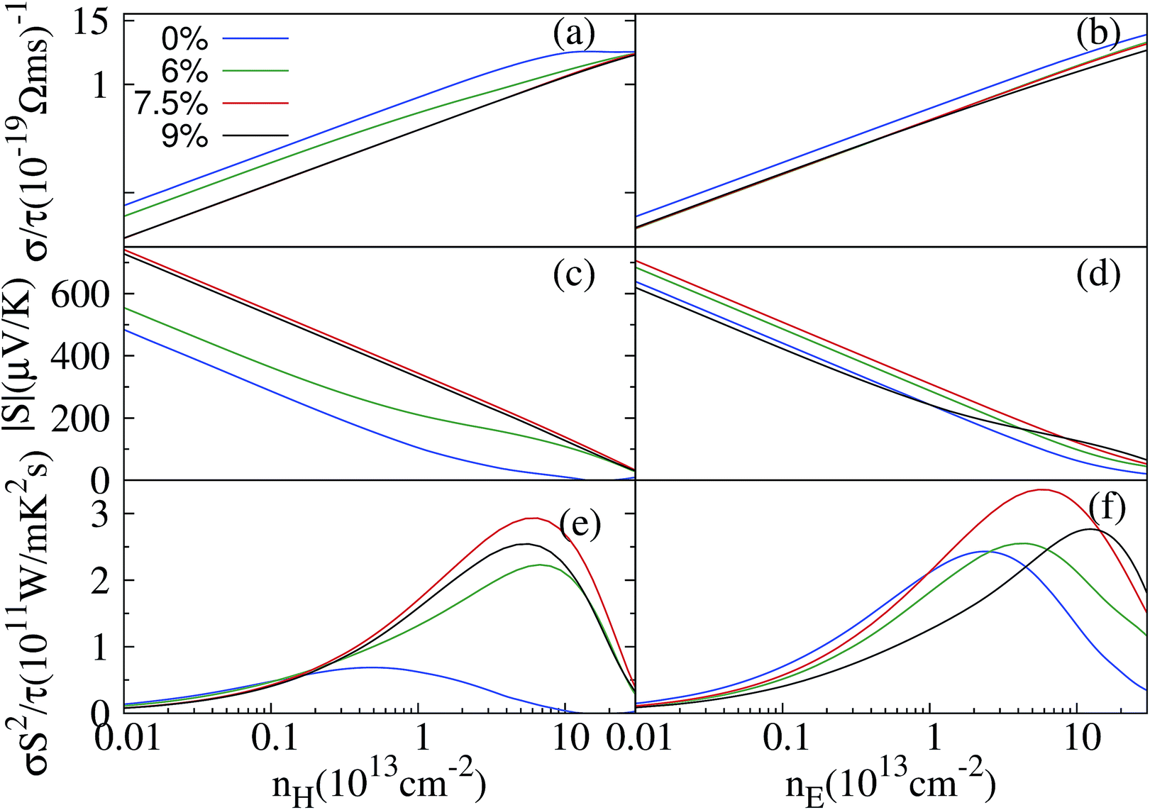 | ||
| Fig. 4 Calculated transport coefficients σ/τ (a and b), S (c and d), and σ/S2τ (e and f) under different biaxial strains of 6%, 7.5% and 9% as a function of carrier concentration. The left and right panels correspond to p- and n-type doping at room temperature, respectively. | ||
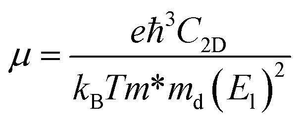
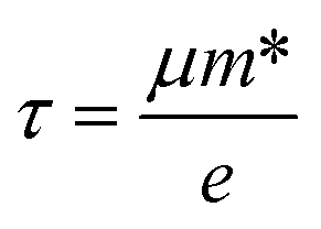
Within the relaxation time approximation, the Seebeck coefficient can be calculated independently of the relaxation time τ, but evaluation of the electrical conductivity (σ) requires knowledge of τ, which is obtained from either fitting of the experiments or theoretical estimation. There are different types of carrier scattering processes that need to be considered in estimating the relaxation time. Here we take into account only the intrinsic scattering mechanism, namely, the interaction of electrons with acoustic phonons. We use the Bardeen–Shockley deformation potential approach for 2D materials,49,50 where the atomic displacement associated with a long-wavelength acoustic phonon leads to a deformation of the crystal, and in turn, to a shift of the electronic energy dispersion. Followed by the deformation potential theory, the carrier mobility and the relaxation time τ in 2D materials are calculated using the equations
 | (3) |
 | (4) |
 , El is the deformation potential constant and C2D is the effective elastic modulus. The calculated results of these parameters are listed in Table 1. We now turn our attention to the effective mass and carrier mobility, as shown in Table 1. Under unstrained conditions, the effective mass is almost isotropic for the hole due to the isotropic band dispersion near the VBM. For the electron, the effective mass is highly anisotropic, and is much higher along the armchair direction (2.32me) than along the zigzag direction (0.34me), since the conduction band dispersion near the Fermi level along the M–K direction (zigzag direction in real space) is much steeper than that along the M–Γ direction (armchair direction in real space). As we know, the small effective masses of the carriers may lead to a high carrier mobility. Using the deformation potential theory, the charge carrier mobility can be predicted from the carrier effective mass, deformation potential constant and effective 2D elastic modulus, as listed in Table 1. When a biaxial strain of 7.5% is applied, the effective mass for an electron increases in the zigzag direction, but decreases significantly in the armchair direction. It can be seen from the results that the carrier mobility is reduced under strain, resulting in the decrease of the electrical conductivity (σ/τ). This is in agreement with the electronic transport calculation as shown in Fig. 4(a) and (b). Since the difference of carrier mobility is reduced, the power factors for p- and n-type have just little differences (see Fig. 4(e) and (f)). Based on eqn (3) and (4), the relaxation time τ can be calculated and, as shown in Table 1, it is almost isotropic in different directions. Therefore, we will use the averaged τ of the armchair and zigzag directions to evaluate the thermoelectric performance later.
| Direction | Deformation | Carriers | m* (me) | md (me) | D (eV Å−2) | El (eV) | μ (cm2 V−1 s−1) | τ (10−13 s) |
|---|---|---|---|---|---|---|---|---|
| Zigzag | Unstrained | e | 0.34 | 0.89 | 5.61 | −2.03 | 1539.51 | 2.98 |
| h | −0.38 | 0.37 | 5.61 | −3.33 | 1231.31 | 2.66 | ||
| Strained | e | 1.17 | 0.76 | 5.61 | −2.90 | 256.71 | 1.71 | |
| h | −0.42 | 0.41 | 5.61 | −4.31 | 600.14 | 1.44 | ||
| Armchair | Unstrained | e | 2.32 | 0.89 | 5.60 | −2.20 | 192.10 | 2.54 |
| h | −0.37 | 0.37 | 5.60 | −3.29 | 1295.53 | 2.73 | ||
| Strained | e | 0.50 | 0.76 | 5.60 | −2.56 | 770.87 | 2.19 | |
| h | −0.40 | 0.41 | 5.60 | −4.19 | 666.76 | 1.52 |
Lattice thermal conductivity
We now investigate the influence of biaxial strain on phonon dispersions and thermal conductivity. The phonon dispersions of the ZrSe2 monolayer under no strain and when under 7.5% biaxial tensile strain are displayed in Fig. 5(a) and denoted by a black solid line and red dashed line, respectively. No imaginary frequency is observed, indicating kinetic stability. By means of the phonon Boltzmann transport equation and DFT, the lattice thermal conductivity is calculated, as depicted in Fig. 5(b). It can be seen from the figure that due to the effective strain, the phonon thermal conductivity kL has been successfully reduced. The reduced lattice thermal conductivity is beneficial to thermoelectric transport, which can also be achieved in Mg2Sn using strain.51 Moreover, with the increasing temperature kL decreases following a T−1 dependence either under no strain or under strain, as presented by the fitted lines in the figure. This suggests that Umklapp phonon scattering dominates three-phonon interactions.52 We will refer to the corresponding phonon dispersions (see Fig. 5(a)) to investigate the origin of the reduction in the thermal conductivity by applying strain. Since the heat transfer is mainly contributed to by the acoustic modes, we will focus on the three phonon models of the transverse (ZA and TA) and longitudinal acoustic (LA) modes. From Fig. 5(a), two out of three of the acoustic branches correspond to vibration within the plane of the transverse and longitudinal acoustic modes (TA and LA) at 7.5% and are actually softer than those at 0 strain along the whole high symmetry line in the Brillouin zone. For example, the boundary frequencies of TA (LA) along Γ–K and Γ–M decline from 3.67 (3.67) and 1.86 (2.79) THz to 2.92 (2.92) and 1.52 (2.27) THz, respectively, which has been proven to be beneficial to reduce the lattice thermal conductivity as reported in previous works.21,53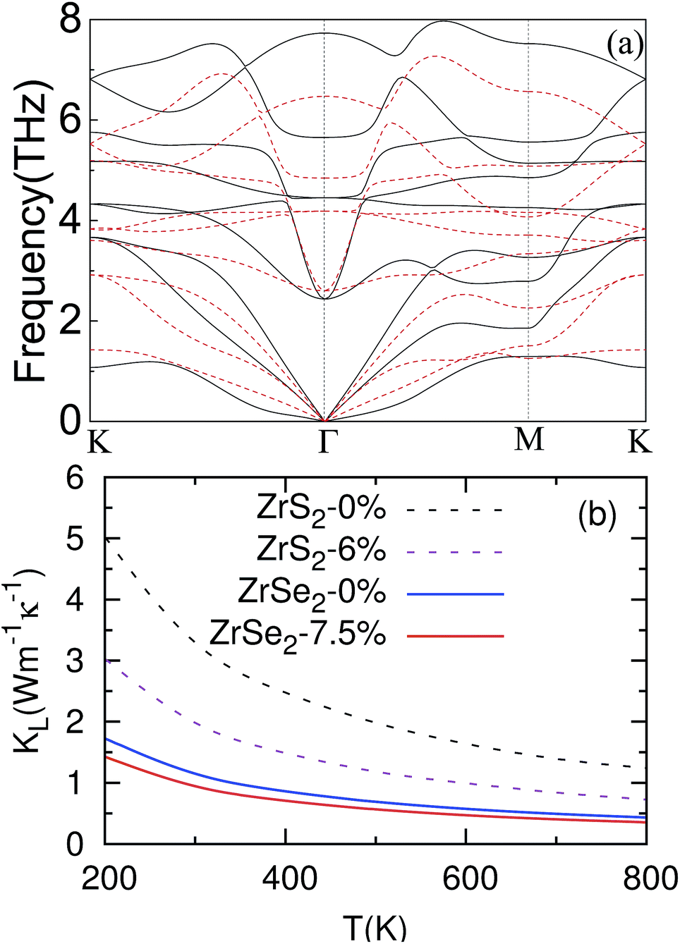 | ||
| Fig. 5 (a) Calculated phonon dispersion under 0% (denoted by the black solid line) and 7.5% (denoted by the dashed line) strain. (b) Lattice thermal conductivity comparison of ZrS2 (under 0% and 6% strain) and ZrSe2 (under 0% and 7.5% strain) monolayers from 200 K to 800 K. | ||
To make a direct comparison, we have plotted the lattice thermal conductivities of ZrSe2 and ZrS2 (ref. 21) monolayers under no strain and under their optimal strains in Fig. 5(b). Obviously, for both ZrSe2 and ZrS2 monolayers, the lattice thermal conductivity kL decreases with the increasing temperature. Moreover, the kL for ZrSe2 is always much lower than that of ZrS2 within the temperature range we investigated. Particularly, the kL values at 300 K are 3.29 (1.99) W m−1 K−1 for ZrS2 and 1.15 (0.94) W m−1 K−1 for ZrSe2 under no strain (under optimal strain), which implies that ZrSe2 may be preferable to ZrS2 in thermoelectric applications.
Figure of merit
Now we are in a position to evaluate the thermoelectric figure of merit ZT. The doping-dependent ZT for unstrained and 7.5% strained ZrSe2 monolayers at room temperature are depicted in Fig. 6. For the unstrained case, the maximum ZT value of the n-type doped system is 4.26, which is about 2 times larger than that of the p-type system. When a strain of 7.5% is applied, the values of ZT for the n-type and p-type doped systems increase to 4.58 and 3.84, respectively. The enhanced ZT is mainly due to the increased power factor S2σ as well as the decreased lattice thermal conductivity kL when under strain. Furthermore, the strain engineering has induced much more balanced ZT values for n- and p-type, which are very desirable for the fabrication of thermoelectric moduli.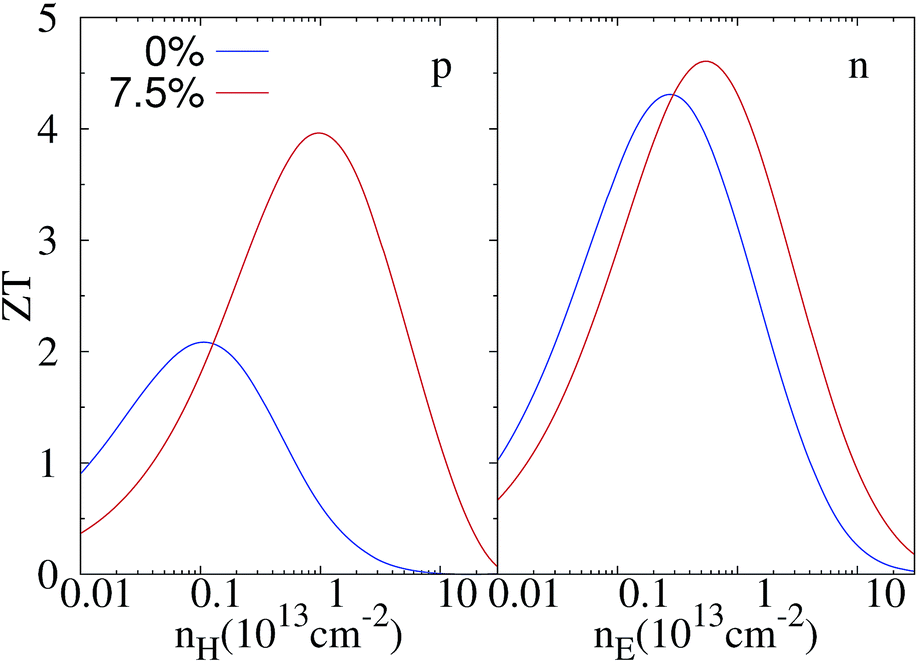 | ||
| Fig. 6 Estimated figure of merit of monolayer ZrSe2 for both p- (left panel) and n-type (right panel) under 0% and 7.5% strain at 300 K. | ||
In addition, we should mention some facts as follows: (1) to date, developing an effective method to apply tunable strain in 2D layers such as MoS2 is highly desirable. Based on the wealth of theoretical studies on band engineering using strain and some strategies for exploring strain on 2D materials in recent experiments, such as using piezoelectric stretching54 and exploiting the thermal expansion mismatch,55,56 it is feasible to realize a thermoelectric response on a ZrSe2 monolayer under strain experimentally. (2) Achieving the maximum available ZT requires a certain (optimal) doping level. In principle, the optimal carrier concentration should be used to produce fully optimized thermoelectric materials to ensure peak performance for thermoelectric applications. For example, by alloying PbTe with MgTe properly, ZT can reach 1.7.57 (3) The results of this work, together with the recent reports on monolayer ZeS221and HfS2,22 pave the way for further enhancement of the thermoelectric performance of CdI2 type monolayer TMDCs.
Finally, we would like to check the influence of the HSE functional and spin–orbit coupling (SOC) on the band structure and electronic transport properties. The calculated band structures and power factors (at 300 K) of monolayer ZrSe2 without strain using the HSE functional and including the SOC effect are shown in Fig. 7, in comparison to the normal GGA functional. Firstly, we concentrate on the influence of the HSE functional. One can see that the HSE functional predicts a band gap of 0.53 eV, being a little larger than 0.47 eV from GGA, indicating a small dependence of the band structure on the functionals used. But, we find that the power factor from HSE and GGA for both the n-type and p-type systems shows little difference. Hence, the predictions in this work do not depend on the functionals used.
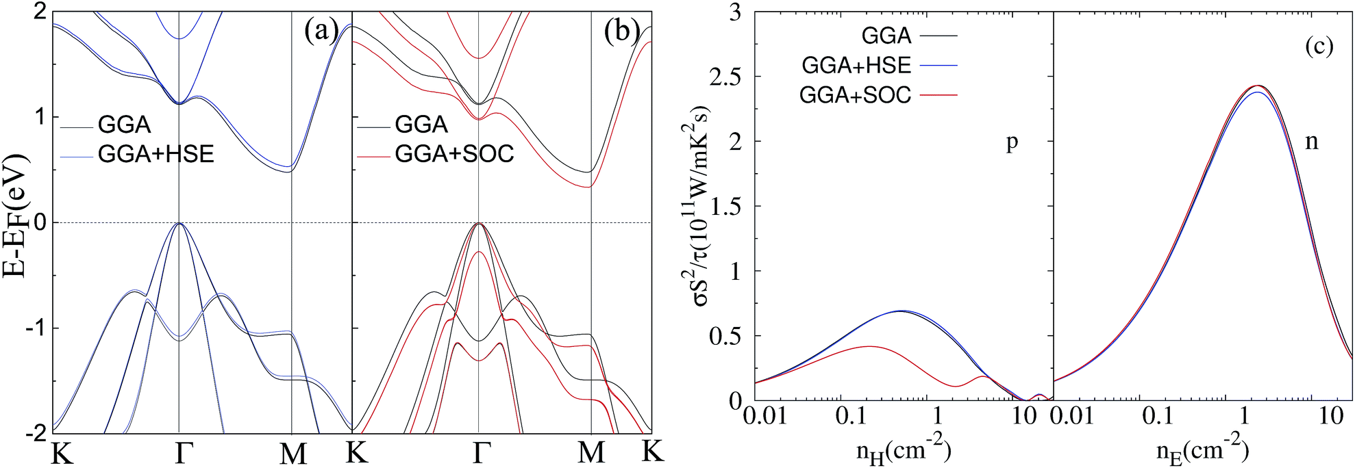 | ||
| Fig. 7 Calculated band structures of the ZrSe2 monolayer using the HSE hybrid functional (a) and SOC effect (b), also with a comparison to the normal GGA functional. (c) A comparison of power factor at room temperature predicted from different methods of GGA, HSE and SOC. | ||
With regard to the SOC effect, the difference of band structure lies in the uppermost two valence bands at the Γ point. They are degenerate at Γ without SOC, while they split into two individual bands when considering the SOC effect. This influence of SOC is similar to the situation in the bulk systems.58 Regarding the power factor, we find that there is little difference for n-type, while the p-type power factor decreases when considering the SOC effect. The decrease of the p-type power factor is due to the decreased band degenerate level of the two uppermost valence bands at the Γ point. Overall, the HSE functional has little influence on the thermoelectric transport performance, while the SOC effect may influence the p-type thermoelectric performance but it should not influence the strain dependence of the thermoelectric properties, which is the focus of this work.
Conclusions
In summary, based on first-principles calculations combined with Boltzmann equations, we have investigated the electrical, thermal and thermoelectric properties of monolayer ZrSe2 with and without biaxial tensile strain. The results reveal that at a strain of 7.5% the three valence band valleys converge in energy and the degeneracy of the valleys reaches a maximum, resulting in the maximum power factor (S2σ). Thus we obtain a maximum ZT of 4.58 and 3.84 for p- and n-type doping at room temperature, respectively, which are larger than those of the case without strain. Furthermore, these results verify our expectation that at the optimal strain, the values of ZT for monolayer ZrSe2 are larger than those of ZrS2 (2.4 for p-type and 1.8 for n-type doping)21 and HfS2 (3.67 for p-type and 3.08 for n-type doping).22 Above all, our studies indicate that the thermoelectric performance of a ZrSe2 monolayer can be effectively enhanced by band valley engineering through the application of biaxial strain. We can further conclude that at the optimal strain, the monolayer ZrSe2 is preferable to ZrS2 and HfS2 for thermoelectric transport due to the lower lattice thermal conductivity.Conflicts of interest
There are no conflicts to declare.Acknowledgements
The authors gratefully acknowledge the financial support from the National Natural Science Foundation of China (Grant No. 6137105 and Grant No. 51401031).References
- L. E. Bell, Science, 2008, 321, 1457–1461 CrossRef CAS PubMed.
- J. Sootsman, D. Chung and M. Kanatzidis, Angew. Chem., Int. Ed., 2009, 48, 8616–8639 CrossRef CAS PubMed.
- L. D. Hicks and M. S. Dresselhaus, Phys. Rev. B: Condens. Matter Mater. Phys., 1993, 47, 12727–12731 CrossRef CAS.
- L. Hicks and M. Dresselhaus, Phys. Rev. B: Condens. Matter Mater. Phys., 1993, 47, 16631 CrossRef CAS.
- G. Mahan and J. Sofo, Proc. Natl. Acad. Sci. U. S. A., 1996, 93, 7436–7439 CrossRef CAS.
- M. S. Dresselhaus, G. Chen, M. Y. Tang, R. Yang, H. Lee, D. Wang, Z. Ren, J.-P. Fleurial and P. Gogna, Adv. Mater., 2007, 19, 1043–1053 CrossRef CAS.
- G. J. Snyder and E. S. Toberer, Nat. Mater., 2008, 7, 105–114 CrossRef CAS PubMed.
- A. I. Hochbaum, R. Chen, R. D. Delgado, W. Liang, E. C. Garnett, M. Najarian, A. Majumdar and P. Yang, Nature, 2008, 451, 163–167 CrossRef CAS PubMed.
- Y. Dubi and M. Di Ventra, Rev. Mod. Phys., 2011, 83, 131 CrossRef CAS.
- X.-Y. Mi, X. Yu, K.-L. Yao, X. Huang, N. Yang and J.-T. LuÌĹ, Nano Lett., 2015, 15, 5229–5234 CrossRef CAS PubMed.
- Y. M. Brovman, J. P. Small, Y. Hu, Y. Fang, C. M. Lieber and P. Kim, J. Appl. Phys., 2016, 119, 234304 CrossRef.
- Y. Anno, Y. Imakita, K. Takei, S. Akita and T. Arie, 2D Mater., 2017, 4, 025019 CrossRef.
- A. Tabarraei, Comput. Mater. Sci., 2015, 108, 66–71 CrossRef CAS.
- R. Fei, A. Faghaninia, R. Soklaski, J.-A. Yan, C. Lo and L. Yang, Nano Lett., 2014, 14, 6393–6399 CrossRef CAS PubMed.
- W. Huang, H. Da and G. Liang, J. Appl. Phys., 2013, 113, 104304 CrossRef.
- J. Maassen and M. S. Lundstrom, Nanotechnology (IEEE-NANO), 2014 IEEE 14th International Conference on, 2014, pp. 904–907 Search PubMed.
- K. Ghosh and U. Singisetti, J. Appl. Phys., 2015, 118, 135711 CrossRef.
- Z. Jin, Q. Liao, H. Fang, Z. Liu, W. Liu, Z. Ding, T. Luo and N. Yang, Sci. Rep., 2016, 5, 18342 CrossRef PubMed.
- S. Kumar and U. SchwingenschlÃűgl, Chem. Mater., 2015, 27, 1278–1284 CrossRef CAS.
- G. Ding, G. Y. Gao, Z. Huang, W. Zhang and K. Yao, Nanotechnology, 2016, 27, 375703 CrossRef PubMed.
- H. Y. Lv, W. J. Lu, D. F. Shao, H. Y. Lu and Y. P. Sun, J. Mater. Chem. C, 2016, 4, 4538–4545 RSC.
- H. Lv, W. Lu, X. Luo, H. Lu, X. Zhu and Y. Sun, arXiv preprint arXiv:1608.05464, 2016.
- H. Goldsmid, Thermoelectric refrigeration, The International cryogenics monograph series, 1964 Search PubMed.
- D. M. Rowe, CRC handbook of thermoelectrics, CRC press, 1995 Search PubMed.
- F. J. DiSalvo, Science, 1999, 285, 703–706 CrossRef CAS PubMed.
- Y. Pei, X. Shi, A. LaLonde, H. Wang, L. Chen and G. J. Snyder, Nature, 2011, 473, 66–69 CrossRef CAS PubMed.
- Y. Pei, H. Wang and G. Snyder, Adv. Mater., 2012, 24, 6125–6135 CrossRef CAS PubMed.
- S.-D. Guo, J. Mater. Chem. C, 2016, 4, 9366–9374 RSC.
- G. Zhang and Y.-W. Zhang, Mech. Mater., 2015, 91, 382–398 CrossRef.
- R. Roldán, A. Castellanos-Gomez, E. Cappelluti and F. Guinea, J. Phys.: Condens. Matter, 2015, 27, 313201 CrossRef PubMed.
- H. Balout, P. Boulet and M.-C. Record, J. Electron. Mater., 2013, 42, 3458–3466 CrossRef CAS.
- H. Guo, N. Lu, L. Wang, X. Wu and X. C. Zeng, J. Phys. Chem. C, 2014, 118, 7242–7249 CAS.
- G. Kresse and J. Furthmüller, Phys. Rev. B: Condens. Matter Mater. Phys., 1996, 54, 11169 CrossRef CAS.
- J. P. Perdew, K. Burke and M. Ernzerhof, Phys. Rev. Lett., 1996, 77, 3865–3868 CrossRef CAS PubMed.
- Y.-S. Kim, M. Marsman, G. Kresse, F. Tran and P. Blaha, Phys. Rev. B: Condens. Matter Mater. Phys., 2010, 82, 205212 CrossRef.
- P. Blaha, K. Schwarz, G. Madsen, D. Kvasnicka and J. Luitz, WIEN2k An augmented plane wave+ local orbitals program for calculating crystal properties, 2001 Search PubMed.
- J. Heyd, G. E. Scuseria and M. Ernzerhof, J. Chem. Phys., 2003, 118, 8207–8215 CrossRef CAS.
- G. K. Madsen and D. J. Singh, Comput. Phys. Commun., 2006, 175, 67–71 CrossRef CAS.
- L. Xi, Y. B. Zhang, X. Y. Shi, J. Yang, X. Shi, L. D. Chen, W. Zhang, J. Yang and D. J. Singh, Phys. Rev. B: Condens. Matter Mater. Phys., 2012, 86, 155201 CrossRef.
- D. Parker and D. J. Singh, Phys. Rev. X, 2011, 1, 021005 Search PubMed.
- H. Peng, N. Kioussis and G. J. Snyder, Phys. Rev. B: Condens. Matter Mater. Phys., 2014, 89, 195206 CrossRef.
- H.-S. Kim, Z. M. Gibbs, Y. Tang, H. Wang and G. J. Snyder, APL Mater., 2015, 3, 041506 CrossRef.
- A. Togo, F. Oba and I. Tanaka, Phys. Rev. B: Condens. Matter Mater. Phys., 2008, 78, 134106 CrossRef.
- W. Li, N. Mingo, L. Lindsay, D. A. Broido, D. A. Stewart and N. A. Katcho, Phys. Rev. B: Condens. Matter Mater. Phys., 2012, 85, 195436 CrossRef.
- W. Li, L. Lindsay, D. Broido, D. A. Stewart and N. Mingo, Phys. Rev. B: Condens. Matter Mater. Phys., 2012, 86, 174307 CrossRef.
- W. Li, J. Carrete, N. A. Katcho and N. Mingo, Comput. Phys. Commun., 2014, 185, 1747–1758 CrossRef CAS.
- H. Guo, N. Lu, L. Wang, X. Wu and X. C. Zeng, J. Phys. Chem. C, 2014, 118, 7242–7249 CAS.
- K. Ghosh and U. Singisetti, J. Appl. Phys., 2015, 118, 135711 CrossRef.
- F. Beleznay, F. Bogár and J. Ladik, J. Chem. Phys., 2003, 119, 5690–5695 CrossRef CAS.
- L.-C. Zhang, G. Qin, W.-Z. Fang, H.-J. Cui, Q.-R. Zheng, Q.-B. Yan and G. Su, Sci. Rep., 2016, 6, 19830 CrossRef CAS PubMed.
- S.-D. Guo and J.-L. Wang, RSC Adv., 2016, 6, 31272–31276 RSC.
- A. Ward, D. A. Broido, D. A. Stewart and G. Deinzer, Phys. Rev. B: Condens. Matter Mater. Phys., 2009, 80, 125203 CrossRef.
- X. J. Tan, G. Q. Liu, H. Z. Shao, J. T. Xu, B. Yu, H. C. Jiang and J. Jiang, Appl. Phys. Lett., 2017, 110, 143903 CrossRef.
- Y. Y. Hui, X. Liu, W. Jie, N. Y. Chan, J. Hao, Y.-T. Hsu, L.-J. Li, W. Guo and S. P. Lau, ACS Nano, 2013, 7, 7126–7131 CrossRef CAS PubMed.
- G. Plechinger, A. Castellanos-Gomez, M. Buscema, H. S. van der Zant, G. A. Steele, A. Kuc, T. Heine, C. Schüller and T. Korn, 2D Mater., 2015, 2, 015006 CrossRef.
- R. Frisenda, M. Drüppel, R. Schmidt, S. M. de Vasconcellos, D. P. de Lara, R. Bratschitsch, M. Rohlfing and A. Castellanos-Gomez, arXiv preprint arXiv:1703.02831, 2017.
- Y. Pei, A. D. LaLonde, N. A. Heinz, X. Shi, S. Iwanaga, H. Wang, L. Chen and G. J. Snyder, Adv. Mater., 2011, 23, 5674–5678 CrossRef CAS PubMed.
- G. Yumnam, T. Pandey and A. K. Singh, J. Chem. Phys., 2015, 143, 234704 CrossRef PubMed.
| This journal is © The Royal Society of Chemistry 2017 |