
 Open Access Article
 This Open Access Article is licensed under a Creative Commons Attribution-Non Commercial 3.0 Unported Licence
Recent progress in the preparation and application of quantum dots/graphene composite materials
Ling Tong abc,
Feng Qiu*abce,
Tianjian Zengabc,
Jia Longabc,
Jie Yangabc,
Rongfei Wangabc,
Jin Zhangbcd,
Chong Wang*abc,
Tao Sun*abcd and
Yu Yang*abcd
abc,
Feng Qiu*abce,
Tianjian Zengabc,
Jia Longabc,
Jie Yangabc,
Rongfei Wangabc,
Jin Zhangbcd,
Chong Wang*abc,
Tao Sun*abcd and
Yu Yang*abcd
aInstitute of Optoelectronic Information Materials, School of Materials Science and Engineering, Yunnan University, Kunming 650091, China. E-mail: fengqiu@ynu.edu.cn; t.sun@griffith.edu.au
bInternational Joint Research Center for Optoelectronic and Energy Materials, Yunnan University, Kunming 650091, China
cYunnan Key Laboratory for Micro/Nano Materials & Technology, Yunnan University, Kunming 650091, China. E-mail: cwang@ynu.edu.cn
dSchool of Energy, Yunnan University, Kunming 650091, China. E-mail: yuyang@ynu.edu.cn
eNational Laboratory for Infrared Physics, Shanghai Institute of Technical Physics, Chinese Academy of Sciences, Shanghai 200083, China
First published on 12th October 2017
Abstract
Quantum dots/graphene (QDs/GR) composite materials show a distinct synergistic effect between the QDs and graphene, which has aroused vast attention toward their unique characteristics in the last few decades. The separation of electron–hole pairs generated in QDs are enhanced due to the photogating effects in the composites, and then the electrons or holes are rapidly transferred to the surface of the graphene sheets, resulting in excellent optical gain, making them promising materials for applications in optoelectronic and light harvesting devices. In this review, recent research progress on QDs/GR composites is reviewed and discussed, including preparation methods and applications. Numerous self-assembly synthetic methods such as hydrothermal, solvothermal, atomic layer deposition, ion beam sputtering deposition, and other typical synthetic methods like drop-casting, spin-coating, layer by layer, ultrasonication, polymethylmethacrylate (PMMA) aid transfer and electrochemical methods are summarized and discussed. In addition, the applications of QDs/GR composites such as in photodetectors, lithium ion batteries, solar cells, photocatalysis, electrochemiluminescence (ECL) sensors and supercapacitors are described in detail. Finally, the prospects of QDs/GR composites are discussed.
1 Introduction
Quantum dots (QDs) are zero dimensional materials with three dimensional confined carriers. The sizes of QDs are in the order of the exciton Bohr radius. Because of their novel structures, QDs possess various unique physical properties, including surface effects, quantum confinement effects, Coulomb blockade effects, quantum Hall effects, quantum tunneling effects and so on.1 These extraordinary properties have impelled the wide use of QD materials in optoelectronic devices such as photoelectric detectors,2 lasers,3,4 solar cells5–7 and illumination displays.8,9 Furthermore, these applications have also promoted research on the physical chemistry properties and applications of QD materials in recent years.10–13Graphene (GR) is known as a brilliant carbon material, patterned in a 2D honeycomb lattice.14 Novoselov and Geim et al. have successfully prepared freestanding graphene by the micromechanical cleavage method;15 the research on graphene and its various derivatives has become a hot topic globally. Due to its unique properties such as high carrier mobility (∼1 × 103 cm2 V−1 s−1), high specific surface area and excellent optical transparency, graphene is prospected as an ideal photonic and optoelectronic material,16 and is successfully applied in optoelectronic devices17 and energy storage devices.18 Because of its various advantages, more and more devices will be equipped with graphene or graphene-based composite materials in the future. Nevertheless, QDs and graphene also have their disadvantages. The low carrier mobilities limit the optical gain of QDs materials. Graphene also has drawbacks that cannot be ignored, like its low light absorption, the ultrafast recombination of photo-generated carriers, ease of aggregation and low dispersion. These shortages hinder the use of these two materials in future optoelectronic devices. In recent years, graphene-based nanocomposites combined with nanoparticles have attracted significant attention. Since QDs/GR composite materials were synthesized in 2010,19,20 these drawbacks of QDs and graphene have been completely overcome by the synergistic effects of the composite materials. In this hybrid structure, the QDs act as light-absorbing materials to produce electron–hole pairs under the irradiation of light. The carriers can then be rapidly transferred to graphene and produce photocurrent, leading to the efficient separation of electrons and holes and the prolongation of the lifetime of the carriers. The photo-generated carriers in QDs can therefore be effectively transferred to the surface of graphene sheets, which results in high optical gain, excellent optical response and good photo catalytical activities (shown in Scheme 1(a)–(c)). The charge transfer mechanism is the basic principle in the QDs/GR hybrid system. Based on the synergetic and cooperative effects of the hybrid, some new phenomena and physical properties can be inspired. Owing to their excellent performances, graphene inorganic nanocomposites have become a new class of electrocatalysts.21 QDs/GR composite materials can therefore provide a novel strategy for low-cost and high performances for potential applications in optoelectronic and light harvesting devices.19,22,23 Recently, these materials have been applied in photodetectors,24–27 lithium ion batteries,28,29 solar cells,30,31 photocatalysis,32,33 ECL sensors34 and other devices.
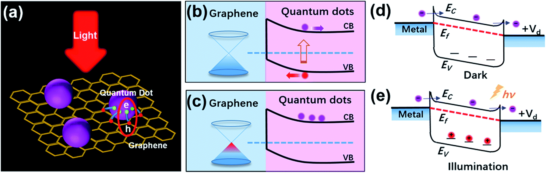 | ||
| Scheme 1 (a) Schematic illustration of the QDs/GR composite and light-generated electron–hole pairs. Energy level diagrams of the QDs/GR interface showing (b) electron–hole pair generation in QDs under illumination and (c) graphene doping induced by trapped carriers. Schematic of the photogating effect (d) under external bias in the dark and (e) under illumination. | ||
Aktürk et al. using first-principles calculations, demonstrated that Si and Ge atoms were bound at the bridge sites on graphene with binding energies of 0.54 eV and 0.49 eV at a coverage of θ = 1/32.35 The variable energy of Si and Ge atoms was most likely diffused along the T B H T sites, and the energy barrier was too low to prevent the clustering of adatoms; however, the binding energy in the H site was higher than the energies of the T and B sites. The H site adatom proved to be the tightest to combine with C atoms in graphene, and Si atoms showed higher binding energies than Ge atoms, regardless of being in the H site or T site, as shown in Fig. 1(a). The energy bands and density of states in the coverage of θ = 1/32 are shown in Fig. 1(b). The doping of Si and Ge atoms changed the graphene band structure and narrowed the band-gap, which benefited the carrier migration. Besides, the unbalanced spins demonstrated the charge transfer from adatoms to graphene.
 | ||
| Fig. 1 (a) Binding energy of Si and Ge adatoms in different sites, and their migration path. The adsorption sites were divided and named, top (T), bridge (B) and hollow (H), as shown in the map inserted in (a). (b) Energy band structure and total density of states of Si and Ge atoms adsorbed to graphene in the (4 × 4) supercell. Reprinted with permission from ref. 35. Copyright 2010 American Institute of Physics. | ||
The photogating effect was firstly discovered and named by Hou et al. using the analysis of microelectronic and photonic structures (AMPS) computer model in 1992.36 Their computer simulation results showed that this effect could be ascribed to the trapped charge and low field region in front of amorphous Si-based p–i–n structures under bias light illumination. They also demonstrated that the photogating effect was responsible for quantum efficiencies greater than unity. The photogating effect was further analyzed in forward biased a-Si:H Schottky barrier structures,37 reverse biased a-Si:H based p–i–n junctions38 and microcrystalline silicon (μc-Si:H) based n–i–p devices.39 It was found that the photogating effect was derived from band tail states in the conduction and valence bands of semiconductors, which were caused by structural defects and disordered interfaces. The band tails could also trap the photogenerated electrons/holes, prolong the lifetimes of carriers and form built-in fields, as shown in Scheme 1(d) and (e).40 In QDs/GR composites, photoconductive gain and responsivity could be effectively enhanced by the photogating effect, having huge potential for the application in optoelectronic devices.
In 2015, Khan et al. reviewed the synthesis, properties and applications of graphene based metal and metal oxide nanocomposites in detail.41 The preparation methods were broadly classified as top-down and bottom-up methods. The graphene-based inorganic nanocomposites show great potential in the wide-range applications of the electronics, electrochemical and electrical fields. In 2016, Shi et al. reported the synthesis and applications of 3D graphene-based composites.42 They mainly discussed the synthesis methods and applications in energy storage and conversion as electrode materials. At the same time, Pham et al. reviewed the graphene-semiconductor quantum dot hybrids in the application of photovoltaics and photodetectors.43 Particularly, the in situ and ex situ synthesis methods and charge transfer in hybrid systems were presented.
In this review, recent progress of QDs/GR composite materials, especially the synthesis method and its applications, are briefly reviewed. The challenges of the technique and its future development are discussed. Due to the unique synergistic effects between QDs and graphene, the QDs/GR composite materials have demonstrated excellent properties in optoelectronic, electrochemical and energy storage devices in recent years, and will be among the most promising hybrid materials in the near future.
2 Preparation methods
The conventional methods for synthesizing QDs are mainly chemical vapor deposition (CVD), sol–gel, molecular beam epitaxy (MBE), liquid phase epitaxy (LPE), etc. Graphene was initially produced by micromechanical exfoliation, but liquid-phase exfoliation, carbon segregation and CVD have been exploited in the last few decades; the QDs/GR composite materials can also be easily prepared by these methods. Self-assembly methods can transform these systems from the disordered to ordered state by their internal interactions, which are considered to be much more useful routes, and are described in detail in the following sections.Due to the high surface area and ultrahigh conductivity, graphene is often employed as a fine conductive layer in hybrid materials, in which electrons or holes can be effectively transferred, and leads to good photoelectric performances. However, pure graphene film has limited functional groups, and restrains the possibility for chemical modification. Thus, graphene oxide (GO) and reduced graphene oxide (rGO) have come to be ideal materials because they possess lots of oxygen-containing functional groups and defects, such as hydroxyl, carboxyl, carbonyl and epoxy groups, and numerous nano-scale materials can be associated with them via covalent or noncovalent bonds. GO and rGO are convenient for use in solvent processes to promote the syntheses of hybrid structure and aid the transfer of electrons or holes. The colloidal quantum dots (cQDs) can also possess lots of chemical bonds and ligands on its surface, which act as outstanding connecting mediums and carrier channels.
So far, numerous synthetic methods have been employed to prepare different QDs/GR composite materials; chemical methods are mainly used due to their low cost. These methods are summarized in Table 1.
| Synthetic methods | Materials | Applications | Ref. |
|---|---|---|---|
| Hydrothermal (SA) | CdTe QDs–TiO2–GR | Optoelectronics | 46 |
| Fe3O4@C QDs/GR | Lithium ion batteries | 29 | |
| SnO2 QDs@GO | Lithium ion batteries | 47 | |
| SnO2 QDs/GR | Lithium ion batteries | 50 | |
| CoS2 QDs/GR | Lithium ion batteries | 52 | |
| SnO2 QDs/GR | Photocatalysis | 48 | |
| N, S co-doped GQDs–rGO–TiO2 | Photocatalysis | 103 | |
| B- and N-doped GQDs/GO | Electrocatalysts | 51 | |
| GR–CdS QDs | Non-enzyme biosensor | 49 | |
| N-doped GQDs/GR | Electrocatalytic | 125 | |
| Solvothermal (SA) | rGO/CuInS2 QDs | Solar cells | 54 |
| MoS2 QDs–GR–TiO2 | Photocatalysis | 53 | |
| ZnO@GO | Photocatalysis | 55 | |
| Atomic layer deposition (SA) | ZnO QDs/GR | UV photodetectors | 56 |
| ZnO QDs/GR | Lithium ion batteries | 28 | |
| TiO2 QDs/GR | Photocatalysis | 104 | |
| IBSD (SA) | Ge QDs/GR | Optoelectronics | 57 |
| Drop-casting | CdSe/ZnS QDs/GR | Optoelectronics | 23 |
| ZnO cQDs/GR | UV photodetectors | 58 | |
| PbS cQDs/GR | Phototransistors | 22 and 59 | |
| Spin-coating | ZnO cQDs/GR | UV photodetectors | 61 |
| Ge QDs–GR–ZnO | Infrared photodetectors | 62 | |
| PbS cQDs/GR | Phototransistors | 63 | |
| Layer-by-layer | PbSe QDs/GR | Phototransistors | 64–66 |
| PbS QDs/GR | Phototransistors | 67 | |
| CdS QDs/GR | Photocatalysis | 32 | |
| Ultrasonic | CoO QDs/GR | Lithium ion batteries | 69 |
| SnO2 QDs/GR | Electrochemistry | 68 | |
| PMMA aided-transfer | GR/GeSi QDs | Optoelectronics | 70 and 71 |
| InAs/GaAs QDs/GR | Optoelectronics | 72 and 73 | |
| Electrochemical | GQDs–3D GR | Supercapacitors | 82 |
| NiO QDs/GR | Supercapacitors | 83 | |
| 3D GR/MnO2 | Supercapacitors | 119 | |
| ipGR/GQDs | Supercapacitors | 120 | |
| Microwave irradiation | Co3O4 QDs/GR | Lithium ion batteries | 86 |
| Printing | ZnO QDs/GR | UV photodetectors | 94 |
2.1 Self-assembly methods (SA)
Self-assembly methods have been widely employed for QDs synthesis, although the self-assembly concept was first used in bioscience. Self-assembly involves processes that can promote the disordered components turning into ordered patterns by their internal interactions. It has three remarkable features: (I) the components may react directly toward a high ordered state; (II) the weak interactions such as, van der Waals π–π, hydrogen bonds, etc., play important roles in determining their physical properties; (III) the building blocks are broad, and not only include atoms and molecules, but also contain nano- and mesoscopic structures.To date, numerous trials have been carried out to develop new materials for adopting self-assembly methods. The synthetic routes are designed to expand applications and cut costs; some typical self-assembly methods such as hydrothermal, solvothermal, atomic layer deposition, ion beam sputtering deposition, are introduced and summarized.
Zhao et al.47 recently employed GO as a template for growing oxidized SnO2 QDs. Sn2+ ions were oxidized by the functional groups of GO, and GO was applied as the template for promoting selective heterogeneous nucleation; the produced SnO2 nanoparticles were nucleated and grown on the surface of GO. The SnO2 QDs@GO composite was formed during the hydrothermal process, as illustrated in Fig. 2(a). Fig. 2(b) shows the transmission electron microscopy (TEM) image of SnO2 QDs@GO with good dispersion and high mass loading. As shown in Fig. 2(c) and (d), SnO2 QDs preferred to grow along the [001] direction, with (110) surfaces as oxygen bridging sites on the SnO2 (110) plane. After assembling into LIBs, the huge volume expansion/contraction of lithium-ion batteries during the processes of discharging/charging was effectively released. This composite was also beneficial for fast lithium intercalation/de-intercalation, due to the existence of graphene.
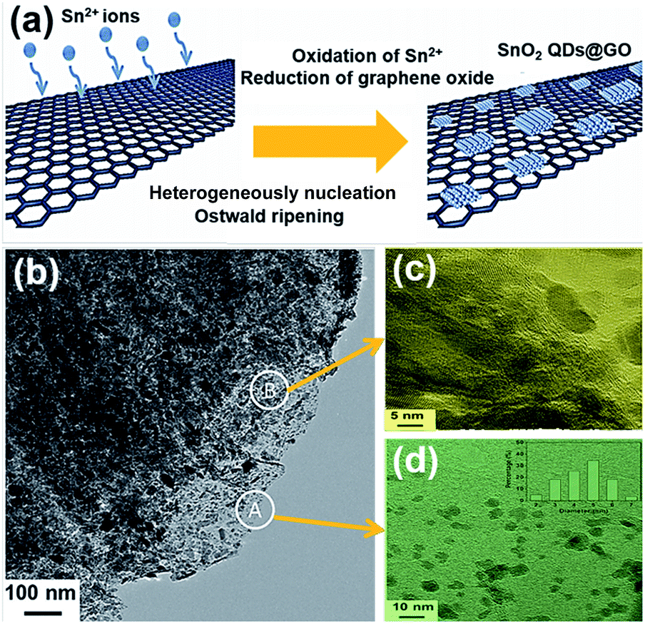 | ||
| Fig. 2 (a) Schematic illustration for the fabrication of SnO2 QDs@GO. (b) TEM image of SnO2 QDs@GO. (c), (d) High-resolution transmission electron microscope (HRTEM) of section B and A in image (b), respectively. The inset in image (d) is a size distribution image. Reprinted with permission from ref. 47. Copyright 2015 Wiley-VCH. | ||
In 2014, Zhang et al. reported that the GR–CdS QD hybrids could be used for non-enzyme biosensors via the one-step hydrothermal method.49 GO was first prepared from graphite by a modified Hummer's method, then mixed with 70 mL water to obtain the GO dispersions by the ultrasonication process. When the weight ratio of GO and Cd(CH3COO)2·2H2O was 0.5% (G0.5–CdS), the graphene–CdS QDs composite with a good distribution and high coverage rate was prepared via non-covalent bonding. In this process, thiourea and Cd(CH3COO)2·2H2O were employed as the sulphur source and cadmium source, respectively.
Polyacrylic acid (PAA), for example, possesses lots of carboxylic acid groups, which urges the link between QDs and GO and promotes the coverage rate and uniformity. It also benefits from the negative charges, such as COO− and OH−, because they can attach to CdS QDs to make them more stable.
As shown in Fig. 3(a), CdS QDs were excited, and yielded photo-generated electrons and holes under illumination, then the electrons were rapidly transferred to graphene film from the conduction band (CB) of CdS QDs. Graphene acted as the electron capture and transport matrix to avoid electron–hole recombination, resulting in prolonging the electron lifetime and high light sensitivity. In this process, the OH− was oxidized to OH by photo-generated holes, so that glucose was oxidized to gluconolactone by OH˙ and was further detected through different photocurrent densities (Fig. 3(d)). The lattice fringes of cubic CdS particles in the G0.5–CdS hybrid can be seen clearly in Fig. 3(b), while CdS QDs stacked randomly together when prepared without GO. It is believed that the graphene could promote crystal growth and in turn prevent itself aggregation with the CdS QDs loading. The G0.5–CdS/ITO electrode has long lifetime and high photocurrent density with glucose, as shown in Fig. 3(c) and (d).
 | ||
| Fig. 3 (a) Schematic diagram for the photoelectrochemical process of oxidation of glucose and electron transfer at the G0.5–CdS/ITO electrode. (b) HRTEM image of G0.5–CdS. (c) Electron lifetime versus open-circuit potential for the electrode without and with glucose. (d) Photocurrent density of the electrode in NaOH in the presence of different concentrations of glucose (concentration increased from bottom to top). Inset: linear calibration curve. Reprinted with permission from ref. 49. Copyright 2014 Elsevier Ltd. | ||
Liu et al. prepared the CdTe QDs–TiO2–graphene hybrid via a general hydrothermal method.46 The CdTe QDs–TiO2–graphene hybrid was fabricated by the in situ growth of CdTe QDs on the rGO–TiO2 composite surface. The fluorescence quenching of the produced hybrid indicates that the electrons transfer from CdTe QDs to TiO2 and graphene. Additionally, Ye et al. fabricated the SnO2 QDs/GR composite with visible light catalytic activity via a one-step, low cost and environment-friendly hydrothermal process48 that also avoided the agglomeration of QDs. Zhao et al. prepared a carbon-coated Fe3O4 QDs/GR composite by using a hydrothermal and calcining route.29 In this process, the carbon shell can prevent the aggregation and buffer the volume expansion, which improves lithium-storage performance.
Some novel technologies combined with hydrothermal methods have been employed in recent years. Huang et al. successfully fabricated the SnO2 QDs/GR composite via the electron-beam irradiation (EBI) technique combined with the hydrothermal method in 2015.50 The EBI was mainly used for irradiating the graphene nanosheets to increase the interlayer spacing; it also promoted exfoliation and removed the partial oxygen-containing functional groups. The SEM figures show that the SnO2 QDs were loaded on both sides of the graphene sheets with uniform dispersion. The high reversibility and specific capacity as well as good cycle response of this composite material promote its use in the energy storage field. Besides, the B- and N-doped graphene quantum dots/GO (GQDs/GO) composite was prepared via a self-assembled hydrothermal treatment in a sealed Teflon-lined autoclave, following the co-doping of B- and N- by high-temperature annealing.51 This hybrid could be applied as an excellent oxygen reduction electrocatalyst. He et al. synthesized CoS2 nanoparticles wrapped by CoS2 QDs/GR via an L-cysteine-assisted hydrothermal reaction.52 The CoS2 QDs/GR composite provided more active sites for the intercalation of lithium ions. The graphene in the composite demonstrated high transport abilities of electrons and lithium ions, and could also effectively suppress the volume expansion of CoS2 nanoparticles. Under their synergistic effect, this material exhibits excellent performances for the application of lithium-ion batteries.
In 2015, Gao et al. synthesized the MoS2 QDs–GR–TiO2 composite via the one-pot solvothermal method.53 Thiocarbamide was applied as the precursor, then mixed with Na2MoO4·2H2O and P25 powder. The formation mechanism of MoS2 QDs was ascribed to the interactions between the functional groups of GO and Mo precursors as shown in Fig. 4(a). The sizes of MoS2 QDs are 2 to 3 nm and the lattice fringes from the (100) planes of crystal MoS2 QDs can be observed. The MoS2 QDs–GR hybrid was introduced as a co-catalyst to overcome the low charge separation rate and large band gap caused by TiO2. It also enhanced the visible-light absorption, charge separation and photocatalysis ability, and significantly improved its photocatalysis properties.
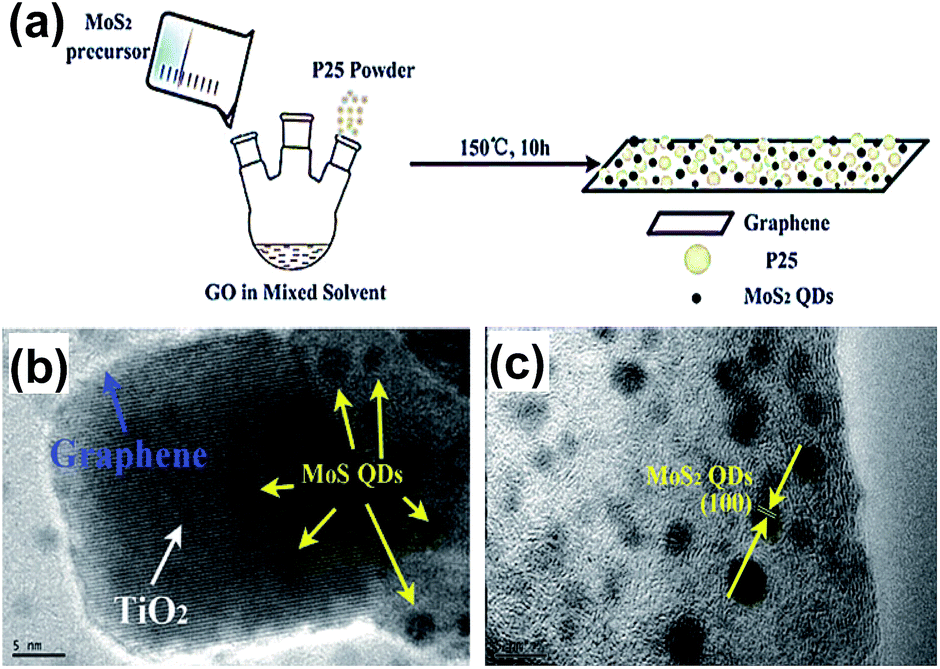 | ||
| Fig. 4 (a) Schematic demonstration of the fabrication of the MoS2 QDs–graphene–TiO2 composite. (b) HRTEM image of the MoS2 QDs–graphene–TiO2 composite. (c) HRTEM image of the MoS2 QDs–graphene hybrid. Reprinted with permission from ref. 53. Copyright 2015 Royal Society of Chemistry. | ||
Meng et al. synthesized the rGO/CuInS2 QD hybrid using thiourea as the S doping source and CS(NH2)2 as the precursor by the same approach.54 The GO films were reduced to rGO during the formation of CuInS2 QDs, and the adsorbed Cu+ was used for the nucleation of CuInS2 QDs. They deemed that the Cu2+ was mainly adsorbed at the epoxy/hydroxyl groups on GO at room temperature. The rGO/CuInS2 QD hybrid was a good electron acceptor in polymer-based solar cells. The efficiency of assembled solar cells was 1.5% higher, compared to the rGO sheet counterpart devices. Atchudan et al. fabricated the ZnO@GO composite via the solvothermal method.55 The GO sheet base was synthesized by utilizing the Hummers method, and the added ZnO nanoparticles were prepared by thermal oxidation. The ZnO nanoparticles were then impregnated into the GO surface for ZnO@GO composite preparation via the solvothermal process. The ZnO nanoparticle sizes were about 10–20 nm. This composite can be applied as a photocatalyst for organic dye degradation.
The one-pot solvothermal method is relatively simple and easy to control. The chemical reaction in this process could be carried out in a hermetic system, which could effectively prevent the volatilization of toxic substances and avoid air, for air sensitive precursors.
| ZnOH* + Zn(CH2CH3)2 → ZnOZn(CH2CH3)* + CH3CH3 | (1) |
| Zn(CH2CH3)* + H2O → ZnOH* + CH3CH3 | (2) |
Sun et al. prepared the ZnO QDs/GR composite by the same approach for enhancing the capacity of lithium storage.28 The growth rate of ZnO was about 2 Å per cycle, thus, it was easy to control the ZnO particle sizes during the ALD cycles. The fabricated ZnO QD sizes were 2 to 7 nm through the ALD process. The ALD reaction process and images for characterization are shown in Fig. 5. The sizes of ZnO nanoparticles were about 2 nm and 7 nm after 15 and 50 ALD cycles, respectively. The increase in the sizes was nearly a linear function of the cycling numbers. Previously, the ZnO nanoparticles were hard to nucleate directly on graphene, due to the unreactive properties of graphene. The ZnO nanoparticles were expected to nucleate at the edge planes and defects because of the probable lower energy on those sites.
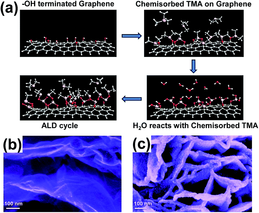 | ||
| Fig. 5 (a) Schematic diagram of ALD reaction. SEM images of the ZnO QDs/GR composite at 15 ALD cycles (b) and 50 ALD cycles (c). Reprinted with permission from ref. 28. Copyright 2014 Royal Society of Chemistry. | ||
 | ||
| Fig. 6 AFM images of the Ge QDs/GR composite at different sputtering times at room temperature: 60 s (a), 180 s (b) and 300 s (c). XPS image (d) and PL spectra (e) of the Ge QDs/GR composite grown at 500 °C. Reprinted with permission from ref. 57. Copyright 2016 IOP Publication Ltd. | ||
In general, the self-assembly methods that have been utilized to synthesize QDs/GR composites are efficient. It is critical to choose suitable building blocks and preparation processes. The chemical bonds that link QDs with graphene and provide the channels for the transfer of separated electrons or holes lead to the enhanced electrochemical and photoelectric properties, which satisfy the growing market requirements from industry, customers and the military.
Except for the SA methods, drop-casting, spin-coating, layer by layer, ultrasonic, PMMA aided-transfer and other typical methods may also be employed to synthesize QDs/GR composite materials. In recent years, tremendous efforts have been made for QDs/GR composite fabrication and property improvement via these methods. With the aid of external conditions, composites can be prepared via directional manipulation and fast reaction.
2.2 Drop-casting method
The drop-casting method is a frequently implemented strategy to prepare films. The procedure is as follows: several solutions are dropped onto a substrate without rotation, and are then heated for hours or annealed for several minutes to remove water. In recent years, some groups have successfully prepared QDs/GR composites such as the CdSe/ZnS QDs/GR composite,23 the colloidal ZnO QDs/GR composite,58 the PbS QDs/GR composite22,59 and giant nanocrystal QDs/GR composite,60 using this method.In 2015, Gromova et al. prepared colloidal core/shell CdSe/ZnS QDs by hot-injection synthesis, and multi-layer graphene flakes were prepared by ultrasound processing of graphite.23 The solution containing CdSe/ZnS QDs material was deposited on the multi-layer graphene sheets to fabricate the CdSe/ZnS QDs/GR composite via the drop-casting method. The extraordinary mechanical properties are as a result of the multi-layer graphene structure, which causes the composite to be easily processed in solution; the hybrid structure enhances the photoelectrical response.
Son et al. fabricated ultraviolet (UV) photodetectors using the ZnO cQDs/GR hybrid.58 Firstly, the GR/PET virtual substrate was fabricated using PMMA to transfer graphene onto the PET substrate, then the solution containing ZnO cQDs was deposited onto the surface of graphene to fabricate the ZnO cQDs/GR composite. The synthesis process is shown in Fig. 7(a). This composite possessed a high optical transmittance (∼80%) and good flexibility (Fig. 7(b)). The HRTEM image suggests that the colloidal ZnO QDs are tightly attached to the surface of the graphene sheet, as shown in Fig. 7(c).
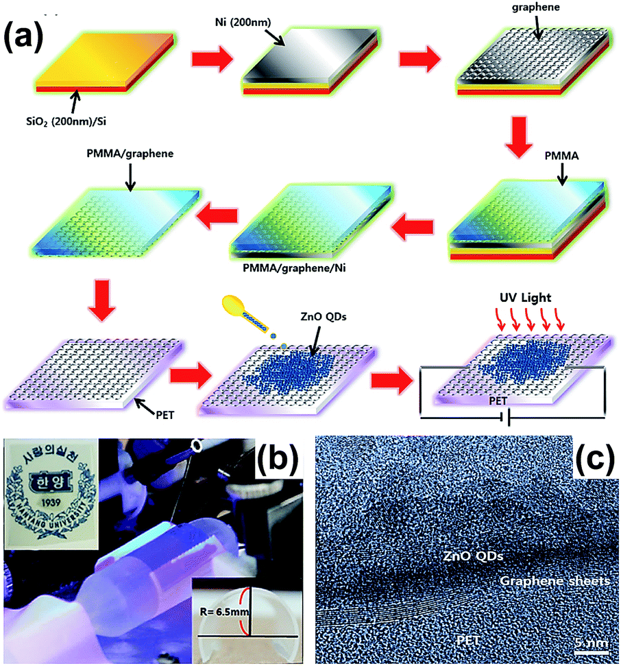 | ||
| Fig. 7 (a) Illustration of the preparation of the ZnO QDs/GR composite. (b) Images of the equipment and device; the inset on the bottom right shows a flexible UV photodetector. (c) HRTEM image of the ZnO cQDs/GR composite on a polyethylene terephthalate (PET) substrate. Reprinted with permission from ref. 58. Copyright 2015 Elsevier Ltd. | ||
Turyanska et al. employed ligands to combine colloidal PbS QDs with graphene for fabricating the PbS cQDs/GR hybrid using the drop-casting method.59 Various ligands such as polyethylene glycol, thioglycerol (TGL) and 2,3-dimercapto-1-propanol (DTG) with different lengths were explored. Polyethylene glycol H–(O–CH2–CH2)n–OH with n = 2000 and n = 500 was denoted QDP2000 and QDP500; the corresponding lengths were 10 and 5 nm, respectively. The QDTGL represents the thioglycerol capped QDs with 0.5 nm length. As shown in Fig. 8, the graphene Fermi energy increased by +50 meV, but was still below the QD LUMO state after depositing QDP2000 and QDP500; the conduction was p-type at Vg = 0 after current versus Vg characteristics and calculations. The photo-generated electrons in QDs were transferred to graphene's LUMO energy level (Fig. 8(b)). When QDTGL was deposited, the Fermi energy shifted by +300 meV, and the conduction became n-type at Vg = 0; the photo-generated holes in QDs preferred to be transferred to the graphene sheet (Fig. 8(c)). The characteristics in Fig. 8(d) indicate ultra-high responsivity (∼109 A W−1), which is two orders higher than in other previous reports. This extraordinary performance can be ascribed to the charge transfer from QDs and the accumulation of charge. The responsivity of the transistor can also be enhanced by choosing ligands of suitable length and preserving their integrity.
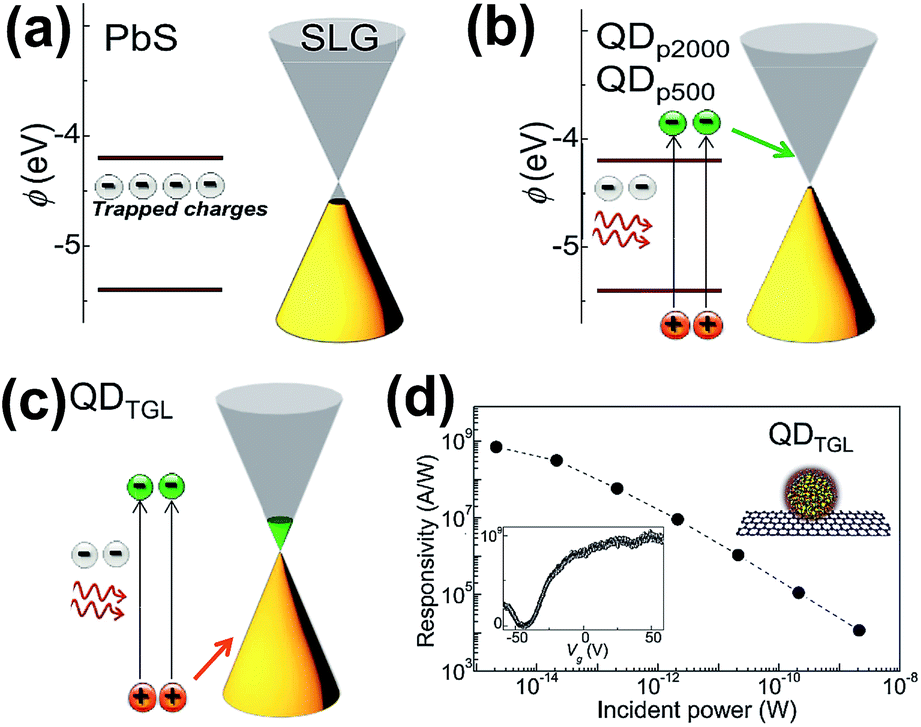 | ||
| Fig. 8 Schematic illustration of the energy states (a) before depositing QDs on graphene, (b) after depositing QDP2000 and QDP500 on graphene and (c) after depositing QDTGL on graphene. (d) Photoresponsivity as a function of the incident light power of the QDTGL/GR transistor device. The bottom left inset shows photoresponsivity as a function of gate voltage (Vg). Reprinted with an Open Access from ref. 59. Published by WILEY-VCH Verlag Gmbh & Co. KGaA, 2015. | ||
2.3 Spin-coating method
The spin-coating method is another similarly useful path to drop-casting. The difference between them is that this process requires a rotating substrate for spin-coating. The thickness of the film can be easily controlled by rotating speed and running time.Ultraviolet (UV) photodetectors based on a colloidal ZnO QDs/GR hybrid have been fabricated via the wet spin-coating process.61 The colloidal ZnO QDs were synthesized and dropped onto the graphene flakes, then the composite was annealed for few minutes for residual solvent elimination. The distribution of ZnO QDs was uniform on the graphene sheets. The final manufactured UV photodetector showed a high ratio of the photocurrent to the dark current (∼1.1 × 10⁴).
Liu et al. fabricated an infrared photodetector on a flexible substrate by the analogic method.62 The Ge QDs–GR–ZnO heterostructure resulted in high responsivity (∼9.7 A W−1) in a shortwave infrared field (1400 nm) and fast response speed (∼40 μs rise time and 90 μs recovery time). Konstantatos et al.63 fabricated phototransistors based on a PbS cQDs/GR hybrid; the specific detectivity was up to 7 × 10¹³ Jones, benefitting from the photogating effect of the trapped electrons in PbS QDs and forming a built-in field at the QDs/GR interface, the responsivity was 107 A W−1.
2.4 Layer by layer method
The layer by layer (LbL) method is an effective strategy for obtaining the multilayer QDs/GR hybrid structure, and many hybrids have been employed for field effect phototransistors (FEpTs) in recent years. For realizing ultrahigh photoresponsivity, the QDs acted as the light absorption layer, and graphene was the charge transfer layer. Zhang et al. designed a PbSe QDs/GR hybrid;64 a wet chemical method was applied for PbSe QDs preparation and the graphene was prepared by a CVD technique and subsequently transferred to the substrate. One drop of PbSe QD solution was deposited on a rotating substrate, and then three drops of ethanedithiol (EDT) solution were placed on the same substrate for ligand exchange. Four layers of PbSe QDs were deposited on graphene. The absorption and emission peaks were 1616 nm and 1645 nm, respectively. The electrons and holes of the produced FEpTs achieved high mobilities and the light responsivity was 1 A W−1.In 2015, two types of multi-heterojunction FEpTs were prepared based on a PbSe QDs/GR hybrid with different layer arrangements via the same approach, denoted QD-bottom and G-bottom.65 Fig. 9(a)–(d) shows the schematic diagrams and cross-sectional SEM images of QD-bottom FEpTs and G-bottom FEpTs. The thickness of the SiO2 layer was 300 nm, and the thickness of the QD-bottom FEpTs (109 nm) was close to G-bottom FEpTs (103 nm), which demonstrated that the uniformity of the QDs is better than for graphene in the first layer with thickness of 103 nm. There were slight point shifts for QD-bottom FEpTs and large negative shifts for G-bottom FEpTs, as shown in the transfer characteristic curves in Fig. 9(e). As is well known, the shift degree is related to the QD surface defects, the degree of energy level matching and the barriers induced by ligands. The changes in the transfer curve demonstrate that the carriers were transferred from QDs to graphene following the Dirac point shift. Fig. 9(f) shows that the responsivity was up to 106 A W−1; the G-bottom layer demonstrated multi-saturation behaviour, due to the back-gate effect.
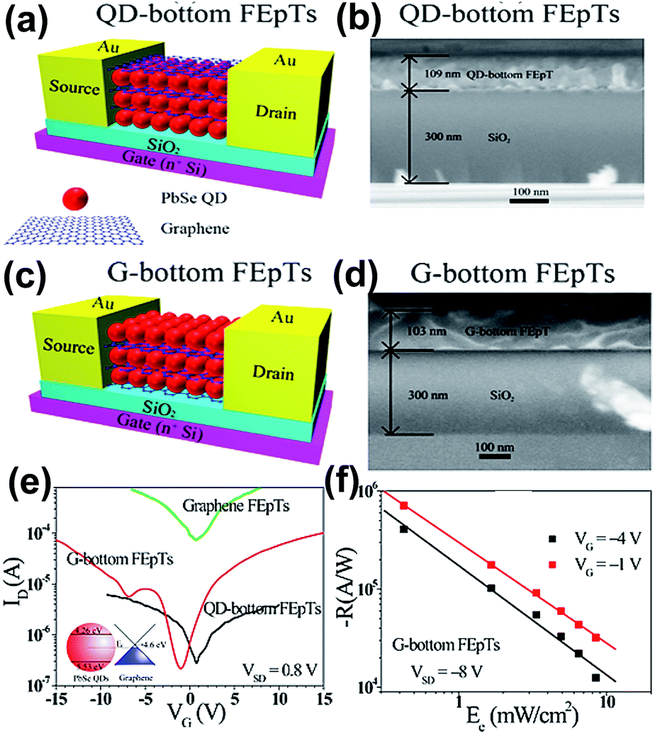 | ||
| Fig. 9 Schematic diagram of QD at the bottom layer FEpTs (a) and the corresponding cross-sectional SEM images of the multi-heterojunction channel (b). Schematic diagram of graphene at the bottom layer of FEpTs (c) and the corresponding cross-sectional SEM images of the multi-heterojunction channel (d). (e) Transfer characteristics of graphene FEpTs, G-bottom FEpTs and QD-bottom FEpTs without light illumination. (f) Responsivity as a function of illumination of the G-bottom FEpTs. Reprinted with permission from ref. 65. Copyright 2015 American Chemical Society. | ||
The same group also reported another two types of multi-heterojunction FEpTs based on the same hybrid material to compare their photoresponse properties.66 They demonstrated that the layered heterojunction FEpTs were better candidates for near infrared phototransistors than bulk heterojunction FEpTs. Meanwhile, the wide spectral response FEpTs based on PbS QDs/GR hybrids were also investigated by the above group via the layer by layer method.67 Because of the multiple-exciton generation of PbS QDs and its synergistic effects with graphene, the assembled FEpTs achieved a wide spectral response (300–1400 nm) and high responsivity (2 × 10⁵ A W−1 at 10 mV bias voltage).
The layer by layer strategy can also be employed for self-assembly. In 2004, Liu et al. successfully fabricated a CdS QDs/GR hybrid to study its photoelectrochemical and photocatalytic properties.32 In the fabrication processes, the graphene flakes were obtained by reduction of graphite oxide, then the clean substrate was dipped into CdS QDs mixed with thioglycolic acid (TGA) solution and graphene nanosheets-poly(allylamine hydrochloride) (PAH) solution. These procedures were repeated to fabricate the multi-layered films. The photocatalytic and photoelectrochemical activities of the new CdS QDs/GR multilayered were remarkably enhanced.
2.5 Ultrasonic method
The ultrasonic method is another effective technique for QDs/GR composite material preparation. Chen et al. fabricated a SnO2 QDs/GR composite via a facile one-step ultrasonic approach by using SnCl2·2H2O as the precursor.68 The sizes of the SnO2 QDs were 4–6 nm, and the synthesized QDs were uniformly dispersed on both sides of the graphene. The schematic of the mechanism of formation is shown in Fig. 10(a). Firstly, the Sn2+ ions of the SnCl2 solution combined with GO through electrostatic attraction to the carbonyl and carboxyl groups, then ultrasonic vibration was used to increase the interlayer space to make Sn2+ migrate into the enlarged layer, which resulted in prohibiting the GO stacks and enhancing the Sn2+ loading number. Finally, the SnO2 QDs/GR composite was obtained through a calcination treatment. Fig. 10(b) shows the uniformly distributed SnO2 QDs on the graphene sheet with good crystallinity. In Fig. 10(c), the lattice fringes can be clearly observed, indicating that the SnO2 was well-crystallized with the rutile phase (110) face. The typical XRD patterns are shown in Fig. 10(d); the bare graphene sheets (#1) showed a strong (002) diffraction peak, and the similarity of the diffraction peaks of the SnO2 QDs/GR hybrid (#2) and SnO2 nanoparticles (#3) indicates that the SnO2 QDs were well-crystallized in the hybrid. However, the (002) diffraction peak is not sharp in the XRD of the SnO2 QDs/GR hybrid (#2), which might be caused by the graphene sheets' regular lamellar structure, which was broken and turned into exfoliated graphene in the synthetic processes. These phenomena also indicate that both sides loaded with SnO2 QDs by this novel method can prevent graphene restacking during the reduction process and the graphene also prevents agglomeration of SnO2 QDs during the calcination. The ultrasonication mainly provides the driving force to enlarge the interlayer spacing of graphene, and supplies more effective loading sites for SnO2 QDs on the graphene surface. Additionally, the ultrasonication could also prevent graphene stacking.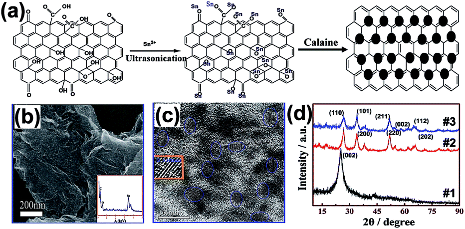 | ||
| Fig. 10 (a) Schematic diagram of the formation of a SnO2 QDs/GR hybrid. (b) Field emission-secondary electron microscopy (FE-SEM) image of the SnO2 QDs/GR hybrid on the Si (100) substrate. (c) HRTEM image of the SnO2 QDs/GR hybrid. (d) XRD patterns of bare graphene sheets (#1), SnO2 QDs/GR hybrid (#2) and SnO2 nanoparticles (#3). Reprinted with permission from ref. 68. Copyright 2013 American Chemical Society. | ||
Sonication can be used to provide energy for decomposition in the hybrid process. In 2012, Peng et al. employed Co4(CO)12 as the cobalt precursor and synthesized a CoO QDs/GR composite by the ultrasonic method.69 The mechanism of the material formation can be divided into two steps: (I) Co was produced by the decomposed Co4(CO)12 precursor, and deposited on the surface of the graphene sheet with the assistance of sonication. (II) Co was oxidized in situ into CoO. The successful fabrication is ascribed to the strong interaction between electron-rich Co atoms and graphene's electrophilic carbon atoms. The sizes of CoO QDs were 3 to 8 nm, and the QDs were well-dispersed on the graphene surface. The obtained composite inhibits the aggregation of graphene and the volume changes of MOx during the cycling test of lithium-ion batteries. As anode material, this composite demonstrates a highly reversible lithium storage capacity and outstanding cycling stability.
2.6 Polymethylmethacrylate (PMMA) aided-transfer method
Polymethylmethacrylate (PMMA) is a widely used medium for graphene transfer. The procedures can be divided into three steps as follows: (I) PMMA/GR/substrate is constructed into the sandwich-structure, (II) etching solution or organic solvent is removed from the substrate, (III) PMMA is dissolved in acetone solution or organic solvent.In 2015, Chen et al. successfully fabricated the GR/GeSi QDs composite by using a PMMA aided-transfer method.70 Ten-layered GeSi QDs were prepared on Si (001) substrates by the MBE technique, and the graphene sheet was grown by the CVD technique. The monolayer graphene sheet was transferred onto the GeSi QDs surface with the aid of PMMA. The manufactured device structure is shown in Fig. 11(a) and the uniform size distribution of GeSi QDs can be observed in the AFM image. The average size and height of the surface QDs was about 100 and 7 nm, respectively. The schematic energy band diagram of this composite is shown in Fig. 11(b). The potential distribution could promote the separation of photo-generated electron–hole pairs, and the added electric field could reduce the graphene Fermi level, thus the electrons can be transferred from QDs to graphene more easily. The decrease in PL Intensity from 0 to −40 V also demonstrated the enhancement of electron transfer, as shown in Fig. 11(c). It was found that the luminescence properties of the composite can be adjusted by laser energy and graphene plasmon with the external vertical field. Similarly, they fabricated the GR/GeSi QD hybrid structures via the same path in 2014.71 In particular, a 10-layer GeSi QDs sample was divided into two equal parts, one of them was covered by graphene, and the other part was uncovered. The surface-plasmon-polariton (SPP) enhanced absorption mechanism was proposed to illustrate the enhancement of the photoluminescence (PL) intensity of the graphene/GeSi QD hybrid.
 | ||
| Fig. 11 (a) Schematic illustration of the structure of the ten-layer GeSi QDs/GR composite device and the corresponding AFM image of the top layer GeSi QD sample. (b) Schematic diagrams of energy band alignment under negative voltage. (c) PL spectra of the hybrid structure under −40 to 40 V voltage at different temperatures. Reprinted with an Open Access from ref. 70. Copyright 2015 Springer Nature. | ||
This method was also used to prepare the InAs/GaAs QDs/GR composite.72,73 Ajlani et al. synthesized the graphene-capped InAs/GaAs QDs hybrid by this method. InAs QDs were grown by the MBE technique on a GaAs (001) substrate, and multilayer graphene flakes were grown by the CVD technique. The multilayer graphene flakes were transferred onto QDs with the aid of PMMA, and uncapped QDs were designed for comparison. The enhancement of PL was observed, which indicated electron transfer from graphene to QDs. On the other hand, the presence of the cap layer modified the appearance of the QDs, and prevented the surface oxidation; it also acted as the active layer in a laser device.
2.7 Electrochemical method
Electrochemical synthesis is an effective strategy for synthesizing nano-scale materials and functionalized composites. Compared to other synthetic methods, the electrochemical method possesses many superiorities such as mild reaction conditions, environmental friendliness, rapidness, cost effectiveness, and simple operation.In recent years, the electrochemical method has been widely employed in synthesizing QDs and nanoparticles-decorated graphene. For example, GQDs,74 N-doped GQDs,75 and N-doped carbon QDs76 have been successfully prepared by the electrochemical method for cellular imaging. They bring numerous advantages of high quantum yield, low biotoxicity and large scale synthesis. In addition, the electrochemically synthesized GQDs77 and P-doped GQDs78 showed high activity for glucose detection and free radical-scavenging. The rGO/ZnO microspheres-Au nanoparticles79 and Au nanoparticles decorated as flower-like graphene80 also exhibited high sensitivity for hydrazine and nitrite, respectively.
The QDs/GR composites have also been synthesized via the electrochemical method by Kim et al. in 2010. They prepared homogenous and ordered CdSe QD arrays on the graphene basal plane via electrochemical synthesis.81 They used 8 nm sized hexagonal symmetry vertical structure (SKU-1) as a nanoporous mask to form uniform QDs on the graphene surface. The SKU-1-coated graphene was applied as the working electrode, then CdSe was deposited on it under a constant potential of −0.7 V at 50 °C, after which, the SKU-1 template was removed. The nanoporous mask provided resistance to prevent the diffusion of electrolytes. Moreover, the partial deposition on edge sites could be effectively suppressed.
In 2014, Chen et al. also synthesized the GQDs–3D graphene composite by the electrochemical method.82 They used carbon rod as the working electrode to form GQDs by cyclic voltammetry (CV). Then, in a three-electrode system, the 3D graphene was used as the working electrode, and the GQDs solution were electrodeposited on the surface of the 3D graphene under a bias at +2 V for 5–10 hours in a three-electrode system. They used this composite as an electrode to assemble supercapacitors without binding agent or conduction additive. This supercapacitor demonstrated an excellent electrochemical capacitance (268 F g−1) with 90% enhancement, compared to that of pure 3D graphene electrodes (136 F g−1).
In 2015, Jing et al. prepared a NiO QDs/GR composite through a one-step alternating voltage electrochemical method by using a graphite rod and Ni flakes as the working electrode.83 Under alternating voltage, both graphite rod and Ni flakes were exfoliated to form graphene and NiO QDs, respectively; the oxygen functional groups on the graphene surface act as a bridge to link graphene and NiO through Ni–O–C bands in the electrochemical process. These bands also contributed to enhancing the composite's electrical conductivity, which presented a high specific capacitance of the fabricated supercapacitor (1181.1 F g−1 at the current density of 2.1 A g−1). Thus, the electrochemical method is a simple, environmentally friendly, and controllable technique for QDs/GR composite preparation.
2.8 Other novel methods
Other novel methods have also been employed to prepare QDs/GR composites, such as chemical bath deposition,20,84 successive ionic liquid adsorption and reaction,85 microwave irradiation,86 one-step thermal-treatment34 and one-step wet chemical methods.87 Zhou et al. synthesized a Co3O4 QDs/GR composite successfully via the microwave irradiation method.86 Firstly, the graphene mixture was treated with ultrasound for half an hour, then Co(CH3COO)2·4H2O and 25% NH3·H2O were added to the mixed solution. After sonication, the suspension was transferred into a microwave oven for heating and irradiation. Finally, the mixture was rinsed and dried to obtain the Co3O4 QDs/GR composite. This composite demonstrated a significantly enhanced cycling performance (1785 mA h g−1 at 0.1C after 90 cycles) and high rate capability (485 mA h g−1 at 5C) in the LIBs tests.In summary, various QDs/GR composites can be prepared by different methods. The hydrothermal and solvothermal methods are limited for materials used in photoelectric devices because it is hard to control the size of QDs, even if the prepared hybrid is uniformly dispersed. Although atomic layer deposition can accurately control the membrane thickness by adjusting the cycling numbers, the short lifetime of the vacuum pump still limits its industrialized production. IBSD is low-cost compared to MBE, but good crystallinity and high density QDs on graphene are not reported. Drop-casting and spin-coating are common approaches for membrane preparation since it could easily control the film thickness, but the solvent significantly impacts the film quality. Besides, electrostatic forces and hydrogen bonds are required to provide the driving force in the layer by layer self-assembly method, and different driving forces will influence the membrane morphology and structure. Ultrasound can provide extra driving forces for the hybrid processes, but the degree of driving forces is hard to control. PMMA aided-transfer is an established method for graphene transfer, but the graphene quality is destroyed to a certain extent in the transfer processes.
Generally, in choosing a proper method, one should consider the functions and applications of the materials, and the preparation cost. So far, almost all the synthetic techniques are chemical methods, and the physical methods for the direct growth of QDs composites on graphene are rarely investigated; even the ordered and size-tunable QDs have already been prepared on various substrates by IBSD and MBE methods. The physical methods have broad prospects in QDs/GR composite preparation, and it is necessary to further investigate these synthesis techniques in the future.
3 Applications
Benefiting from the developments and modifications of the QDs/GR composites synthesis technique, the QDs/GR composite based devices generate several excellent photoelectric and high capacity performances in photoelectric conversion and energy-storage devices. For example, with the remarkable high carrier mobility, this material brings ultrahigh responsivity to photodetectors, for applications in the lithium ion batteries and solar cells, and the QDs/GR composites have excellent storage capacity and conversion efficiency. The QDs decorated on graphene sheets in the application of photo-catalysis can effectively increase the visible-light absorbance and charge separation, which remarkably increases the photo-catalysis ability. For the QDs/GR composites based electrochemiluminescence sensors, the sensitivity is high for biomedical detections and chlorinated phenols, which play a significant role in medical and environmental techniques.3.1 Photodetectors
Photodetectors are the devices that turn the optical signals into electric signals. As is well known, semiconductor QDs are superior photoelectric conversion materials, and graphene is an excellent electron conduction material. QDs combined with graphene could achieve high performance photodetectors. According to the response wavelength, photodetectors can be divided into infrared light, visible light and ultraviolet photodetectors. A photodetector is an important type of sensor in optical-fiber communication systems, and can be widely applied in the military, industrial production and daily equipment. With the development of science and technology, the performances of photodetectors including their responsivity and sensitivity require improvement.In 2014, Pham et al. observed the quenching of the thiol-functionalized rGO (TrGO) electron paramagnetic resonance (EPR) signal in CdSe QDs–TrGO composites, which was ascribed to electronic coupling and direct chemical attachment.88 In 2016, they demonstrated that the surface defects of ZnO nanoparticles could be effectively healed by sulfur and thiol groups of TrGO via the investigation of EPR.89 Besides, the thiol groups demonstrated a higher healing ability than oxygen-containing functionalities. The electrons were proved to transfer from ZnO nanoparticles to the lattice of TrGO, and their spins coupled with localized electron spins might take responsibility for the quenching of the TrGO EPR signal. Moreover, the enhanced green defect emission was proven to be derived from the charge transfer from graphene to the defect states of ZnO nanoparticles. These studies have significant influence on the research and application of photodetectors.
The colloidal ZnO QDs/GR composite, synthesised by the wet spin-coating technique, was employed in ultraviolet (UV) photodetectors.61 The ratio of photocurrent to dark current (Ilight/Idark) was approximately 1.1 × 10⁴ with 365 nm wavelength illumination. The rise and decay times were 2 s and 1 s, respectively. This photodetector achieved high responsivity and quick response for UV light. The photoresponse mechanisms were ascribed to the photogeneration–recombination of the photo-generated electron–hole pairs and the adsorption–photodesorption on the ZnO QD surface. The ALD-grown ZnO QDs/GR composite processed high sensitivity for UV light and the maximum photoresponsivity was measured to be 247 A W−1 at 325 nm.56 It is widely known that the high active surface enhances the materials' photoresponsivity.
The PbS QDs coated graphene composites for use in the near infrared (NIR) photoconductor have the responsivity of 107 A W−1, which was much higher than the responsivity of the visible-light detector based on the PbS thin film-graphene composite.90 The high absorption coefficient of QDs and the excellent conductivity of graphene cooperate with the Fermi level modulated increase in the responsivity of the devices. Moreover, the infrared photodetector based on QDs decorated rGO/ZnO heterostructure shows a high responsivity at 9.7 A W−1.34 Zeng et al.91 fabricated the graphene/germanium heterojunction and used it in an infrared photodetector; the Ilight/Idark ratio was 2 × 10⁴ at zero bias voltage, which is about two times higher than that synthesized by Son et al.61 The properties, including the reproducibility, spectral selectivity and stability, were also improved.
In 2016, Haider et al. reported an ultrahigh responsivity photodetector by using graphene and GQDs on the Pb(Zr0.2Ti0.8)O3 (PZT) substrate via the hydrothermal and spin coating technique.92 The electric field (EP) pointed downward PZT-based device was denoted as DPZT, and the EP pointed upward PZT-based device was denoted as UPZT. The prepared composite was annealed to improve the junction between graphene and GQDs. The average size of GQDs was 5–7 nm. As shown in Fig. 12(a) and (b), the sensitivity of DPZT reached to 4.06 × 10⁹ A W−1, which is two orders higher than the reported relevant devices (∼107 A W−1), and the gain achieved 1010 under UV light illumination. The realization of ultrahigh sensitivity was mainly ascribed to the intrinsic electric field from PZT and the built-in electric field from the QDs/GR hybrid, which greatly enhanced the separation of photogenerated electron–hole pairs and forced the holes transferred from QDs to the graphene channel, respectively. This technique can be applied in quantum information technology, optical communication, optoelectronic circuits, etc. Fig. 12(c) shows the energy band diagrams; there are many defects that exist on the PZT surface, and the electrons in single layer graphene (SLG) are transferred to the interface defect states of PZT after depositing graphene on it, which reduces the graphene Fermi level (left). After depositing GQD on the graphene/PZT substrate, the electrons in GQD were transferred to SLG for creating a built-in electric field, following the upward band bending (middle). When under illumination, the photo-induced holes transferred to SLG and reduced the Fermi level of the graphene/PZT device with the assistance of the built-in electric field (right).
 | ||
| Fig. 12 Photoresponsivity (RPh) (a) and photocurrent gain (b) as a function of applied power for different substrates. (c) Schematic energy band diagrams for different devices and conditions. Reprinted with permission from ref. 92. Copyright 2015 WILEY-VCH Verlag GmbH & Co. KGaA. | ||
Silver nanowire has also been loaded onto the QDs/GR composite to improve optoelectronic performances. In 2016, Liu et al. prepared a CdSe/ZnS QDs/GR/Ag nanowire hybrid by fabricating a rGO–QD–rGO sandwich-structure and loading the Ag nanowires onto the QD layer.93 Compared to the pristine rGO–QD hybrid, this composite demonstrated a 3.6 times enhancement of photocurrent density from 22.1 to 80.3 μA cm−2. The enhancement of the optoelectronic conversion efficiency mainly results from the strong quenching ability of silver and the rapid electron transfer of Ag nanowire and graphene.
Numerous techniques have been applied to improve the responsivity of photodetectors. The QDs/GR composites demonstrate great potential, by taking advantage of the high light harvesting of QDs and high carrier mobility of graphene, and effectively enhancing the sensitivity and gain. However, the defect trap states at the interface of the QDs and graphene limit further development at low illumination power. Besides, under higher illumination power, the responsivity of the photodetector abruptly decreases, due to the screening of the built-in electric field resulting from the accumulation of charges in QDs. To solve this problem, a wise strategy is to apply the PZT substrate in this photodetector.92 The intrinsic electric field in PZT effectively contributes to the separation of the photo-generated electron–hole pairs in GQDs and promotes the holes unidirectional transfer to the graphene sheet, resulting in a high responsivity at more than 109 A W−1.
As typical photodetectors, phototransistors have much higher gain, responsivity, and signal-to-noise ratio, compared to other types of photodetectors. They have signal amplification ability and can easily be integrated into optoelectronic circuits, data storage circuits, amplifying circuits, rectifier circuits, logical circuits, etc. Phototransistors have been widely applied in detection, automation, optical communication, infrared remote sensing and missile guidance. QDs/GR composites provide a novel route to the manufacture of high quality phototransistors.
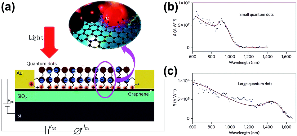
Konstantatos et al. reported an extremely high responsivity (∼107 A W−1) phototransistor based on a PbS QDs/GR composite fabricated via a spin casting combined layer-by-layer approach.63 The schematic of the device and spectral responsivity is shown in Fig. 13. Under illumination, photo-generated electron–hole pairs produced in the PbS QDs, and holes preferred to transfer to graphene; while the electrons remained in the QDs, numerous holes circulated in the channel in graphene, resulting in capacitive coupling and prolonging the carriers' lifetime, and high photoconductive gain was achieved at around 108. The small QDs in the PbS QDs/GR composite possessed higher responsivity than the large sized QDs produced as shown in Fig. 13(b) and (c). The effective electronic coupling of graphene with light-absorbing QDs provides a novel pathway in the applications of optoelectronic devices. Recently, Turyanska et al.59 produced a transistor with higher photoresponsivity of ∼109 A W−1, in which the capped ligands were added to PbS QDs by drop-casting onto the graphene surface. The capped ligands provided a uniform separation of QDs from graphene and maintained its integrity, which served as a dielectric barrier. The accumulation of charge as well as the short transit time of carriers in graphene contributed to the enhancement of photoresponse and photoconductive gain. As a result, the photoresponsivity of the PbS QDs/GR composite can be effectively improved by selecting proper ligands.
 | ||
| Fig. 13 (a) Schematic illustration of a phototransistor based on the PbS QDs/GR composite. Inset: photo-generated electrons and holes prefer to be transferred to graphene. Spectral responsivity of two devices based on small PbS QDs (b) and large PbS QDs (c). Reprinted with permission from ref. 63. Copyright 2012 Macmillan Publishers Limited. | ||
In 2017, Gong et al. fabricated ZnO QDs/GR heterojunction photodetectors by printing QDs directly on a graphene field-effect transistor channel.94 This transistor exhibited a high photoresponsivity of 9.9 × 10⁸ A W−1 with a photoconductive gain of 3.6 × 10⁹ for UV light detection. The figure-of-merit UV detectivity attained 1014 Jones, which was 1 order of magnitude improvement, compared to the best reported nanoscale ZnO-based UV detectors. The clean van der Waals interface mainly takes responsibility for the facilitation of charge transfer from QDs to graphene. The printing quantum devices combined with graphene demonstrated high performance and low cost for its broad prospect in industrialized application.
3.2 Lithium ion batteries
Lithium ion batteries (LIBs), with the advantages of low cost, environmental friendliness and high efficiency, have become one of the most promising energy storage supporters; however, the key factors of high capacity and fast-charging remain to be solved. For the last few decades, the LIBs with anode material based on QDs/GR composites have exhibited excellent performance, which gives this composite significant potential for the LIBs technique. The metal oxide QDs, such as ZnO,28 Fe3O4,29 SnO2,47 CoO69 and V2O5 QDs,95 decorated with graphene or its derivatives have effectively improved the performance of the LIBs.Peng et al. used an ultrasonic method to prepare a CoO QD/GR composite as a LIB anode material.69 The reversible lithium storage capacity reached 1592 mA h g−1 after 50 cycles. The excellent high rate capability and outstanding cycling stability are caused by the large amount of accessible active sites and short diffusion length provided by the CoO QDs. In addition, the Co3O4 QDs/GR composite also achieved a high reversible capacity of 485 mA h g−1 for the rate of 5C.86 Zno–QDs composites are another common metal oxide material used in LIBs. The ALD-grown ZnO QDs/graphene composite achieved a high capacity of 960 mA h g−1 under current density of 100 mA g−1.28 They demonstrated that the electrochemical performance of electrodes can be improved by controlling the particle size and microstructure. The LIB cycle stability can be maintained while the ZnO QD sizes are below 7 nm, and smaller QDs exhibit better rate performance. In 2016, Zhao et al. synthesized the SnO2 QDs@GO composite as the anode material in LIBs, which achieved 1121 mA h g−1 capacity at 100 mA g−1; the volume expansion/contraction was effectively released due to this novel core–shell structure and the graphene reticular structure.47 The good performance mainly resulted from the conductive substrate and stable solid electrolyte interface (SEI) layer. Yao et al. prepared a CoFe2O4 QDs/N-doped GR composite as a LIB anode material by using hydrothermal and calcination methods.96 The CoFe2O4 QDs were 4–12 nm without apparent aggregation on the graphene surface. The manufactured LIBs presented a high initial discharge capacity of 1616 mA h g−1 and reversible capacity of 1223 mA h g−1 after 90 cycles at a current of 100 mA g−1. Those excellent electrochemical properties can be ascribed to the quantum and size effects of CoFe2O4 QDs and the synergetic effect of N-doped graphene.
In particular, the modification of rGO by sulfate groups is an admirable strategy for the reduction reaction, which can avoid the use of toxic agents and thermal treatments. Besides, the sulfate groups can serve as a strong bridge to link nanoparticles and graphene, and promote electron transfer. In 2016, Backert et al. synthesized Ni@Fe2O3 nanoparticles-sulfonated rGO composites as the anode material of LIBs.97 The reversible capacity reached to 1051 mA h g−1 after 40 cycles, which was more than two times higher than that of unwrapped Ni@Fe2O3 (460 mA h g−1).
Due to the small sizes and quantum effects of QDs, QDs/GR composites can be prepared below critical particle size,98 preventing structural collapse during cyclic charge/discharge processes. The reticular structural graphene can buffer its volume expansion/constriction induced in cyclic processes, the excellent graphene conductivity also contributes to quick charge. QDs/GR composites can therefore effectively maintain structural integrity of the active substance, resulting in improving the LIB cyclic stability.
3.3 Solar cells
Solar cells are common photovoltaic devices for producing alternative energy. Numerous research works focus on the conversion efficiency improvement. Fortunately, the QDs/GR composites provide a novel pathway to promote problem solving.In 2014, Parand et al. fabricated a GR/PbS composite as the counter electrode for CdS/CdSe QDs sensitized solar cells (QDSC).85 The maximum conversion efficiency was 2.63%, which was much higher than that of the sole PbS (1.28%) or graphene (0.23%) counter electrode. It is suspected that the GR/PbS electrode provides low charge-transfer resistance in order to enhance its conversion efficiency. In 2016, Kim et al. reported the PbS QDs/GR hybrid, as a sandwich structure including 10 layers of tetrabutylammonium iodide (TBAI)–PbS cQDs incorporated with 9 layers graphene sheets and 2 layers of 1,2-ethanedithiol (EDT)–PbS cQDs deposited on ZnO/ITO/glass substrates, achieved a high conversion efficiency of 9.18%.99 The TBAI and EDT solutions served as the exchange ligand and electron blocking/hole transport layer in solar cells. The schematic diagrams of the device, energy level and electron transfer are shown in Fig. 14(a)–(c), respectively. As shown in Fig. 14(d), the PbS cQDs incorporated with graphene presented an improved photovoltaic performance of 8.82 ± 0.55%. The PL quenching behavior demonstrated that these materials and sandwich structures bring a fast charge extraction from QDs to graphene flakes and the efficiency is enhanced by adding conductive graphene. Eck et al. fabricated bulk heterojunction solar cells based on a CdSe QDs/GR composite.30 The conversion efficiency reached to 4.2%, and the open-circuit voltage was increased by 25–30% with values up to 0.8 V, compared to the QD only based devices. They also confirmed a higher electron mobility and reduction of trapped charges in the solar cell active layer. A rGO/CuInS2 QD hybrid that served as an electron acceptor for polymer-based solar cells was also reported by Meng et al. in 2015.54
 | ||
| Fig. 14 (a) Schematic diagram of a solar cell based on a colloidal PbS QDs/GR composite. (b) Energy level diagram of the as-obtained device. (c) Emission of electrons and recombination in QDs (left), and their transfer to the graphene sheet (right). (d) J–V characteristics of the solar cell based on TBAI–PbS/EDT–PbS (black dotted line) and TBAI–PbS/GR (9 layers)/EDT–PbS (red dotted line) under illumination of sunlight. Reprinted with permission from ref. 99. Copyright 2016 American Chemical Society. | ||
Due to the properties of low cost, high energy conversion, and simple fabrication procedure, dye-sensitized solar cells (DSSCs) have attracted much attention. In 2016, Chang et al. synthesized GQDs@GR foam nanosheets for application of DSSC electrodes.100 The fabricated electrodes had a high energy conversion efficiency of 9.59% with an open-circuit voltage of 0.75 V. The abundant defect sites at the edges of GQDs provided excellent electrocatalytic activity for the reduction of I3−. The high electronic conductivity graphene foam nanosheets act as fast electron transportation channels for promoting the charge transfer from GQDs to the fluorinated tin oxide (FTO) substrate.
Thiol-functionalized rGO attached to QDs also could be applied to active materials in solar cells. In 2016, Madsuha et al. prepared thiol decorated rGO–CdSe QDs and multi-walled carbon nanotubes–CdSe QDs hybrids.101 The fabricated solar cells achieved initial power conversion efficiency values of about 2% under AM1.5G illumination. Due to the decoration with thiol, the binding between the QDs and nanocarbon became stronger, which was beneficial for the preservation of the hybrid nanomorphology.
3.4 Photocatalysis
In the past few decades, photocatalysis has been the subject of extensive research for applications in environmental pollutant removal and solar energy conversion. Semiconductors are usually used as the light-absorption material, and graphene is an excellent charge transfer material for the enhancement of photocatalysis performance.In 2015, Gao et al. used a solvothermal method to prepare a MoS2 QD–GR–TiO2 composite,53 and the photocatalytic performance was demonstrated to be 4 times higher than P25. It was found that the MoS2 QDs served as a co-catalyst, which remarkably increased the visible-light absorbance, charge separation efficiency and enhancement of reaction sites. Meanwhile, a report by Tayyebi et al. indicated that a ZnO QDs/GR composite can enhance the absorption from UV to visible spectra.33 The introduced graphene promoted the absorption intensity and restrained the photocorrosion effect. In 2015, a ZnO@PbS QDs/GO composite applied in suspended photocatalytic H2 evolution was reported for the first time.102 The process of multiple exciton generation (MEG) enhanced the photocatalytic efficiency of hydrogen generation and the separation of electron–hole pairs. It provided a new pathway for QDs/GR composite synthesis with MEG properties. In addition, compared to the pure CdS QDs and graphene sheets, a CdS QDs/GR hybrid, synthesized by the LbL-grown technique, was found to have high photocatalytic activity via UV-visible light spectrometer measurement.32
As is well known, TiO2 is widely used as an industrial photocatalyst, due to its properties of good stability, strong oxidation resistance and low toxicity, but the photo-generated electrons and holes recombine quickly because of its wide band gap. It is therefore a challenge to improve TiO2 performance in photocatalysis application. The GQDs/GO composite combined with TiO2 nanotubes provide a new route to solve this problem. Very recently, Tian et al. prepared N, S co-doped GQDs–rGO–TiO2 nanotube composites by alkaline hydrothermal and physical stirring methods.103 These composites exhibited high photodegradation efficiency that was 1.8 times and 16.3 times higher than those of rGO–TiO2 nanotube composites and pure TiO2 nanotubes, respectively, for the degradation of methyl orange under visible light irradiation (λ > 400 nm). The excellent photocatalytic ability was ascribed to the novel combination of upconversion GQDs and large surface area rGO and TiO2 nanotubes. The N, S co-doped GQDs can effectively suppress electron–hole recombination and extend the range of visible light, due to its upconversion properties, and the large surface area rGO and TiO2 nanotubes can improve charge separation and stabilization. Yang et al. reported the ALD-grown TiO2 QDs/GR composite, which also demonstrated significant photocatalytic enhancement, compared to P25 TiO2 and TiO2 film/GR.104
Halide perovskite QDs have also been developed in photocatalytic applications. In 2017, for the first time, Xu et al. synthesized a perovskite composite CsPbBr3 QDs/GO as a photocatalyst to convert CO2 into solar fuel in nonaqueous media.105 The rate of electron consumption increased by 25.5%, compared to pure CsPbBr3 QDs; due to the GO improved electron extraction and transport, the PL quenching of CsPbBr3 QDs/GO composite demonstrated the electron transfer from QDs to GO. Meanwhile, the CsPbBr3 QDs/GO composite decayed faster than pure CsPbBr3 QDs with the measured average PL decay time decreasing from 38.3 to 11.3 ns.
3.5 Electrochemiluminescence sensors
Owing to the excellent properties of low cost, label-free, and high sensitivity, ECL detection has stimulated significant interest in the preparation of new kinds of materials and exploring the applications.106–108 ECL sensors based on QDs/GR composites have been applied in biomedical detection, the detection of cytochrome C,109 human IgG,110 alpha fetoprotein,111 carbohydrate antigen,112 and chlorinated phenols.34,113,114Normally, the QDs possess poor biocompatibility and low ECL signals, and have limited applications in bioanalyses. The QDs/GR composites provide a novel pathway for this technique by improving the biocompatibility and ECL signals. Wang et al. fabricated an ECL sensor based on the CdSe QDs/GO–chitosan composite to detect cytochrome C.109 The possible ECL mechanisms are as follows:
| CdSe + e− → CdSe˙− | (3) |
| S2O82− + e− → SO42− + SO4˙− | (4) |
| CdSe˙− + SO4˙− → CdSe* + SO42− | (5) |
| CdSe* → CdSe + hν | (6) |
K2S2O8 served as coreactant; the strong oxidant SO4˙− radicals and CdSe˙− anion radicals were produced by the electrochemical reduction of S2O82− and CdSe, respectively. The SO4˙− radicals reacted with CdSe˙− and produced an excited state (CdSe*), this ECL sensor achieved selective ability for cytochrome C from bovine serum albumin and glucose, the long-term stability and high ECL intensity were also great. The porous structure of GO–chitosan promotes the loading of CdSe QDs and provides a large interface for electrode reactions. Besides, in this composite, the GO plays an important role in the generation of ECL signals and improves the stability of radicals and makes the fabrication of SO4˙− and CdSe˙− easier. The excellent conductivity of GO promotes electron transfer from CdSe QDs to the glass carbon disk (GCE) electrode.
In 2013, Yang et al. developed a carbon QDs/GR composite to detect chlorinated phenols.114 The ECL signals were derived from the analytes and carbon QDs with S2O82− serving as co-reactant. This ECL sensor achieved real-time detection of pentachlorophenol with ultrahigh sensitivity of 1.0 × 10⁻¹² M concentration in a range from 1.0 × 10⁻¹² M to 1.0 × 10⁻⁸ M. The eco-friendly and recyclable sensing platform showed ideal recovery rates in real water environments.
3.6 Supercapacitors
Supercapacitors have attracted extensive research for energy storage. However, further improving their power density, cycling stability, charge and discharge rates, and reducing its maintenance cost still present a challenge. Fortunately, graphene is an excellent conductive layer that could improve the supercapacitor performance by increasing the electrical conductivity.The large specific surface area of active composite materials has a significant influence on supercapacitor performances. In 2017, Zhang et al. prepared a GO/carbon dots/polypyrrole composite and used it as an electrode active material.115 In this ternary structure, the carbon dots were sandwiched between GO and the polypyrrole layer, which effectively promoted the electron transport and reduced the resistance. The large specific surface area of carbon dots also enhanced the interfacial properties and increased the dielectric constant of the composite. As a result, the manufactured supercapacitor exhibited a high capacitance of 576 F g−1 at a current density of 0.5 A g−1, and achieved an excellent cycle stability after 5000 cycles. Also, with the consideration of enhancing surface area, Jinlong et al. synthesized a NiMoO4 QDs@nanohole rGO composite that showed better specific capacitance (2327.3 F g−1) and cycling stability, compared to the NiMoO4@rGO composite (1801.2 F g−1).116
Asymmetric supercapacitors (ASC) provide a desirable strategy to improve the performance with fast ion transport. In 2015, Xia et al. synthesized a Fe2O3 QDs/functionalized GR composite as anode material for ASC.117 The fabricated ASC exhibited a high energy density of 50.7 W h kg−1 at a power of 100 W kg−1 and excellent cycling stability. The ionic liquid electrolytes effectively enhanced energy density. In 2016, Shen et al. synthesized a RuO2@C/rGO-based ASC with 1-ethyl-3-methylimidazolium tetrafluoroborate (EMIM-BF4) ionic liquid electrolyte.118 As shown in Fig. 15(a) and (b), the CV and GCD curves present fast charging/discharging capability and good reversibility. The carbon coated RuO2/rGO-based ASC demonstrated higher specific capacitance, compared to the RuO2/rGO-based ASC (Fig. 15(c)). Meanwhile, the ASC showed excellent cycling stability and coulombic efficiency with a capacitance of 47.3 F g−1 under 3.5 V potential windows. It also exhibited 98.5% capacitance retention over 100![[thin space (1/6-em)]](https://www.rsc.org/images/entities/char_2009.gif) 000 cycles and nearly 100% coulombic efficiency at the current density of 3 A g−1 (Fig. 15(d)).
000 cycles and nearly 100% coulombic efficiency at the current density of 3 A g−1 (Fig. 15(d)).
 | ||
| Fig. 15 (a) Cyclic voltammetry (CV) curves and (b) galvanostatic charge/discharge (GCD) curves of the RuO2@C/rGO-based ASC. (c) Specific capacitances of the RuO2@C/rGO and RuO2/rGO-based ASC. (d) Cycling stability and coulombic efficiency of the RuO2@C/rGO-based ASC. Reprinted with permission from ref. 118. Copyright 2016 Royal Society of Chemistry. | ||
Highly transparent and flexible supercapacitors based on QDs/GR composites have attracted lots of research interest, due to great potential for use in portable devices. In 2013, He et al. prepared a 3D GR/MnO2 composite as the active electrode material of a flexible supercapacitor via electrodeposition.119 They achieved a maximum specific capacitance of 465 F g−1 under the optimized MnO2 content of 0.1 mg cm−2 at a scan rate of 2 mV s−1. These excellent performances could mainly be ascribed to the high conductivity and porous structure of graphene, and good contact between graphene and MnO2. In 2016, Lee et al. prepared a GQDs-interdigitated pattern of a graphene (ipGR–GQDs) composite via the electrophoretic deposition method.120 The fabricated supercapacitor exhibited high energy storage (9.09 μF cm−2), stable cycle retention (about 100% for 10000 cycles), high transparency (92.97% at 550 nm), and short relaxation time (8.55 ms). The high stability could be maintained even at a severe bending angle of 45° with 10000 cycles.
3.7 Other applications
QDs/GR composites can also be applied in some emerging applications such as biomarkers,87 drug delivery,121 gas detection,122 Li–O2 batteries,123 sodium ion batteries,124 fuel cells,125,126 electrocatalysts,127 environmental pollutant detection,128,129 photoelectrochemical determination,130–134 etc. QDs/GR hybrids and the QDs/GR composite materials are being further developed, but there are still some drawbacks hindering their extensive applications. The photoelectric responsivity of some QDs/GR hybrids is too low for application in devices, and some photodetectors only present high responsivity in specific narrow wavebands. The performance of QDs/GR-based photodetectors greatly depends on the interfacial states and photogenerated screening field, and therefore, the sensitivity and response time are limited. For solar cells, the conversion efficiency of QDs/GR-based solar cells needs further improvement for industrial applications. Additionally, the cost of manufacturing QD/GR devices is too expensive to meet the large-scale industrial applications. We believe that with the development of scientific research, more QDs/GR composites will be found for application in different fields.4 Summary and prospects
QDs/GR composite materials have attracted much attention due to their excellent effects, and various synthetic methods have been investigated for their fabrication. Herein, we reviewed numerous techniques for QDs decoration on graphene surfaces. With the development of the decoration method, QD/GR composites having multilayer structures were synthesized and widely applied in photodevices. Comparing the different techniques, the proper synthetic methods are highly dependent on the application requirements. Firstly, the hydrothermal/solvothermal method is unsuitable for the synthesis of QD/GRs composites for photodevices because it is hard to control the QDs size by this method. The spin-coating method has huge potential for industrial application, due to the controllability of the film thickness. IBSD and MBE techniques have contributed significantly to QD/GR composite synthesis because they produce ordered and size-tunable QDs. The electrochemical method has been demonstrated to be an environmentally friendly and low-cost technique, which is adaptable for high performance supercapacitor application.The insightful strategies for improving the performance of the devices can be summarized as follows. Firstly, the ligands linked or capped with QDs and graphene provide a suitable pathway to fabricate QDs/GR composites and promote their photoelectric properties. The proper choice of species and ligand lengths is essential for performance improvement. The capped ligands can serve as dielectric barriers and maintain the integrity, leading to accumulation and shortening the transit time, resulting in the enhancement of photoresponse and photoconductivity. Secondly, the combined QDs and graphene multilayer sheets have been shown to be excellent structures and are applicable in phototransistors and solar cells. They exhibit the effective transfer of photogenerated electrons to adjacent graphene, prolonging the lifetime of the carriers. The internal series resistance decreases with the increase of graphene layers and is beneficial for the improvement of device performance. Thirdly, the substrate types of the fabricated devices have a significant impact on their performances. For example, the intrinsic electric field of the PZT substrate can improve the separation of photo–hole pairs in QDs and the formed built-in electric field can promote the holes' transfer from the QDs to the graphene channel. There remain various types of substrates for assembly with QDs/GR composites that are worthy of future investigation.
The QDs in the QDs/GR composite mainly provide an outstanding strategy for high-efficiency exciton dissociation, and graphene mainly acts as a highly efficient charge transport channel. This composite has several advantages as follows: (1) strong quantum effects in zero-dimensional QDs, which yield excellent electronic and optoelectronic properties; (2) the high conductivity of graphene benefits the exciton dissociation and charge transfer at the interface with proper interfacial electronic structures; (3) quantum confinement enhances carrier lifetime, which cooperates with graphene's high carrier mobility to improve the responsivity and photoconductive gain.
Preparing ideal QDs/GR composites with high stability, uniform dispersion, tunable size and excellent performance to meet the industrial requirements is however, still a challenge. The preparation of QDs/GR composites by a convenient, low-cost, and established technique is a research breakthrough. We expect to witness the development of QDs/GR composite materials in the next few decades. We believe these novel composites will change the development of science and technology.
Conflicts of interest
There are no conflicts to declare.Acknowledgements
This work was supported by the National Natural Science Foundation of China (No. 11704330, 11564043 and 11504322), the Applied Basic Research Program of Yunnan Province (No. 2016FB006 and 2015FD006), the Scientific Research Key Fund of Yunnan Provincial Department of Education (No. 2015Z002), Yunnan University Action Plan of Serve the Yunnan Province (No. 2016MS15), the Construction Fund of International Joint Research Center for Optoelectronic and Energy Materials by Yunnan Provincial Department of Finance (No. 2017IB033), and the Open Project of National Laboratory for Infrared Physics, Shanghai Institute of Technical Physics, Chinese Academy of Sciences (No. M201509).References
- C. Wang, S. Y. Ke, J. Yang, W. D. Hu, F. Qiu, R. F. Wang and Y. Yang, Nanotechnology, 2015, 26, 105201 CrossRef CAS PubMed.
- C. Fu, H. Wang, T. Song, L. Zhang, W. Li, B. He, M. Sulaman, S. Yang and B. Zou, Nanotechnology, 2016, 27, 065201 CrossRef PubMed.
- K. T. Early and D. J. Nesbitt, Nano Lett., 2015, 15, 7781–7803 CrossRef CAS PubMed.
- M. Tang, S. Chen, J. Wu, Q. Jiang, K. Kennedy, P. Jurczak, M. Liao, R. Beanland, A. Seeds and H. Liu, IEEE J. Sel. Top. Quantum Electron., 2016, 22, 1–7 CrossRef.
- Y. Li, Y. Wang, C. Chen, A. Pang and M. Wei, Chem, 2012, 18, 11716–11722 CrossRef CAS PubMed.
- W. Yue, M. Lan, G. Zhang, W. Sun, S. Wang and G. Nie, Mater. Sci. Semicond. Process., 2014, 24, 117–125 CrossRef CAS.
- W. Yue and G. Nie, J. Nanosci. Nanotechnol., 2015, 15, 1312–1319 CrossRef CAS PubMed.
- K. Bi, W. Z. Gao, T. Q. Zhang, T. Y. Xu, W. W. Zhai and Y. Zhang, Appl. Mech. Mater., 2013, 321–324, 435–438 CrossRef.
- P. Tománek, S. Changyu, D. Senderáková and M. Hrabovský, Proc. SPIE, 2008, 7138, 71382E CrossRef.
- S. Li, Z. H. Ge, B. P. Zhang, Y. Yao, H. C. Wang, J. Yang, Y. Li, C. Gao and Y. H. Lin, Appl. Surf. Sci., 2016, 384, 272–278 CrossRef CAS.
- S. T. Malak, J. Jung, Y. J. Yoon, M. J. Smith, C. H. Lin, Z. Lin and V. V. Tsukruk, Adv. Opt. Mater., 2016, 4, 608–619 CrossRef CAS.
- N. Qiao, Z. H. Chen, Y. B. Yang, S. D. Liu, Y. C. Wang and H. Ye, IEEE Photonics J., 2016, 8, 1–7 Search PubMed.
- R. Liang, D. Yan, R. Tian, X. Yu, W. Shi, C. Li, M. Wei, D. G. Evans and X. Duan, Chem. Mater., 2014, 26, 2595–2600 CrossRef CAS.
- D. Deng, K. S. Novoselov, Q. Fu, N. Zheng, Z. Tian and X. Bao, Nat. Nanotechnol., 2016, 11, 218–230 CrossRef CAS PubMed.
- K. S. Novoselov, A. K. Geim and S. V. Morozov, Science, 2004, 306, 666–669 CrossRef CAS PubMed.
- F. Bonaccorso, Z. Sun, T. Hasan and A. C. Ferrari, Nat. Photonics, 2010, 4, 611–622 CrossRef CAS.
- F. H. Koppens, T. Mueller, P. Avouris, A. C. Ferrari, M. S. Vitiello and M. Polini, Nat. Nanotechnol., 2014, 9, 780–793 CrossRef CAS PubMed.
- F. Cavallo, R. R. Delgado, M. M. Kelly, J. R. S. Pérez, D. P. Schroeder, H. G. Xing, M. A. Eriksson and M. G. Lagally, ACS Nano, 2014, 8, 10237–10245 CrossRef CAS PubMed.
- X. Geng, L. Niu, Z. Xing, R. Song, G. Liu, M. Sun, G. Cheng, H. Zhong, Z. Liu, Z. Zhang, L. Sun, H. Xu, L. Lu and L. Liu, Adv. Mater., 2010, 22, 638–642 CrossRef CAS PubMed.
- C. X. Guo, H. B. Yang, Z. M. Sheng, Z. S. Lu, Q. L. Song and C. M. Li, Angew. Chem., Int. Ed., 2010, 49, 3014–3017 CrossRef CAS PubMed.
- F. Perreault, A. F. Faria and M. Elimelech, Chem. Soc. Rev., 2015, 44, 5861–5896 RSC.
- Y. Q. Huang, R. J. Zhu, N. Kang, J. Du and H. Q. Xu, Appl. Phys. Lett., 2013, 103, 143119 CrossRef.
- Y. Gromova, A. Alaferdov, S. Rackauskas, V. Ermakov, A. Orlova, V. Maslov, S. Moshkalev, A. Baranov and A. Fedorov, J. Appl. Phys., 2015, 118, 104305 CrossRef.
- T. Yu, F. Wang, Y. Xu, L. Ma, X. Pi and D. Yang, Adv. Mater., 2016, 28, 4912–4919 CrossRef CAS PubMed.
- H. Tetsuka, A. Nagoya and S. I. Tamura, Nanoscale, 2016, 8, 19677–19683 RSC.
- W. Guo, S. Xu, Z. Wu, N. Wang, M. M. Loy and S. Du, Small, 2013, 9, 3031–3036 CrossRef CAS PubMed.
- G. Jiang, Y. Su, M. Li, J. Hu, B. Zhao, Z. Yang and H. Wei, RSC Adv., 2016, 6, 97861–97864 RSC.
- X. Sun, C. Zhou, M. Xie, H. Sun, T. Hu, F. Lu, S. M. Scott, S. M. George and J. Lian, J. Mater. Chem. A, 2014, 2, 7319–7326 CAS.
- S. Zhao, D. Xie, X. Yu, Q. Su, J. Zhang and G. Du, Mater. Lett., 2015, 142, 287–290 CrossRef CAS.
- M. Eck, C. V. Pham, S. Zufle, M. Neukom, M. Sessler, D. Scheunemann, E. Erdem, S. Weber, H. Borchert, B. Ruhstaller and M. Kruger, Phys. Chem. Chem. Phys., 2014, 16, 12251–12260 RSC.
- M. M. Tavakoli, H. Aashuri, A. Simchi and Z. Fan, Phys. Chem. Chem. Phys., 2015, 17, 24412–24419 RSC.
- F. X. Xiao, J. Miao and B. Liu, J. Am. Chem. Soc., 2014, 136, 1559–1569 CrossRef CAS PubMed.
- A. Tayyebi, M. Outokesh, M. Tayebi, A. Shafikhani and S. S. Şengör, J. Alloys Compd., 2016, 663, 738–749 CrossRef CAS.
- D. Jiang, X. Du, Q. Liu, L. Zhou, J. Qian and K. Wang, ACS Appl. Mater. Interfaces, 2015, 7, 3093–3100 CAS.
- E. Aktürk, C. Ataca and S. Ciraci, Appl. Phys. Lett., 2010, 96, 123112 CrossRef.
- J. Y. Hou and S. J. Fonash, Appl. Phys. Lett., 1992, 61, 186–188 CrossRef CAS.
- F. A. Rubinelli, J. Appl. Phys., 1994, 75, 998–1004 CrossRef CAS.
- C. Main, J. H. Zollondz, S. Reynolds, W. Gao, R. Brüggemann and M. J. Rose, J. Appl. Phys., 1999, 85, 296–301 CrossRef CAS.
- F. A. Rubinelli, Thin Solid Films, 2016, 619, 102–111 CrossRef CAS.
- H. Huang, J. Wang, W. Hu, L. Liao, P. Wang, X. Wang, F. Gong, Y. Chen, G. Wu, W. Luo, H. Shen, T. Lin, J. Sun, X. Meng, X. Chen and J. Chu, Nanotechnology, 2016, 27, 445201 CrossRef PubMed.
- M. Khan, M. N. Tahir, S. F. Adil, H. U. Khan, M. R. H. Siddiqui, A. A. Al-warthan and W. Tremel, J. Mater. Chem. A, 2015, 3, 18753–18808 CAS.
- Q. Shi, Y. Cha, Y. Song, J. I. Lee, C. Zhu, X. Li, M. K. Song, D. Du and Y. Lin, Nanoscale, 2016, 8, 15414–15447 RSC.
- C. V. Pham, A. F. Madsuha, T. V. Nguyen and M. Krueger, Synth. Met., 2016, 219, 33–43 CrossRef CAS.
- E. Ciftci, M. N. Rahaman and M. Shumsky, J. Mater. Sci., 2001, 36, 4875–4882 CrossRef CAS.
- J. Cao, Q. Liu, J. Du, L. Yang, M. Wei, M. Gao and J. Yang, J. Mater. Sci.: Mater. Electron., 2016, 28, 2267–2271 CrossRef.
- J. Liu and X. Li, Phys. Lett. A, 2014, 378, 405–407 CrossRef CAS.
- K. Zhao, L. Zhang, R. Xia, Y. Dong, W. Xu, C. Niu, L. He, M. Yan, L. Qu and L. Mai, Small, 2016, 12, 588–594 CrossRef CAS PubMed.
- P. Ye, H. Chen, L. Bu, K. Zhang and H. Rong, Acta Phys. Sin., 2015, 64, 078102 Search PubMed.
- X. Zhang, F. Xu, B. Zhao, X. Ji, Y. Yao, D. Wu, Z. Gao and K. Jiang, Electrochim. Acta, 2014, 133, 615–622 CrossRef CAS.
- R. Huang, L. Wang, Q. Zhang, Z. Chen, Z. Li, D. Pan, B. Zhao, M. Wu, C. M. L. Wu and C. H. Shek, ACS Nano, 2015, 9, 11351–11361 CrossRef CAS PubMed.
- H. Fei, R. Ye, G. Ye, Y. Gong, Z. Peng, X. Fan, E. L. G. Samuel, P. M. Ajayan and J. M. Tour, ACS Nano, 2014, 8, 10837–10843 CrossRef CAS PubMed.
- J. He, Y. Chen, P. Li, F. Fu, Z. Wang and W. Zhang, Electrochim. Acta, 2015, 182, 424–429 CrossRef CAS.
- W. Gao, M. Wang, C. Ran and L. Li, Chem. Commun., 2015, 51, 1709–1712 RSC.
- W. Meng, X. Zhou, Z. Qiu, C. Liu, J. Chen, W. Yue, M. Wang and H. Bi, Carbon, 2016, 96, 532–540 CrossRef CAS.
- R. Atchudan, T. N. Edison, S. Perumal, D. Karthikeyan and Y. R. Lee, J. Photochem. Photobiol., B, 2016, 162, 500–510 CrossRef CAS PubMed.
- D. Shao, X. Sun, M. Xie, H. Sun, F. Lu, S. M. George, J. Lian and S. Sawyer, Mater. Lett., 2013, 112, 165–168 CrossRef CAS.
- Z. Zhang, R. F. Wang, J. Zhang, H. S. Li, J. Zhang, F. Qiu, J. Yang, C. Wang and Y. Yang, Nanotechnology, 2016, 27, 305601 CrossRef CAS PubMed.
- D. I. Son, H. Y. Yang, T. W. Kim and W. I. Park, Composites, Part B, 2015, 69, 154–158 CrossRef CAS.
- L. Turyanska, O. Makarovsky, S. A. Svatek, P. H. Beton, C. J. Mellor, A. Patanè, L. Eaves, N. R. Thomas, M. W. Fay, A. J. Marsden and N. R. Wilson, Adv. Electron. Mater., 2015, 1, 1500062 CrossRef.
- Y. Gao, O. Roslyak, E. Dervishi, N. S. Karan, Y. Ghosh, C. J. Sheehan, F. Wang, G. Gupta, A. Mohite, A. M. Dattelbaum, S. K. Doorn, J. A. Hollingsworth, A. Piryatinski and H. Htoon, Adv. Opt. Mater., 2015, 3, 39–43 CrossRef CAS.
- D. I. Son, H. Y. Yang, T. W. Kim and W. I. Park, Appl. Phys. Lett., 2013, 102, 021105 CrossRef.
- X. Liu, X. Ji, M. Liu, N. Liu, Z. Tao, Q. Dai, L. Wei, C. Li, X. Zhang and B. Wang, ACS Appl. Mater. Interfaces, 2015, 7, 2452–2478 CAS.
- G. Konstantatos, M. Badioli, L. Gaudreau, J. Osmond, M. Bernechea, F. P. Garcia de Arquer, F. Gatti and F. H. Koppens, Nat. Nanotechnol., 2012, 7, 363–368 CrossRef CAS PubMed.
- H. Zhang and Y. T. Zhang, MATEC Web Conf., 2016, 44, 01033 CrossRef.
- Y. Zhang, M. Cao, X. Song, J. Wang, Y. Che, H. Dai, X. Ding, G. Zhang and J. Yao, J. Phys. Chem. C, 2015, 119, 21739–21743 CAS.
- Y. Zhang, X. Song, R. Wang, M. Cao, H. Wang, Y. Che, X. Ding and J. Yao, Nanotechnology, 2015, 26, 335201 CrossRef PubMed.
- R. Wang, Y. Zhang, H. Wang, X. Song, L. Jin and J. Yao, IEEE Photonics J., 2015, 7, 4500706 Search PubMed.
- C. Chen, L. Wang, Y. Liu, Z. Chen, D. Pan, Z. Li, Z. Jiao, P. Hu, C. H. Shek, C. M. Wu, J. K. Lai and M. Wu, Langmuir, 2013, 29, 4111–4118 CrossRef CAS PubMed.
- C. Peng, B. Chen, Y. Qin, S. Yang, C. Li, Y. Zuo, S. Liu and J. Yang, ACS Nano, 2012, 6, 1074–1081 CrossRef CAS PubMed.
- Y. Chen, Q. Wu, Y. Ma, T. Liu, Y. Fan, X. Yang, Z. Zhong, F. Xu, J. Lu and Z. Jiang, Sci. Rep., 2015, 5, 17688 CAS.
- Y. L. Chen, Y. J. Ma, D. D. Chen, W. Q. Wang, K. Ding, Q. Wu, Y. L. Fan, X. J. Yang, Z. Y. Zhong, F. Xu and Z. M. Jiang, Appl. Phys. Lett., 2014, 105, 021104 CrossRef.
- H. Ajlani, R. Othmen, M. Oueslati, A. Cavanna and A. Madouri, J. Vac. Sci. Technol., B: Nanotechnol. Microelectron.: Mater., Process., Meas., Phenom., 2013, 31, 020602 Search PubMed.
- K. Rezgui, R. Othmen, A. Cavanna, H. Ajlani, A. Madouri and M. Oueslati, J. Raman Spectrosc., 2013, 44, 1529–1533 CrossRef CAS.
- X. Tan, Y. Li, X. Li, S. Zhou, L. Fan and S. Yang, Chem. Commun., 2015, 51, 2544–2546 RSC.
- L. Tian, S. Yang, Y. Yang, J. Li, Y. Deng, S. Tian, P. He, G. Ding, X. Xie and Z. Wang, RSC Adv., 2016, 6, 82648–82653 RSC.
- F. Niu, Y. Xu, J. Liu, Z. Song, M. Liu and J. Liu, Electrochim. Acta, 2017, 236, 239–251 CrossRef CAS.
- J. Deng, Q. Lu, H. Li, Y. Zhang and S. Yao, RSC Adv., 2015, 5, 29704–29707 RSC.
- Y. Li, S. Li, Y. Wang, J. Wang, H. Liu, X. Liu, L. Wang, X. Liu, W. Xue and N. Ma, Phys. Chem. Chem. Phys., 2017, 19, 11631–11638 RSC.
- R. Madhu, B. Dinesh, S. M. Chen, R. Saraswathi and V. Mani, RSC Adv., 2015, 5, 54379–54386 RSC.
- C. Zou, B. Yang, D. Bin, J. Wang, S. Li, P. Yang, C. Wang, Y. Shiraishi and Y. Du, J. Colloid Interface Sci., 2017, 488, 135–141 CrossRef CAS PubMed.
- Y. T. Kim, J. H. Han, B. H. Hong and Y. U. Kwon, Adv. Mater., 2010, 22, 515–518 CrossRef CAS PubMed.
- Q. Chen, Y. Hu, C. Hu, H. Cheng, Z. Zhang, H. Shao and L. Qu, Phys. Chem. Chem. Phys., 2014, 16, 19307–19313 RSC.
- M. Jing, C. Wang, H. Hou, Z. Wu, Y. Zhu, Y. Yang, X. Jia, Y. Zhang and X. Ji, J. Power Sources, 2015, 298, 241–248 CrossRef CAS.
- H. Yang, C. Guo, G. H. Guai, Q. Song, S. P. Jiang and C. M. Li, ACS Appl. Mater. Interfaces, 2011, 3, 1940–1945 CAS.
- P. Parand, M. Samadpour, A. Esfandiar and A. I. Zad, ACS Photonics, 2014, 1, 323–330 CrossRef CAS.
- X. Zhou, J. Shi, Y. Liu, Q. Su, J. Zhang and G. Du, Electrochim. Acta, 2014, 143, 175–179 CrossRef CAS.
- Y. Wang, M. Li, Y. Zhu, S. Ge, J. Yu, M. Yan and X. Song, Analyst, 2013, 138, 7112–7118 RSC.
- C. V. Pham, M. Krueger, M. Eck, S. Weber and E. Erdem, Appl. Phys. Lett., 2014, 104, 132102 CrossRef.
- C. V. Pham, S. Repp, R. Thomann, M. Krueger, S. Weber and E. Erdem, Nanoscale, 2016, 8, 9682–9687 RSC.
- Z. Sun, Z. Liu, J. Li, G. A. Tai, S. P. Lau and F. Yan, Adv. Mater., 2012, 24, 5878–5883 CrossRef CAS PubMed.
- L. H. Zeng, M. Z. Wang, H. Hu, B. Nie, Y. Q. Yu, C. Y. Wu, L. Wang, J. G. Hu, C. Xie, F. X. Liang and L. B. Luo, ACS Appl. Mater. Interfaces, 2013, 5, 9362–9366 CAS.
- G. Haider, P. Roy, C. W. Chiang, W. C. Tan, Y. R. Liou, H. T. Chang, C. T. Liang, W. H. Shih and Y. F. Chen, Adv. Funct. Mater., 2016, 26, 620–628 CrossRef CAS.
- B. T. Liu, K. H. Wu and R. H. Lee, Nanoscale Res. Lett., 2016, 11, 388 CrossRef PubMed.
- M. Gong, Q. Liu, B. Cook, B. Kattel, T. Wang, W. L. Chan, D. Ewing, M. Casper, A. Stramel and J. Z. Wu, ACS Nano, 2017, 11, 4114–4123 CrossRef CAS PubMed.
- C. Han, M. Yan, L. Mai, X. Tian, L. Xu, X. Xu, Q. An, Y. Zhao, X. Ma and J. Xie, Nano Energy, 2013, 2, 916–922 CrossRef CAS.
- L. Yao, H. Deng, Q. A. Huang, Q. Su, X. Du and G. Du, J. Alloys Compd., 2017, 693, 929–935 CrossRef CAS.
- G. Backert, B. Oschmann, M. N. Tahir, F. Mueller, I. Lieberwirth, B. Balke, W. Tremel, S. Passerini and R. Zentel, J. Colloid Interface Sci., 2016, 478, 155–163 CrossRef CAS PubMed.
- Z. Ma, T. Li, Y. L. Huang, J. Liu, Y. Zhou and D. Xue, RSC Adv., 2013, 3, 7398–7402 RSC.
- B. S. Kim, D. C. Neo, B. Hou, J. B. Park, Y. Cho, N. Zhang, J. Hong, S. Pak, S. Lee, J. I. Sohn, H. E. Assender, A. A. Watt, S. Cha and J. M. Kim, ACS Appl. Mater. Interfaces, 2016, 8, 13902–13908 CAS.
- Q. Chang, Z. Ma, J. Wang, P. Li, Y. Yan, W. Shi, Q. Chen, Y. Huang and L. Huang, Energy Technol., 2016, 4, 256–262 CrossRef CAS.
- A. F. Madsuha, C. Van Pham, R. Thomann and M. Krueger, Synth. Met., 2016, 222, 34–41 CrossRef CAS.
- X. F. Shi, X. Y. Xia, G. W. Cui, N. Deng, Y. Q. Zhao, L. H. Zhuo and B. Tang, Appl. Catal., B, 2015, 163, 123–128 CrossRef CAS.
- H. Tian, K. Shen, X. Hu, L. Qiao and W. Zheng, J. Alloys Compd., 2017, 691, 369–377 CrossRef CAS.
- L. Yang, L. Jiang, W. Fu, A. W. Weimer, X. Hu and Y. Zhou, Appl. Phys. A, 2017, 123, 416 CrossRef.
- Y. F. Xu, M. Z. Yang, B. X. Chen, X. D. Wang, H. Y. Chen, D. B. Kuang and C. Y. Su, J. Am. Chem. Soc., 2017, 139, 5660–5663 CrossRef CAS PubMed.
- G. Jie, J. Zhang, D. Wang, C. Cheng, H. Y. Chen and J. J. Zhu, Anal. Chem., 2008, 80, 4033–4039 CrossRef CAS PubMed.
- G. Jie, H. Huang, X. Sun and J. J. Zhu, Biosens. Bioelectron., 2008, 23, 1896–1899 CrossRef CAS PubMed.
- P. Bertoncello and R. J. Forster, Biosens. Bioelectron., 2009, 24, 3191–3200 CrossRef CAS PubMed.
- T. Wang, S. Zhang, C. Mao, J. Song, H. Niu, B. Jin and Y. Tian, Biosens. Bioelectron., 2012, 31, 369–375 CrossRef CAS PubMed.
- L. L. Li, K. P. Liu, G. H. Yang, C. M. Wang, J. R. Zhang and J. J. Zhu, Adv. Funct. Mater., 2011, 21, 869–878 CrossRef CAS.
- Z. Guo, T. Hao, J. Duan, S. Wang and D. Wei, Talanta, 2012, 89, 27–32 CrossRef CAS PubMed.
- W. Liu, Y. Zhang, S. Ge, X. Song, J. Huang, M. Yan and J. Yu, Anal. Chim. Acta, 2013, 770, 132–139 CrossRef CAS PubMed.
- J. Liang, S. Yang, S. Luo, C. Liu and Y. Tang, Microchim. Acta, 2013, 181, 759–765 CrossRef.
- S. Yang, J. Liang, S. Luo, C. Liu and Y. Tang, Anal. Chem., 2013, 85, 7720–7725 CrossRef CAS PubMed.
- X. Zhang, J. Wang, J. Liu, J. Wu, H. Chen and H. Bi, Carbon, 2017, 115, 134–146 CrossRef CAS.
- L. Jinlong, Y. Meng and L. Tongxiang, Appl. Surf. Sci., 2017, 419, 624–630 CrossRef.
- H. Xia, C. Hong, B. Li, B. Zhao, Z. Lin, M. Zheng, S. V. Savilov and S. M. Aldoshin, Adv. Funct. Mater., 2015, 25, 627–635 CrossRef CAS.
- B. Shen, X. Zhang, R. Guo, J. Lang, J. Chen and X. Yan, J. Mater. Chem. A, 2016, 4, 8180–8189 CAS.
- Y. He, W. Chen, X. Li, Z. Zhang, J. Fu, C. Zhao and E. Xie, ACS Nano, 2013, 7, 174–182 CrossRef CAS PubMed.
- K. Lee, H. Lee, Y. Shin, Y. Yoon, D. Kim and H. Lee, Nano Energy, 2016, 26, 746–754 CrossRef CAS.
- L. Zhang, S. J. Xiao, L. L. Zheng, Y. F. Li and C. Z. Huang, J. Mater. Chem. B, 2014, 2, 8558–8565 RSC.
- Q. Huang, D. Zeng, H. Li and C. Xie, Nanoscale, 2012, 4, 5651–5658 RSC.
- M. N. Samani, H. D. Lim, S. H. Shishavan, H. K. Kim, Y. Ko, M. S. Kim, S. W. Lee, S. F. K. Bozorg, M. Abbasi, H. U. Guim, D. I. Kim, K. C. Roh, K. Kang and K. B. Kim, J. Mater. Chem. A, 2017, 5, 619–631 Search PubMed.
- Y. Wang, Y. Jin, C. Zhao, Y. Duan, X. He and M. Jia, Mater. Lett., 2017, 191, 169–172 CrossRef CAS.
- M. Fan, C. Zhu, J. Yang and D. Sun, Electrochim. Acta, 2016, 216, 102–109 CrossRef CAS.
- J. Cao, Y. Hu, L. Chen, J. Xu and Z. Chen, Int. J. Hydrogen Energy, 2017, 42, 2931–2942 CrossRef CAS.
- M. Govindhan, B. Mao and A. Chen, Nanoscale, 2016, 8, 1485–1492 RSC.
- O. Adegoke, H. Montaseri, S. A. Nsibande and P. B. C. Forbes, J. Alloys Compd., 2017, 720, 70–78 CrossRef CAS.
- O. Adegoke and P. B. Forbes, Talanta, 2016, 146, 780–788 CrossRef CAS PubMed.
- D. Dutta, S. Chandra, A. K. Swain and D. Bahadur, Anal. Chem., 2014, 86, 5914–5921 CrossRef CAS PubMed.
- Y. Zhu, K. Yan, Y. Liu and J. Zhang, Anal. Chim. Acta, 2015, 884, 29–36 CrossRef CAS PubMed.
- X. Zeng, W. Tu, J. Li, J. Bao and Z. Dai, ACS Appl. Mater. Interfaces, 2014, 6, 16197–16203 CAS.
- R. Wang, K. Yan, F. Wang and J. Zhang, Electrochim. Acta, 2014, 121, 102–108 CrossRef CAS.
- L. Ruiyi, Q. Sili, L. Zhangyi, L. Ling and L. Zaijun, Sens. Actuators, B, 2017, 250, 372–382 CrossRef.
| This journal is © The Royal Society of Chemistry 2017 |