
 Open Access Article
 This Open Access Article is licensed under a
 Creative Commons Attribution 3.0 Unported Licence
Intercalating copper into layered TaS2 van der Waals gaps
Rui Liu†
 ab,
Cong Wang†bc,
Yuanyuan Lia,
Yong Xiea,
Qiang Chena,
Ziyu Chen*a and
Qian Liu*bc
ab,
Cong Wang†bc,
Yuanyuan Lia,
Yong Xiea,
Qiang Chena,
Ziyu Chen*a and
Qian Liu*bc
aKey Laboratory of Micro-nano Measurement-Manipulation and Physics (Ministry of Education), Department of Physics, Beihang University, Beijing 100191, China. E-mail: chenzy@buaa.edu.cn
bNational Center for Nanoscience and Technology, No. 11 Beiyitiao, Zhongguancun, Beijing 100190, China. E-mail: liuq@nanoctr.cn
cThe MOE Key Laboratory of Weak-Light Nonlinear Photonics, TEDA Institute of Applied Physics, Nankai University, Tianjin 300457, China
First published on 3rd October 2017
Abstract
Since graphene was successfully exfoliated, intercalation has been reviewed from bulk materials to two-dimensional counterparts. Here 1T phase Cu–TaS2 was successfully prepared via intercalating Cu into 2D layered TaS2 based on a solution method, which cannot damage the crystal structure of the target material and can realize uniform intercalation with a large amount of dopants. The electrical conductivity of 2D TaS2 intercalated by Cu has an obvious increase compared with 2D TaS2. Considering the peculiar metal–insulator transitions (MITs) of TaS2, our work may provide new opportunities for future superconductor and CDW-based memory devices.
Introduction
Over the past decade, two-dimensional (2D) materials have experienced rapid development due to their novel properties1–3 and applications.4–8 Recently, various methods to modify 2D material properties, including vertical/lateral heterojunctions,9–11 external field tuning,12,13 strain engineering14–16 etc., have attracted enormous attention. Among them, the method of intercalating dissimilar materials into a 2D material interlayer with van der Waals (vdW) gaps has been paid more attention due to its simplicity and flexibility.17 Acerce et al. reported that through intercalating ions (H+, Li+ and Na+), trigonal phase MoS2 (1T-MoS2) was an attractive electrode material when used for a high-performance supercapacitor.18 Voiry et al. demonstrated intercalation into chemically exfoliated WS2 nanosheets, which significantly improves the electrocatalytic activity in the hydrogen evolution reaction (HER).19 In addition, the well-known liquid-based exfoliation method for 2D materials is another successful application of intercalation.1T-TaS2 (tantalum disulfide) is a layered transition metal dichalcogenides (TMDs), in which each layer is composed of Ta atoms surrounded by S atoms in an octahedral arrangement. Since 1T-TaS2 possesses delicate balance between electron–electron and electron–phonon interactions,20,21 it exhibits a series of charge-density-wave (CDW) transitions (from metallic phase to different CDW phases) with a decrease in temperature, including an incommensurate CDW (ICCDW) phase (transition temperature at 550 K), nearly commensurate CDW (NCCDW) phase (transition temperature at 350 K), and commensurate CDW (CCDW) phase (transition temperature at 180 K).22 The rich phase states provide a platform to manipulate physical properties to meet requirements of modern electronic technology. In fact, the many intercalations for bulk TaS2 from organic molecules to inorganic cations/anions have been explored based on iodine vapor transport method and chemical vapor transport (CVT) means.23–26 However, there is no report on intercalating dissimilar materials into 2D TaS2 flakes so far.
In this work, we studied intercalating copper into layered TaS2 vdW gaps by employing the solution-based method with the advantage of low cost and easy to implement in comparison with other methods.27–29 With the help of high-resolution transmission electron microscopy (TEM), energy dispersive spectrometry (EDS) mapping and electron energy loss spectrum (EELS) techniques, we characterized the basic features of intercalated samples, such as lattice constants, crystal structure and elemental composition. The experimental results and analyses indicate that the solution-based method does not change the oxidation state and crystal phase of host materials. What is more, the temperature-dependent CDW transition is preserved. A study on the electrical transport indicates that Cu-intercalated TaS2 has an obvious decrease in electrical resistance.
Experimental
Synthesis of Cu–TaS2
1T-TaS2 flakes were prepared by mechanically exfoliating from 1T-TaS2 crystal with Scotch tape, and then transferred to quartz substrates. Quartz as the substrate is because it would not induce electroless deposition in intercalation reaction. The source material of 10 mM tetrakis(acetonitrile) copper(I) hexafluorophosphate (Sigma-Aldrich) in acetone was added into a three-necked round bottomed flask with a condenser. The sample was immersed into the solution, and then heated the solution to 45 °C. The sample undergoes a disproportionation redox reaction, and then the layered TaS2 intercalated copper was cleaned by hot ethanol.Characterizations
X-ray diffraction (XRD) pattern was performed using D/max 2200Pc. TEM images were taken by a JEM-2100 (JEOL, Japan) operating at an accelerating voltage of 200 kV. EDS was collected by an Oxford nanoanalysis EDS systems. EELS was measured by an FEI Tecnai F20 electron microscope. Atomic force microscopy (AFM, Veeco, Dimension 3100) was used to determine the thickness of thin flakes. Metal electrodes (5 nm Cr/50 nm Au) were made by an electron-beam lithography process. The transport properties were measured on the same device before and after intercalation in a Physical Property Measurement System (PPMS).Results and discussion
The XRD patterns of the out-plane structure of TaS2 before and after intercalation are shown in Fig. 1. To avoid the effects of the organic compound during substrates transfer and large variations in crystallinity between different exfoliated flakes, XRD was performed on the same sample before and after the reaction. For TaS2 before intercalation, all peaks can be indexed by standard PDF card (JCPDS no. 88-1008) of the host materials and amorphous peak around 23° comes from the quartz substrates. For TaS2 after intercalation, neither second phase nor other crystalline impurities are detected, which confirms no existence of Cu (JCPDS no. 04-0836) precipitate. All peaks of intercalated sample shift to lower angles, suggesting an expansion in c lattice. Based on the shifts of (001) peak from 15.011° to 14.836°, we could calculate the c lattice parameter changing from 5.897 Å to 5.966 Å.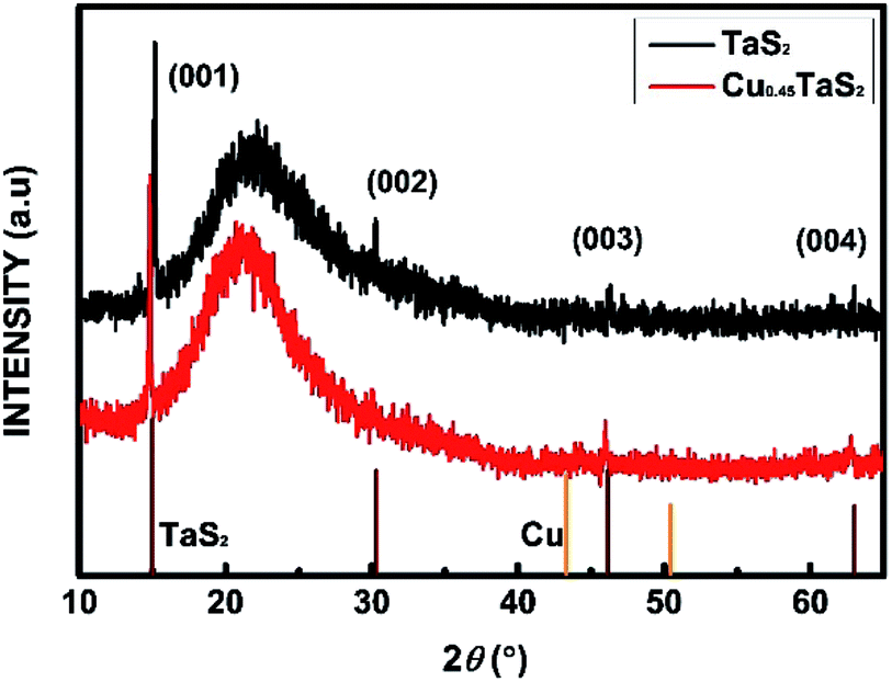 | ||
| Fig. 1 XRD spectra for 1T-TaS2 before and after Cu intercalation. | ||
The details of the in-plane structure and elemental composition were examined by TEM. Fig. 2 shows the TEM images with different Cu concentrations controlled by the reaction time shown in Table 1. The stripe-like phase in Fig. 2(a–d) is due to a charge density wave and periodic lattice distortions.30 The morphology in low dimension and high-resolution TEM (HRTEM) images suggest no aggregate of Cu on the flakes surface. HRTEM, as shown in Fig. 2(e–h), exhibits the flakes still maintain a good crystallization with different Cu content. The EDS was taken to determine the intercalant amount as shown in Fig. 2(i–m). The atom ratio of Ta and S does not change as the Cu concentrations increased from zero (purity) to the highest (13.22% in our results), which illuminates our method is not a substitution of host atoms. Nickel (Ni) laced grids were used in TEM measurement to avoid the effect of Cu on the grids holder.
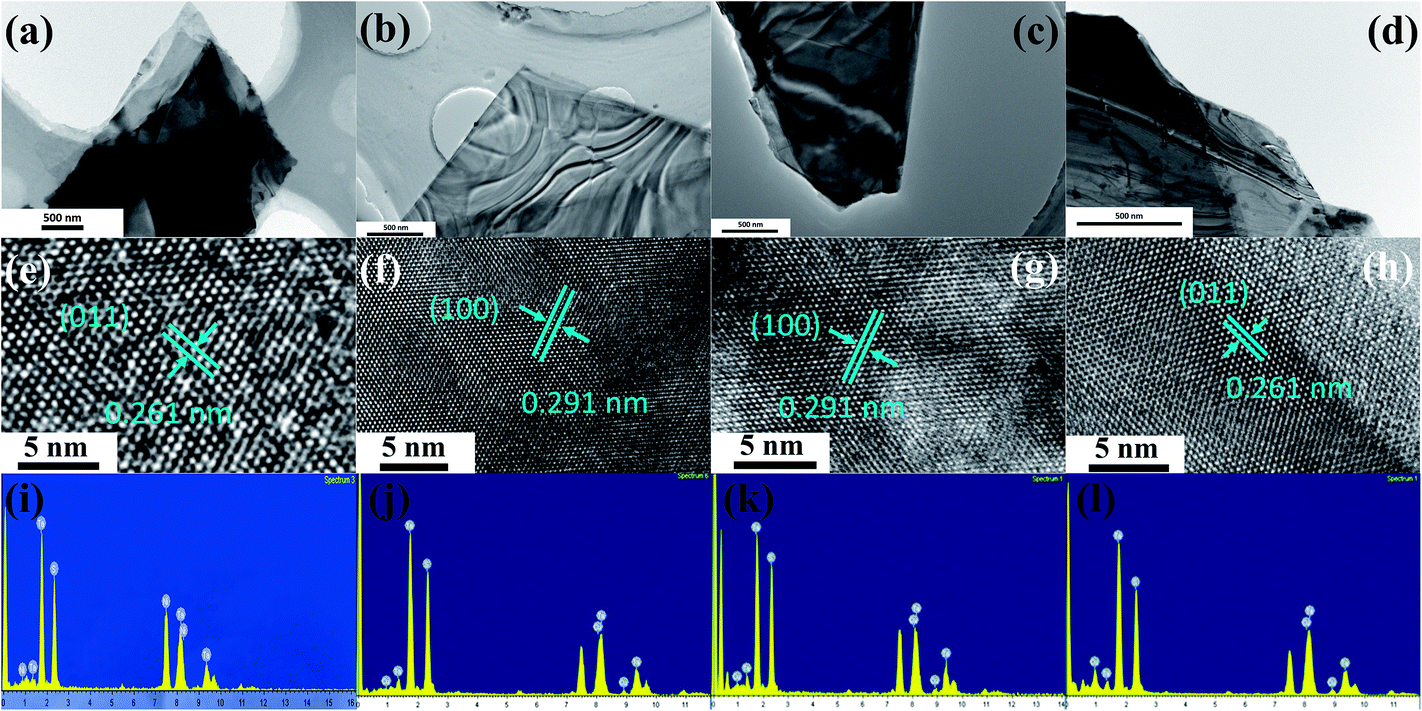 | ||
| Fig. 2 TEM images for materials before and after Cu intercalation with various reaction time: unintercalated, 0.5 h, 2 h, 4 h (a–d), the corresponding HRTEM (e–h), and the EDS spectrums (i–l). | ||
| The reaction time | Atomic percent | Stoichiometry |
|---|---|---|
| 0.5 h | 9.98 | Cu0.32TaS2 |
| 2 h | 11.48 | Cu0.37TaS2 |
| 4 h | 13.22 | Cu0.45TaS2 |
Moreover, when a higher reactant concentration is reached, some aggregated Cu nanoparticles appear on the TaS2 flakes, suggesting an unsuccessful intercalation. In the traditional approach, higher mole ratio creates a higher atoms concentration, which is helpful to improve the doping capacity. However, our results show it is meaningless in improving Cu content for intercalation. This is because copper atoms have little solubility in acetone, leading to that high concentration of atoms and tend to spontaneously assemble to crystal precipitates directly, rather than diffuse to the vdW gaps, while in a low concentration, the atoms prefer to enter the gaps under the action of the thermodynamic driving force.
Fig. 3(a) is our STEM-EDS mapping area with three regions including thick region (A region), a thin region (B region) and background (C region). Mapping results of Ta, S and Cu are shown in Fig. 3(b–d), respectively. Uniform distribution of Ta, S and Cu in A and B regions indicates that three elements have a uniform intercalation. Region A is brighter in intensity than region B. This is because more layers in region A reflected by Fig. 3(b and c) and thus provide more gaps to intercalate Cu shown in Fig. 3(d). According to XRD patterns, HRTEM images and STEM-EDS mapping, it can be confirmed that the Cu have been intercalated into the van der Waals gap of TaS2, as illustrated by schematic diagram (Fig. 4).
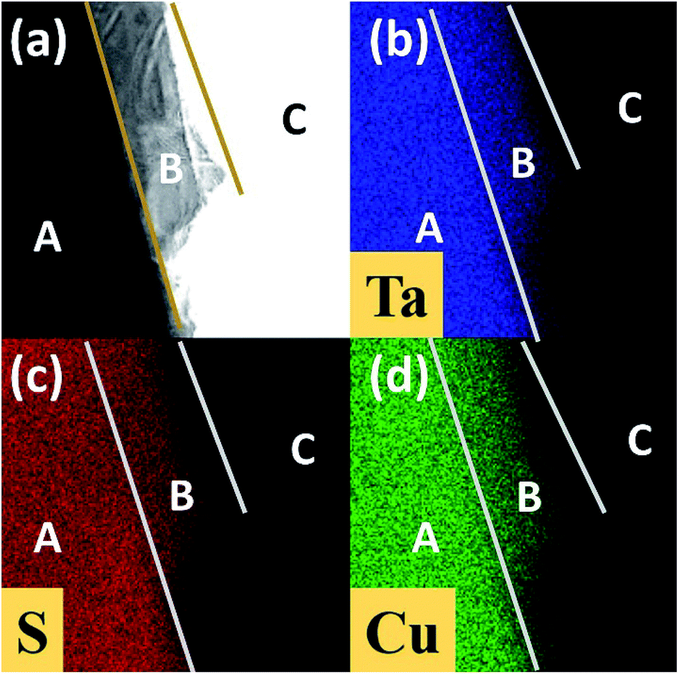 | ||
| Fig. 3 The EDS mappings of elements tantalum, sulphur, and copper. | ||
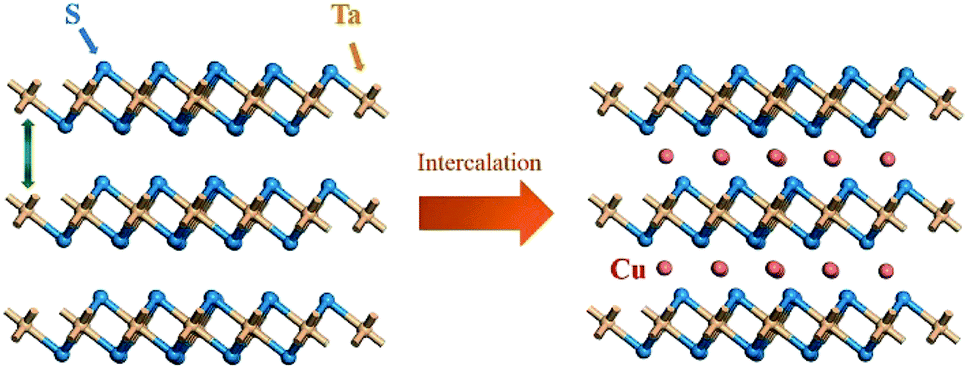 | ||
| Fig. 4 Schematic structure of 1T-TaS2 and Cu–TaS2. | ||
EELS is a powerful tool for identification of the oxidation states of a transition metal by analyzing the near-edge fine structure. The L ionization edges of transition metal always display sharp peaks at near-edge region, which are formed by the transition of an electron from 2p state to unoccupied 3d level. The L2 and L3 indicate the transitions from 2p1/2 to 3d3/2 and 2p3/2 to 3d3/23d5/2, respectively. The intensities come from the unoccupied states in 3d bands.31,32 The L3 and L2 exhibit sharp and intense peak for Cu2+, whereas Cu0 shows broad edges because of full-filled 3d band. The spectrum for Cu–TaS2 has a nearly sharp L3 edge which is similar to Cu2+, but the L2 edge is almost obscured which is closer to copper metal as shown in Fig. 5(a). The L3-to-L2 peak intensity ratio from areas is 3.5 and 1.7 for Cu2+ from CuO and Cu0 from Cu metal, respectively.33 The areas intensity ratio in our spectrum is about 2.48. According to the analysis above, we speculate that the Cu existing state is a mix of Cu2+ and Cu0. Here the shift in Cu L-edge EELS is due to the drift of zero calibration in loss peak.
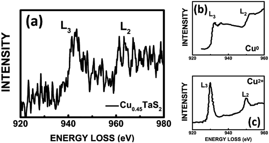 | ||
| Fig. 5 (a) EELS fine structure of copper intercalated into the TaS2 nanoflakes. EELS spectrum of Cu0 (b) and Cu2+ (c) from ref. 31. | ||
The thickness-dependent CDW phase transition has been studied extensively34 for 2D TaS2 without intercalation. When the thickness is down to 24 nm or less, the transition from NCCDW to CCDW state is vanished.35 In order to get a full picture of electrical conductivity with intercalation, the thickness of our device is about 30 nm, shown in the down-left AFM profile of Fig. 6. As shown in Fig. 6, the resistance of the intercalated sample is lower than its pristine state. This is attributed to the increase of charge transfer induced by Cu intercalation, which would lead to an increase in Fermi energy level within host materials. The phase transition behaviors are all preserved, and the transition temperatures are slightly shifts, which should be induced by Cu intercalation. Owing to that the superconducting transition temperature can vary with Cu content in bulk 2H phase CuxTaS2 (0 ≤ x ≤ 0.12),26 implying that Cu-intercalated 2D TaS2 may have a similar property and may provide a new insight in the relationship between CDW phase and superconducting phase.
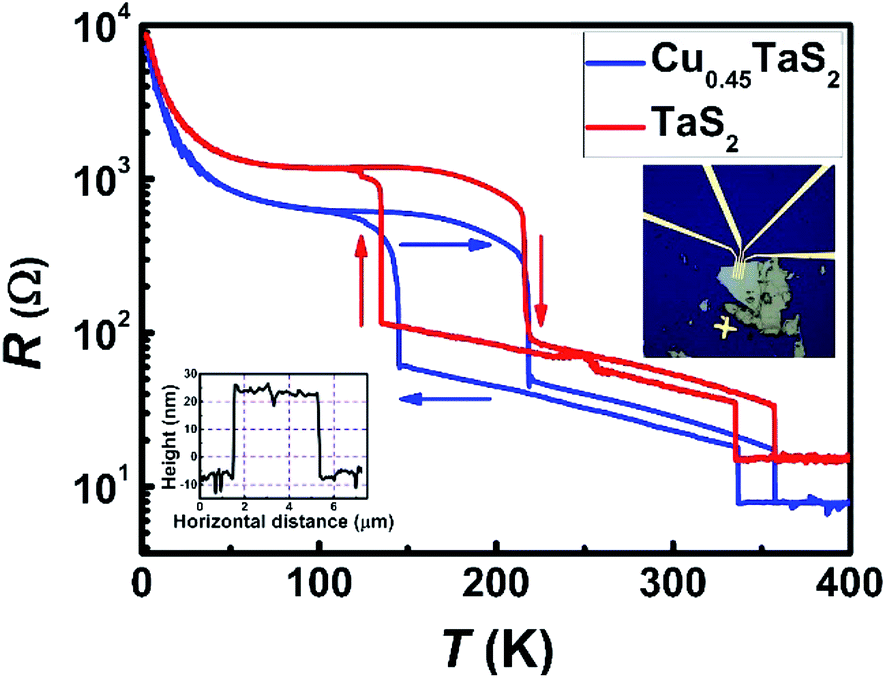 | ||
| Fig. 6 Resistance as a function of temperature for pristine and intercalated samples. The arrows represent the cooling and warming scan directions. (Top right) The optical microscope image of the nano-thick crystal device. (Down left) The AFM profile of the device. | ||
Conclusions
In summary, an efficient method to intercalate copper into 2D layered 1T-TaS2 has been demonstrated. The present method has a higher doping content than the traditional ion intercalation or CVT because of no electrostatic force between atoms. XRD and TEM analyses show that the crystal structure of nanoflake before and after intercalating Cu into TaS2 has not change, benefiting device construction such as heterojunction. The intercalated samples have exhibited a good electrical conductivity even at a thin thickness because of the high carrier density provided by copper. We believe this work might provide a new degree of freedom to explore the unexpected properties in 2D phase transiting materials.Conflicts of interest
There are no conflicts to declare.Acknowledgements
This project is supported by the National Natural Science Foundation of China (11474015, 61227902, 1177040279, 61405223, 51502011, and 10974037), the National Key Research Program of China (2016YFA0200403), and the CAS Strategy Pilot Program (XDA 09020300).Notes and references
- A. K. Geim and K. S. Novoselov, Nat. Mater., 2007, 6, 183–191 CrossRef CAS PubMed.
- H. Zhang, ACS Nano, 2015, 9, 9451–9469 CrossRef CAS PubMed.
- C. L. Tan, X. H. Cao, X. J. Wu, Q. Y. He, J. Yang, X. Zhang, J. Z. Chen, W. Zhao, S. K. Han, G. H. Nam, M. Sindoro and H. Zhang, Chem. Rev., 2017, 117, 6225–6331 CrossRef CAS PubMed.
- F. Bonaccorso, Z. Sun, T. Hasan and A. C. Ferrari, Nat. Photonics, 2010, 4, 611–622 CrossRef CAS.
- D. Chen, L. H. Tang and J. H. Li, Chem. Soc. Rev., 2010, 39, 3157–3180 RSC.
- J. F. Ge, Z. L. Liu, C. H. Liu, C. L. Gao, D. Qian, Q. K. Xue, Y. Liu and J. F. Jia, Nat. Mater., 2015, 14, 285–289 CrossRef CAS PubMed.
- S. X. Yang, C. Wang, C. Ataca, Y. Li, H. Chen, H. Cai, A. Suslu, J. C. Grossman, C. B. Jiang, Q. Liu and S. Tongay, ACS Appl. Mater. Interfaces, 2016, 8, 2533–2539 CAS.
- J. Deng, W. T. Yuan, P. J. Ren, Y. Wang, D. H. Deng, Z. Zhang and X. H. Bao, RSC Adv., 2014, 4, 34733–34738 RSC.
- L. Britnell, R. V. Gorbachev, R. Jalil, B. D. Belle, F. Schedin, A. Mishchenko, T. Georgiou, M. I. Katsnelson, L. Eaves, S. V. Morozov, N. M. R. Peres, J. Leist, A. K. Geim, K. S. Novoselov and L. A. Ponomarenko, Science, 2012, 335, 947–950 CrossRef CAS PubMed.
- A. K. Geim and I. V. Grigorieva, Nature, 2013, 499, 419–425 CrossRef CAS PubMed.
- C. Wang, S. X. Yang, W. Q. Xiong, C. X. Xia, H. Cai, B. Chen, X. T. Wang, X. Z. Zhang, Z. M. Wei, S. Tongay, J. B. Li and Q. Liu, Phys. Chem. Chem. Phys., 2016, 18, 27750–27753 RSC.
- F. Wang, Y. B. Zhang, C. S. Tian, C. Girit, A. Zettl, M. Crommie and Y. R. Shen, Science, 2008, 320, 206–209 CrossRef CAS PubMed.
- Z. Q. Li, E. A. Henriksen, Z. Jiang, Z. Hao, M. C. Martin, P. Kim, H. L. Stormer and D. N. Basov, Nat. Phys., 2008, 4, 532–535 CrossRef CAS.
- J. Feng, X. F. Qian, C. W. Huang and J. Li, Nat. Photonics, 2012, 6, 865–871 CrossRef.
- S. X. Yang, C. Wang, H. Sahin, H. Chen, Y. Li, S. S. Li, A. Suslu, F. M. Peeters, Q. Liu, J. B. Li and S. Tongay, Nano Lett., 2015, 15, 1660–1666 CrossRef CAS PubMed.
- C. Wang, S. X. Yang, H. Cai, C. Ataca, H. Chen, X. Z. Zhang, J. J. Xu, B. Chen, K. D. Wu, H. R. Zhang, L. Q. Liu, J. B. Li, J. C. Grossman, S. Tongay and Q. Liu, Nanoscale, 2016, 8, 5820–5825 RSC.
- J. Y. Wan, S. D. Lacey, J. Q. Dai, W. Z. Bao, M. S. Fuhrer and L. B. Hu, Chem. Soc. Rev., 2016, 45, 6742–6765 RSC.
- M. Acerce, D. Voiry and M. Chhowalla, Nat. Nanotechnol., 2015, 10, 313–318 CrossRef CAS PubMed.
- D. Voiry, H. Yamaguchi, J. W. Li, R. Silva, D. C. B. Alves, T. Fujita, M. W. Chen, T. Asefa, V. B. Shenoy, G. Eda and M. Chhowalla, Nat. Mater., 2013, 12, 850–855 CrossRef CAS PubMed.
- J. J. Kim, W. Yamaguchi, T. Hasegawa and K. Kitazawa, Phys. Rev. Lett., 1994, 73, 2103–2106 CrossRef CAS PubMed.
- F. Zwick, H. Berger and I. Vobornik, et al., Phys. Rev. Lett., 1998, 81, 1058–1061 CrossRef CAS.
- J. A. Wilson, F. J. Di Salvo and S. Mahajan, Adv. Phys., 1975, 24, 117–201 CrossRef CAS.
- X. D. Zhu, Y. P. Sun, X. B. Zhu, X. Luo, B. S. Wang, G. Li, Z. R. Yang, W. H. Song and J. M. Dai, J. Cryst. Growth, 2008, 311, 218–221 CrossRef CAS.
- X. D. Zhu, Y. P. Sun, S. B. Zhang, H. C. Lei, L. J. Li, X. B. Zhu, Z. R. Yang, W. H. Song and J. M. Dai, Solid State Commun., 2009, 149, 1296–1299 CrossRef CAS.
- F. R. Gamble, F. J. DiSalvo and R. A. Klemm, et al., Science, 1970, 168, 568–570 CAS.
- K. E. Wagner, E. Morosan and Y. S. Hor, et al., Phys. Rev. B: Condens. Matter Mater. Phys., 2008, 78, 104520 CrossRef.
- K. J. Koski, J. J. Cha, B. W. Reed, C. D. Wessells, D. S. Kong and Y. Cui, J. Am. Chem. Soc., 2012, 134, 7584–7587 CrossRef CAS PubMed.
- K. J. Koski, C. D. Wessells, B. W. Reed, J. J. Cha, D. S. Kong and Y. Cui, J. Am. Chem. Soc., 2012, 134, 13773–13779 CrossRef CAS PubMed.
- J. P. Motter, K. J. Koski and Y. Cui, Chem. Mater., 2014, 26, 2313–2317 CrossRef CAS.
- R. Hovden, A. W. Tsen, P. Z. Liu, B. H. Savitzky, I. El Baggari, Y. Liu, W. J. Lu, Y. P. Sun, P. Kim, A. N. Pasupathy and L. F. Kourkoutis, Proc. Natl. Acad. Sci. U. S. A., 2016, 113, 11420–11424 CrossRef CAS PubMed.
- D. M. Pease and S. D. Bader, et al., Phys. Lett. A, 1986, 114, 491–494 CrossRef.
- O. L. Krivanek and J. H. Paterson, Ultramicroscopy, 1990, 32, 313–318 CrossRef CAS.
- R. D. Leapman, L. A. Grunes and P. L. Fejes, Phys. Rev. B: Condens. Matter Mater. Phys., 1982, 26, 614–635 CrossRef CAS.
- Y. J. Yu, F. Y. Yang, X. F. Lu, Y. J. Yan, Y. H. Cho, L. G. Ma, X. H. Niu, S. Kim, Y. W. Son, D. L. Feng, S. Y. Li, S. W. Cheong, X. H. Chen and Y. B. Zhang, Nat. Nanotechnol., 2015, 10, 270–276 CrossRef CAS PubMed.
- M. Yoshida, R. Suzuku and Y. Zhang, et al., Sci. Adv., 2015, 1, e1500606 Search PubMed.
Footnote |
| † These authors contributed equally to the work. |
| This journal is © The Royal Society of Chemistry 2017 |