 Open Access Article
Tailoring light emission properties and optoelectronic and optothermal responses from rare earth-doped bismuth oxide for multifunctional light shielding, temperature sensing, and photodetection†
Liumin Fana,
Yang Li*ab,
Xiaohui Lina,
Junhao Penga,
Guifang Ju a,
Shaoan Zhangad,
Li Chena,
Fupo Hec and
Yihua Hu
 *a
*a
aSchool of Physics and Optoelectronic Engineering, Guangdong University of Technology, Guangzhou 510006, China. E-mail: huyh@gdut.edu.cn; lychris@sina.com
bState Key Laboratory of Luminescent Materials and Devices, South China University of Technology, Guangzhou 510640, China
cSchool of Electromechanical Engineering, Guangdong University of Technology, Guangzhou 510006, China
dGuangzhou Maritime University, Guangzhou 510006, China
First published on 19th September 2017
Abstract
Multifunction and high integration has always been a goal worth pursuing when important breakthroughs of multidisciplinary researches in the fields of thermo-luminescent, opto-electronic, photo-magnetic interaction, etc., are emerged. Other significant considerations for a multifunctional strategy proposed in a single-material system are low-cost components and processing, universal applicability, and widespread popularity. Herein, we developed an all-purpose material with a tunable light emission property and controllable optoelectronic and optothermal response process. We showed a disappearance of emission behavior under the excitation of UV light by building a mid-gap host (Bi2O3) along with a rare earth (Sm3+) ion, with multiple energy level configurations, as an emission center. We also demonstrated that this scheme realized the successful imbedding of higher energy level Sm3+ into the conduction band and led to increased current under the excitation of visible light and the depopulated redistribution of the excited state level near the conduction band at higher temperatures. Thus, this phosphor is expected to open up the possibility of potentially free choice of light shielding, temperature sensing, and photodetection in a single-material system.
Introduction
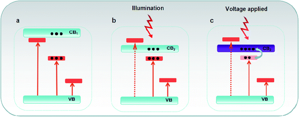
The famous energy band gap (EBG) engineering has often been utilized to design inorganically functional materials. From the plausible crystallographic model, it is possible to customize the spectroscopic feature for a given fluorescent material by employing the EBG theory and engineering route. Typically, the electron migration process of activators along with the related photoluminescence (PL) and photoluminescence excitation (PLE) bands can be tailored via tuning the energy band gap as some transition levels of activators between forbidden bands are invalid when they are deeply embedded into the conduction band (CB) (Fig. 1).1–5 It is noteworthy that the PLE bands of rare-earth or transition metal ions, which are employed in a phosphor as luminescent centers, vary greatly with the forbidden bandwidth of the crystals used as a parent. The controlled use of middle band gap phosphors in combination with a careful choice of suitable activators finds important and widespread applications in the fields of optical shielding and sensing. Moreover, the precisely controlled forbidden bandwidth is also a pivotal determinant of migration performance of activated carriers in the conduction band. A suitable band gap can increase the number of hot and light-activated carriers at room temperature, enhance the migration rate of these carriers in the conduction band (Fig. 1), thus greatly optimize the optoelectronic response process, and open the possibility of designing new multifunctional optoelectronic devices with the integrated characteristics of light shielding, sensing, and detection in a single-material system.In the past few years, numerous materials only featuring single optical or optoelectronic properties have been reported and widely used as a nanothermometer or nanogenerator.6–9 Currently, ZnO has a middle, direct band gap of 3.3 eV, and it has been considered as the superior candidate of a UV sensor and energy harvester; this shows its potential application in a wide range of fields such as in biological and chemical analysis, astronomical studies, flame sensing, and early missile plume detection.10,11 Besides, the optical properties of a Ag2S nanoparticle, carbon dot or rare-doped fluoroscope show relevant temperature dependence in the physiological temperature range; this triggers the application of these materials as nanothermometers for in vivo imaging and hyperthermia treatments.11–19,40
Moreover, short wavelength and high energy can destroy the covalent bonds (e.g., C–H, C–C, and C–Cl) of organic substances and cause incurable damages to cells in the retina of the human eye, which result in serious damages to commonly used organic materials, as well as human health. Therefore, the development of light-shielding materials has attracted significant attention in the field of coatings and sunscreen to reduce the destruction by short-wavelength irradiation. Generally, inorganic light-shielding materials (e.g., TiO2, ZnO, SiO2, and Al2O3) have been widely used owing to their optical and thermal stability as well as nontoxicity. However, their photocatalytic activity as a side effect would simultaneously induce photo-degradation of organic substances. In addition, the application areas of these materials are limited. Therefore, it is necessary to search for novel light-shielding materials with high stability, excellent light-shielding behavior, and multifunction.19,20 It is clear that these kinds of function materials, photon, photo-thermal, and photoelectric interactions are essential. Multifunction and integration are always fascinating; if these characters can be integrated into a single-material system, it will result in a new type of low-cost, multipurpose, and more popular functional materials.
Herein, we developed an integratedly functional material with tunable light emission property and controllable optoelectronic and optothermal response processes by building a mid-gap host along with a Sm3+ ion with multiple energy level configuration as an emission center and realized the potentially free choice of multifunctional light shielding, temperature sensing, and photodetection in a single-material system. The main purpose of this study was to demonstrate the fundamental physical phenomenon in interdisciplinary research, such as in optical, opto-thermal, and opto-electronic multidisciplinary projects.
As a proof-of-concept experiment, top-priority spectroscopic investigation starts from the choice of the host material. Compared with sulfide and selenide, oxide usually has a larger forbidden bandwidth due to its relatively smaller atomic radius although heavy element oxides have enough ability to cover this shortage due to their larger cation radius along with short band gap.21,39 In recent years, significant interest has been generated in research on bismuth trioxide (Bi2O3) due to its unique properties such as middle band gap, high electrical conductivity, and remarkable electron mobility. These properties enable the multifarious applications of Bi2O3 in gas sensor technology and microelectronics and as a photocatalyst and photoanode for dye-sensitized solar cells. Owing to the abundant transition energy level, trivalent lanthanide ions are of great interest for a wide range of applications. The excitation and emission of lanthanides span over the entire spectrum ranging from ultraviolet (UV) to near-infrared (NIR) regions, as determined by the chemical nature of lanthanide ions, except that La3+ and Lu3+ have no luminescence. Herein, Sm3+ ions were employed as representatives of emission center in this material system.
Fig. 1 shows the possible variation in electron transition and migration in a narrower band gap material. The successful imbedding of higher energy-level of activators into the conduction band dominates the overall dynamic behavior of high-energy photon in the Sm-doping Bi2O3 phosphor, including the disappearance of short-wave excitation band, the enhancement of photocurrent under the excitation of visible light, and depopulated redistribution of the excited state near the conduction band at higher temperatures, of the high-energy photon in the Sm-doped Bi2O3 phosphor.
Experimental
Materials
A series of samples Bi2O3:xRe3+ (xRe3+ = 0.3% Sm3+, 1% Nd3+, and 2% Eu3+) was prepared by a conventional solid-state reaction process. The starting materials were Bi2O3 (99.99%), Sm2O3 (99.99%), Nd2O3 (99.99%), and Eu2O3 (99.99%). All chemicals were used directly in an agate mortar and mixed, and then, the mixtures were sintered at 800 °C for 6 h.Characterization
Crystal morphologies of the resulting materials were determined using an X-ray diffractometer equipped with a Cu Kα radiation source (λ = 1.5405 Å) at 36 kV tube voltage and 20 mA tube current. Ultraviolet-visible absorption measurements were conducted via a UV-2450 spectrophotometer (Shimadzu UV-2450, Japan) using BaSO4 as a reference. PL, PLE, and temperature-induced PL spectra were obtained by a high-resolution spectrofluorometer (UK, Edinburgh Instruments, FLS980) equipped with a 500 W xenon lamp as an excitation source. The current–voltage (I–V) curves of the samples under different wavelengths were obtained using a Radiant Technologies Precision premier II Ferroelectric Tester (Albuquerque, NM, USA). To prepare the sample for I–V curve measurements, Bi2O3:xRe3+ (xRe3+ = 0.3% Sm3+, 1% Nd3+, and 2% Eu3+) were pressed into discs with a diameter of 80 mm using a 50 kg press and electroded with silver. To explore the effect of pH on the emission intensity, 0.5 mL of hydrochloric acid (the pH value ranging from 2 to 6), 0.5 mL of sodium hydroxide solution (the pH value ranging from 8 to 12), and 0.5 mL of deionized water were added dropwise to 0.2 g of the Bi2O3:0.3% Sm3+ sample. The mixtures were centrifuged for 10 min in deionized water. In addition, the pH-inducing spectra were obtained using a high-resolution spectrofluorometer (UK, Edinburgh Instruments, FLS980).Results and discussion
Structural analysis
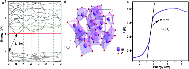
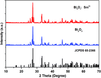
Herein, we have discussed the band gap of the Bi2O3 sample via the theoretical calculation (Fig. 2a). The results show that Bi2O3 semiconductor has a middle, direct band gap of 2.13 eV (more details with respect to the calculation process for theoretical band gap of bismuth oxide are provided in the ESI†). Fig. 2b presents the three-dimensional structure of α-Bi2O3. It crystallizes in the P21/c space group of a known monoclinic phase with the lattice parameters of a = 0.58496(3) nm, b = 0.81648(4) nm, and c = 0.75101(4) nm.21–24 There are two Bi3+ sites (Bi-I and Bi-II) and three O2− sites. The Bi-I atoms and Bi-II atoms consist of six-fold coordination by six O and five-fold coordination by five O, respectively. A six-coordinated Bi3+ and six O2− form a distorted octahedron, which can provide possible non-center symmetrical sites for possible Sm3+ ions. Additionally, the ionic radius of Bi-I ions (1.03 Å) is similar to that of Sm3+ ions (0.958 Å).21,23 Due to the suitable ionic radii, valence state, and crystal structure, Sm3+ can preferentially occupy the sites of Bi-I ions to realize the potential of the Sm3+-doped mid-gap material in the field of multifunctional light shielding, sensing, and detection. XRD data further confirmed the abovementioned structural analysis (Fig. 3). The acquired XRD pattern of Bi2O3:Sm3+ is similar to that of Bi2O3, and all the diffraction peaks of these samples are well indexed to the JCPDS no. 65-2366. The similar crystal structure can also be observed in the XRD data of Bi2O3:Nd3+ and Bi2O3:Eu3+ phosphors (Fig. S1†).To better evaluate the band gap, the experimental diffuse reflectance measurements of Bi2O3 and Bi2O3:Sm3+ phosphor were carried out, and the results converted via the Kubelka–Munk function F(R) (Fig. 2c and S3†). As is known, the correlation between the optical band gap E1 and the absorption coefficient of semiconductor oxides can be described through the following well-known equation:25
| αE ≈ A1(E − E1)m | (1) |
| F(R) = (1 − R)1/2/2R = k/s | (2) |
| [hvF(R)]2 = A2(hv − E1) | (3) |
No emission behavior under the excitation of UV light
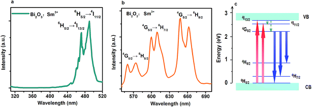
It has been demonstrated that UV light can be successfully absorbed by the Bi2O3:Sm3+ phosphor (Fig. 4); however, Bi2O3:Sm3+ does not exhibit the conventional emission behavior under the excitation of UV light. PL and PLE spectra of the Bi2O3:Sm3+ sample are shown in Fig. 4a and b, respectively. The emission spectra constitute many typical transition bands centered at 560 nm, 609 nm, and 653 nm under 490 nm excitation, which can be ascribed to the electronic transitions of Sm3+ from 4G5/2 to 6H5/2, 6H7/2, and 6H9/2, respectively.27,28 The splitting of typical emission bands is known to be dependent on the crystal field effect, which is caused by the static electric charges in the bismuth-oxide host.29 PLE spectra exhibit the obvious excitation bands peaking at 470 and 490 nm in the visible region of 450–500 nm when monitored under 653 nm emission. They are due to the 6H5/2 → 4I13/2 and 6H5/2 → 4I11/2 transitions of Sm3+. It should be noted that the characteristic excitation band of Sm3+ in Bi2O3:Sm3+ is completely different from that of the material system reported to date. Usually, the excitation bands at 346, 362, 377, 404, and 417 nm can be traced in the PLE spectra of Sm3+-doped NaSrBO3, NaGdF4, and GdVO4.29–31 However, there is no PLE band in the UV regions between 250 nm and 450 nm, as shown in Fig. 4a. The fluorescent decay curves provide the validity of visible excitation as well (Fig. S4†). Therefore, Sm3+ ions can be excited to the 4I13/2 level by 470 nm light, and then, the excited energy relaxes to the 4G5/2 level by non-radiative relaxation. Emission takes place in the transition process between 4G5/2 level and 6H9/2, 6H7/2, and 6H5/2 levels. The higher excitation energy may lead to the delocalization of the excited electron across the conduction band into the vacuum level, and then, this electron finally becomes a free electron (Fig. 4c). A similar optical phenomenon can also be observed in PL and PLE spectra of the Bi2O3:Nd3+ and Bi2O3:Eu3+ phosphors (Fig. S5 and S6†).Optoelectronic detection
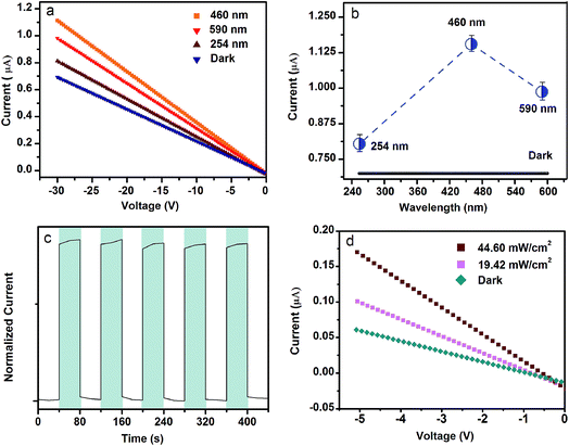
This scheme containing mid-gap host and Sm3+ ions has already proved their potential as a new light-shielding material. The light-controlling current response is another important characteristic. Fig. 5 presents the optoelectronic performance of the Bi2O3:Sm3+ phosphor. The stable I–V curve of Bi2O3:Sm3+ as a function of the bias voltage of 30 V is first shown in Fig. 5a, which is obtained under the excitation of monochromatic light with different wavelengths (254, 460, and 590 nm). The corresponding peak current at a bias of 30 V is plotted as a function of wavelength, as shown in Fig. 5b. The dark current (∼0.70 μA) is found to be lowest, whereas the current under the excitation of 254, 460, and 590 nm light reaches ∼0.81, ∼1.15, and ∼0.99 μA, respectively; this is in accordance with an increase of 15.71%, 64.29%, and 41.43% for the current under the excitation as compared to that of the dark current. The time-dependent optoelectronic response of Bi2O3:Sm3+ exposed to a 460 nm excitation source is depicted in Fig. 5c. The current sharply increases during periodical excitation of light illumination. Furthermore, there are no obvious increases/decreases for the current under illumination in each cycle. The response process is fast, and the corresponding current is stable; this indicates that this material is reliable and repeatable. Fig. 5d presents the result of the I–V measurements with blue illumination. It can be seen that an increase in peak current is achieved by increasing the illumination intensity at a bias of 5 V. Obviously, the current (∼0.10 and ∼0.17 μA) at a fixed illumination intensity of 19.42 and 44.60 mW cm−2 is an order of magnitude (∼66.67% and ∼183.33% times) higher than the dark current (∼0.06 μA). All the investigation about current can be applied to detect the subtle variation in the intensity of the observed light. The similar optoelectronic performance of Bi2O3:Nd3+ phosphors can also be observed in Fig. S8.† Therefore, the material can be used as a calibrated optoelectronic detection material in the required spectral range.Temperature sensing and chemical stability
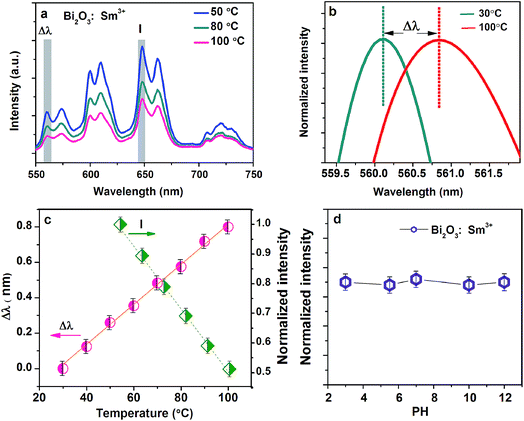
A multifunctional photosensor can extract the information by detecting the variation in emission spectra in an unstable environment. Temperature is a fundamental physical parameter in chemical and biological systems. Therefore, the temperature sensor aims to deliver the knowledge of the local temperature in a given system, which is required for sub-micrometric spatial resolution.6,27,32–35 Fig. 6a shows the PL spectra of the Bi2O3:Sm3+ phosphor excited at 490 nm at different temperatures (50, 80, and 100 °C). The peak intensity monitored at different temperatures ranging from 50 to 100 °C shows a distinct decline. Sm3+ ion presents electronic states very close in energy such that they are thermally coupled. The population distribution in thermally coupled states is strongly temperature dependent as it is governed by Boltzmann statistics. Therefore, any slight modification in the temperature causes relevant modifications in the population of the thermally coupled states.36–38Apart from the temperature-induced population redistribution, temperature-induced spectral shift is also observed in the PL spectra at different treatment temperatures.33,37 Temperature variation leads to modifications in the arrangement of lattice ions surrounding Sm3+ ions. Therefore, crystal field is modificated, which results in a red-shift in the Sm3+ emission lines. The temperature dependency of the intensity ratio at 653 nm emission band and spectra shift between 559 and 562 nm are shown in Fig. 6a and b. The thermal sensitivity is calculated from the experimental data included in Fig. 6c. The value of the error bar is very small, which proves that the results are reliable and the properties of the prepared material are stable. The calculation process is presented in the ESI.† Maximum thermal sensitivity is obtained, and it results from temperature dependence of the intensity and spectral shift being close to 0.98% °C−1 and 1.13% °C−1, respectively, which is larger than the value of thermal sensitivity of green fluorescent protein (0.4% °C−1).36 The similar optothermal performance of the Bi2O3:Eu3+ phosphors can also be observed in Fig. S7.†
In this study, to identify the chemical stability of the as-prepared sample, the intensity variation of emission peak induced by the pH value is investigated in an aqueous environment (Fig. 6d). Obviously, the emission intensity is constant and independent of the pH value. It is inferred that Bi2O3:Sm3+ phosphor is stable under the condition of an acid or alkaline system.
Conclusion
In conclusion, we synthesized a Sm3+-doped Bi2O3 phosphor. The result of theoretical calculation showed that Bi2O3 had a middle, direct band gap of 2.13 eV. We conducted the self-consistent spectroscopic, photoelectric, and optothermal measurements of the representative Bi2O3:Sm3+ phosphor. The excitation spectrum was tailored via the tuning of the band gap. No emission behavior under the excitation of UV light (wavelength < 450 nm) could be observed although distinct emission peak still existed. We also demonstrated the phenomena of temperature-induced population redistribution and temperature-induced spectral shift in the Bi2O3:Sm3+ phosphor. The emission intensity decreased with the increasing temperature, and the red-shift of emission peak at higher temperatures was considered. Maximum thermal sensitivity was attached as well (1.13% °C−1). Moreover, the Bi2O3:Sm3+ sample showed an excellent current response under the excitation of 460 nm and had a linear temperature sensing range with the increasing intensity of the excitation source. Further research on nanocrystallization, which is expected to open up an actual utilization of the as-synthesized phosphor in the visualization of the structural and functional processes in biological living tissue and optical and optoelectronic device, is still in progress.Conflicts of interest
There are no conflicts to declare.Acknowledgements
This work was financially supported by the National Natural Science Foundation of China (Grant No. 51602063, 21671045) and Guangdong Natural Science Foundation (Grant No. 2014A030310444). This work was also supported by the Guangdong High-level personnel of special support program and Open Fund of the State Key Laboratory of Luminescent Materials and Devices (South China University of Technology).References
- L. Sun, Y. Qiu, T. Liu, J. Z. Zhang, S. Dang, J. Feng, Z. Wang, H. Zhang and L. Shi, ACS Appl. Mater. Interfaces, 2013, 5, 9585–9593 CAS.
- W. Shao, G. Chen, A. Kuzmin, H. L. Kutscher, A. Pliss, T. Y. Ohulchanskyy and P. N. Prasad, J. Am. Chem. Soc., 2016, 138, 16192–16195 CrossRef CAS PubMed.
- P. Pust, V. Weiler, C. Hecht, A. Tucks, A. S. Wochnik, A. K. Henss, D. Wiechert, C. Scheu, P. J. Schmidt and W. Schnick, Nat. Mater., 2014, 13, 891–896 CrossRef CAS PubMed.
- Y. Zhuang, J. Ueda, S. Tanabe and P. Dorenbos, J. Mater. Chem. C, 2014, 2, 5502 RSC.
- M. Peng and L. Wondraczek, J. Mater. Chem., 2009, 19, 627–630 RSC.
- L. Lin, G.-Q. Gao, Q. Zhu and A.-W. Xu, J. Mater. Chem. A, 2015, 3, 12845–12851 CAS.
- X. D. Wang, O. S. Wolfbeis and R. J. Meier, Chem. Soc. Rev., 2013, 42, 7834–7869 RSC.
- S. Gu, K. Ding, J. Pan, Z. Shao, J. Mao, X. Zhang and J. Jie, J. Mater. Chem. A, 2017, 5, 11171–11178 CAS.
- M. E. Lee and A. M. Armani, ACS Sensors, 2016, 1, 1251–1255 CrossRef CAS.
- D. Gedamu, I. Paulowicz, S. Kaps, O. Lupan, S. Wille, G. Haidarschin, Y. K. Mishra and R. Adelung, Adv. Mater., 2014, 26, 1541–1550 CrossRef CAS PubMed.
- D. Ruiz, B. Rosal, M. Acebrón, C. Palencia, C. Sun, J. Cabanillas-González, M. López-Haro, A. B. Hungría, D. Jaque and B. H. Juarez, Adv. Funct. Mater., 2017, 27, 1604629 CrossRef.
- D. Jaque and F. Vetrone, Nanoscale, 2012, 4, 4301–4326 RSC.
- H. D. A. Santos, D. Ruiz, G. Lifante, C. Jacinto, B. H. Juarez and D. Jaque, Nanoscale, 2017, 9, 2505–2513 RSC.
- Y. Guo, S. Gu, X. Feng, J. Wang, H. Li, T. Han, Y. Dong, X. Jiang, T. D. James and B. Wang, Chem. Sci., 2014, 5, 4388–4393 RSC.
- E. Hemmer, P. Acosta-Mora, J. Méndez-Ramosb and S. Fischer, J. Mater. Chem. B, 2017, 5, 4365–4392 RSC.
- Q. H. Cui, Y. S. Zhao and J. Yao, Chem. Sci., 2014, 5, 52–57 RSC.
- M. Peng, N. Zhang, L. Wondraczek, J. Qiu, Z. Yang and Q. Zhang, Opt. Express, 2011, 19(21), 20799–20807 CrossRef CAS PubMed.
- M. Peng, J. Qiu, D. Chen, X. Meng and C. Zhu, Opt. Express, 2005, 13(18), 6892–6898 CrossRef CAS PubMed.
- X. Wang, S. Zhou and L. Wu, J. Mater. Chem. C, 2014, 2, 5752–5758 RSC.
- Q. Yu, F. Chen, T. Xu, S. Dai and Q. Zhang, J. Non-Cryst. Solids, 2013, 378, 254–257 CrossRef CAS.
- A. L. J. Pereira, D. Errandonea, A. Beltrán, L. Gracia, O. Gomis, J. A. Sans, B. García-Domene, A. Miquel-Veyrat, F. J. Manjón, A. Muñoz and C. Popescu, J. Phys.: Condens. Matter, 2013, 25, 475402 CrossRef CAS PubMed.
- H. A. Harw, Z. Anorg. Allg. Chem., 1978, 444, 151–166 CrossRef.
- R. D. Shannon, Acta Crystallogr., Sect. A: Cryst. Phys., Diffr., Theor. Gen. Crystallogr., 1976, 32, 751 CrossRef.
- F. Chen, J. Cheng, S. Dai and Q. Nie, J. Non-Cryst. Solids, 2013, 377, 151–154 CrossRef CAS.
- D. Wood and J. Tauc, Phys. Rev. B: Solid State, 1972, 5, 3144–3151 CrossRef.
- A. E. Morales, E. S. Mora and U. Pal, Rev. Mex. Fis., 2007, 53, 18–22 CAS.
- M. Maheshwary, B. P. Singh and R. A. Singh, New J. Chem., 2015, 39, 4494–4507 RSC.
- M. Peng, C. Zollfrank and L. Wondraczek, J. Phys.: Condens. Matter, 2009, 21, 285106–285112 CrossRef PubMed.
- M. Xin, D. Tu, H. Zhu, W. Luo, Z. Liu, P. Huang, R. Li, Y. Cao and X. Chen, J. Mater. Chem. C, 2015, 3, 7286–7293 RSC.
- H. Guan, G. Liu, J. Wang, X. Dong and W. Yu, Dalton Trans., 2014, 43, 10801 RSC.
- Y. Liu, G. Liu, J. Wang, X. Dong and W. Yu, New J. Chem., 2015, 39, 8282–8290 RSC.
- B. Dong, B. Cao, Y. He, Z. Liu, Z. Li and Z. Feng, Adv. Mater., 2012, 24, 1987–1993 CrossRef CAS PubMed.
- J. Feng, K. Tian, D. Hu, S. Wang, S. Li, Y. Zeng, Y. Li and G. Yang, Angew. Chem., Int. Ed., 2011, 50, 8072–8076 CrossRef CAS PubMed.
- H. D. Santos, D. Ruiz, G. Lifante, C. Jacinto, B. H. Juarez and D. Jaque, Nanoscale, 2017, 9, 2505–2513 RSC.
- F. Ye, C. Wu, Y. Jin, Y. H. Chan, X. Zhang and D. T. Chiu, J. Am. Chem. Soc., 2011, 133, 8146–8149 CrossRef CAS PubMed.
- B. del Rosal, E. Ximendes, U. Rocha and D. Jaque, Adv. Opt. Mater., 2017, 5, 1600508 CrossRef.
- Y. Li, M. Gecevicius and J. Qiu, Chem. Soc. Rev., 2016, 45, 2090–2136 RSC.
- F. Menges, P. Mensch, H. Schmid, H. Riel, A. Stemmer and B. Gotsmann, Nat. Commun., 2016, 7, 10874 CrossRef CAS PubMed.
- Y. Li, Y. Li, R. Chen, K. Sharafudeen, S. Zhou, M. Gecevicius, H. Wang, G. Dong, Y. Wu, X. Qin and J. Qiu, NPG Asia Mater., 2015, 7, e180 CrossRef.
- Y. Li, S. Zhou, Y. Li, K. Sharafudeen, Z. Ma, G. Dong, M. Peng and J. Qiu, J. Mater. Chem. C, 2014, 2, 2657–2663 RSC.
Footnote |
| † Electronic supplementary information (ESI) available. See DOI: 10.1039/c7ra08490k |
| This journal is © The Royal Society of Chemistry 2017 |

