
 Open Access Article
 This Open Access Article is licensed under a
 Creative Commons Attribution 3.0 Unported Licence
Passivation of high aspect ratio silicon nanowires by using catalytic chemical vapor deposition for radial heterojunction solar cell application
Gangqiang Dong,
Yurong Zhou *,
Hailong Zhang,
Fengzhen Liu*,
Guangyi Li and
Meifang Zhu
*,
Hailong Zhang,
Fengzhen Liu*,
Guangyi Li and
Meifang Zhu
University of Chinese Academy of Sciences, Beijing 100049, China. E-mail: zhouyurong@ucas.ac.cn; liufz@ucas.ac.cn
First published on 22nd September 2017
Abstract
High aspect ratio silicon nanowires (SiNWs) prepared by metal-assisted chemical etching were passivated by using catalytic chemical vapor deposition (Cat-CVD). Film conformality of hydrogen amorphous silicon (a-Si![[thin space (1/6-em)]](https://www.rsc.org/images/entities/char_2009.gif) :H) deposited by Cat-CVD on SiNWs was investigated and a relationship between the average length of SiNWs and the deposition time of a-Si:H was determined. By optimizing atomic H treatment and a-Si:H deposition on 1 μm length silicon nanowires, a-Si:H/SiNWs radial hetero-junction (RJ-HET) solar cells were fabricated and an efficiency of 16.02% was achieved. Compared with radial homo-junction (RJ-HOMO) solar cells and planar hetero-junction (P-HET) solar cells, the improvements of open circuit voltage and short circuit current of RJ-HET solar cells are discussed based on measurements of capacitance–voltage, dark current–voltage and quantum efficiency. The RJ-HET solar cell based on the SiNW array also shows better omni-directional antireflection properties than the P-HET solar cell.
:H) deposited by Cat-CVD on SiNWs was investigated and a relationship between the average length of SiNWs and the deposition time of a-Si:H was determined. By optimizing atomic H treatment and a-Si:H deposition on 1 μm length silicon nanowires, a-Si:H/SiNWs radial hetero-junction (RJ-HET) solar cells were fabricated and an efficiency of 16.02% was achieved. Compared with radial homo-junction (RJ-HOMO) solar cells and planar hetero-junction (P-HET) solar cells, the improvements of open circuit voltage and short circuit current of RJ-HET solar cells are discussed based on measurements of capacitance–voltage, dark current–voltage and quantum efficiency. The RJ-HET solar cell based on the SiNW array also shows better omni-directional antireflection properties than the P-HET solar cell.
1. Introduction
Radial p–n junction solar cells1,2 based on vertically aligned silicon nanowires (SiNWs) set carrier collection in a direction perpendicular to light absorption. Besides the natural and excellent light-trapping ability of the nanowire structure, radial p–n junctions show an advanced electric collection mode due to a short carrier collection distance, which is beneficial to solar cell performance. Meanwhile, by using the radial p–n junctions, competitive efficiencies can likely be maintained for ultrathin crystalline silicon solar cells when shrinking the volume of silicon and using poor quality silicon absorber. Therefore, more and more studies have been conducted on SiNWs based radial p–n junction solar cells.In 2007, Tian et al.3 first reported a coaxial single SiNW based radial p–i–n solar cell prepared by vapor–liquid–solid technique which obtained a conversion efficiency of 3.4%. After that, with application of lithography and high temperature diffusion4,5 or combination of metal-assisted chemical etching (MACE) and low temperature catalytic shallow doping,6 radial p–n junction concept has been implemented on SiNWs arrays and reported efficiency increased up to >13%. However, the reported performances can still hardly meet people's expectation. On the other hand, the radial junctions are usually in a radial homojunction (RJ-HOMO) status.7,8 The intensified interfacial recombination brought by increased surface area of SiNWs is not well handled. As a result, a common feature of these RJ-HOMO solar cells is the relatively low open circuit voltage (Voc).
Optimized surface passivation is critical to obtain higher efficiency of SiNWs solar cells. In the case of silicon heterojunction solar cells9,10 (abbreviated to HIT, SHJ or HET solar cells), it's well known that c-Si surface is well passivated by hydrogenated amorphous silicon (a-Si:H) thin film and Voc larger than 740 mV can be achieved. Recently, radial heterojunction (RJ-HET) solar cells11–13 with a-Si:H thin films functioned as passivation layer and emitter were successfully fabricated on MACE SiNWs. Plasma enhanced chemical vapor deposition (PECVD), a mature thin film deposition technology widely used in commercial industry, is commonly adopted to deposit silicon thin films. Reported Voc and conversion efficiency of RJ-HET solar cells continuously improved and exceeded RJ-HOMO solar cells14,15 in a short time. However, interface and growth layers have to experience ion bombardment during PECVD process, thus surface damage is unavoidable. And, conformal coverage of small surface features with high aspect ratio is hard to accomplish due to the correlation between surface morphology and local potential field.16 For this reason, PECVD cannot provide good interface passivation for MACE SiNWs with high aspect ratio (usually >10) and large density.
Catalytic chemical vapor deposition (Cat-CVD),17 also called hot wire CVD (HWCVD), is greatly different form PECVD technology. In Cat-CVD, reactive gases (e.g. silane and hydrogen) are catalytically dissociated on surface of heated filament with very high efficiency. The merits of Cat-CVD18–20 are conformal coverage of thin film on small objects, out of surface damage caused by ion bombardment and large amount of atomic hydrogen. Compared with PECVD, Cat-CVD can provide better surface passivation which leads to less shunts at the a-Si:H/SiNWs interface. And, film deposition process of Cat-CVD with plasma-free is easier to control than PECVD. Cat-CVD has been used to create many novel thin films and devices (e.g. SiNx:H passivation layer in multi-crystalline Si solar cells, polymer materials serving as water vapor barrier layers, thin film silicon solar cells, HIT solar cells etc.) and it is gradually developed for wider application for commercial implements.16,17,21
In this paper, a-Si:H shells were deposited by Cat-CVD technology on surface of MACE SiNWs to construct a-Si:H/SiNWs RJ-HET solar cells. According to the SiNWs with varied lengths, conformality and passivation effect of a-Si:H layers were investigated. Conversion efficiency >16% was achieved for a-Si:H/SiNWs RJ-HET solar cells. Performance of a-Si:H/SiNWs RJ-HET solar cells are presented with discussion of interface passivation quality, possible radial transport of carriers and light trapping in omnidirectional angle.
2. Experimental details
Polished (100) oriented silicon wafers (p-type, resistivity 1–3 Ω cm) were used in this work to investigate passivation properties and construct RJ-HET solar cells. The wafers were cleaned in ethanol for 10 minutes and acetone for 5 minutes in an ultrasonic machine at room temperature. Then the wafers were dipped into 2% HF solution for 1 minute to remove native oxide layer. After this, the cleaned silicon wafers were immersed into an aqueous solution which containing 5 mol L−1 HF and 0.02 mol L−1 AgNO3 to prepare SiNWs array. After etching, the as-prepared samples were rinsed copiously in deionized water and then dipped into a NH3·H2O:H2O2 (v/v = 3:1) solution for 5 minutes to remove the Ag layer which wrapped on SiNWs arrays. In the end, the SiNWs samples went through standard RCA clean procedure.
The schematic diagram of fabricated RJ-HET solar cells is shown in Fig. 1. After thermal evaporation of aluminum on rear surface, thermal oxidation was processed at 930 °C with mixed gases of N2 and O2 for 1 hour to form the Al back surface field (BSF). Then, 10% HF solution was used to remove oxide layer of front surface. Before depositing intrinsic passivation layer (i a-Si:H) and phosphorus doped emitter (n a-Si:H), atomic hydrogen treatments were proceeded in Cat-CVD chamber for 60 seconds. The temperatures of the hot filaments (Ta wires, 0.5 mm diameter) and the substrate were kept at 1750 °C and 150 °C, respectively. Other parameters are listed in Table 1.
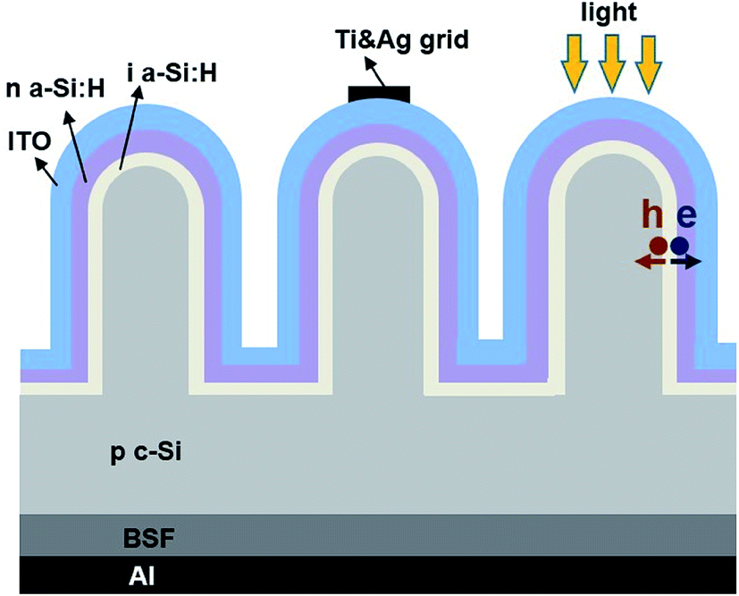 | ||
| Fig. 1 Cross-section schematic of RJ-HET solar cell. | ||
:H thin films deposition by Cat-CVD
| Process | H2 (sccm) | SiH4 (sccm) | PH3 (sccm) | Pressure (Pa) |
|---|---|---|---|---|
| Atomic H treatment | 20 | — | — | 10 |
| i a-Si:H deposition | 3 | 1 | — | 2 |
| n a-Si:H deposition | 3 | 1 | 0.02 | 1 |
After the formation of a-Si:H/SiNWs hetero-junction, a 120 nm ITO layer (40 Ω □−1) was deposited by reactive evaporation in a deposition rate of 0.5 nm s−1 on top of the solar cell to make electrical contacts. The top grid was prepared by Ti and Ag evaporation and the back electrode was formed by Al evaporation.
A conventional planar hetero-junction (P-HET) solar cell was prepared on polished wafer under the same procedure as RJ-HET solar cell. A RJ-HOMO solar cell was prepared on SiNWs by low temperature catalytic shallow diffusion technology6 carried out in the Cat-CVD chamber under a substrate temperature of 250 °C. H2-diluted PH3 (0.5%) was used as the doping gas. After a 25 min doping, a junction depth of about 10 nm can be formed and a radial-homojunction structure can be obtained on the SiNWs. The P-HET and P-HET solar cells were set as comparison samples.
The surface morphologies of a-Si:H/SiNWs samples were observed by using scanning electron microscope (Hitachi S-4800). The minority carrier lifetime was measured by Semilab WT-1200. The measurement of capacitance–voltage (C–V) was carried out on a computer-controlled HP4192A impedance analyzer at 1 MHz fixed frequency with AC voltage of 10 mV. The illuminated current density–voltage characterization of the solar cells was measured under AM1.5 (100 mW cm−2, at 25 °C) illumination.
3. Results and discussion
3.1 Conformality of a-Si![[thin space (1/6-em)]](https://www.rsc.org/images/entities/h3_char_2009.gif) :H layer deposited onto SiNWs by Cat-CVD
:H layer deposited onto SiNWs by Cat-CVD
The conformal coverage of a-Si:H thin film onto SiNWs array plays an essential role of reducing surface recombination and forming good radial pn junctions with fewer shunts. In Fig. 2, SEM images of SiNWs arrays with varied average length after a-Si:H film deposition with different thickness are shown. Before the a-Si:H deposition, atomic H treatments were carried out for about 60 s. Compare Fig. 2(a) and (b), of which share the same 50 s of a-Si:H deposition time, the 1 μm-length SiNWs sample shows a better uniform coating of a-Si:H along the nanowires than the 500 nm-length nanowires. The 500 nm-length SiNWs sample presents wider diameter on top of nanowires. From these we know that 20 nm thick (50 s deposition) a-Si:H is optimal for 1 μm-length SiNWs sample, meanwhile, the 50 s of a-Si:H deposition time is over long for 500 nm-length nanowires. It must be pointed out that the thickness we mentioned here refers to the thickness of a-Si:H deposited on polished Si wafer at the same condition. Due to much larger surface area of SiNWs, under the same deposition condition, a-Si:H thin film is much thinner on SiNWs than on flat Si wafer.
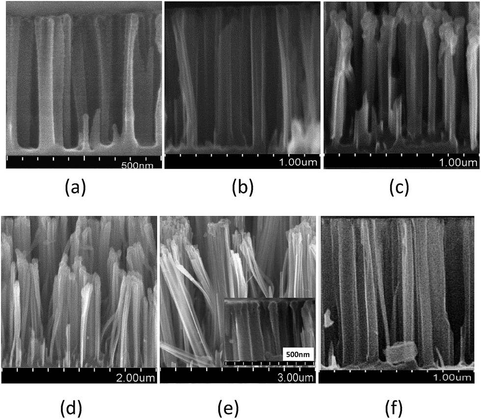 | ||
| Fig. 2 Cross-sectional SEM images of a-Si:H/SiNWs with varied average length of SiNWs and different thickness of a-Si:H thin films. Different thickness was obtained by controlling the deposition time. The combination of average length of SiNWs and thickness (or deposition time) of a-Si:H is (a) 500 nm and 20 nm (50 s), (b) 1 μm and 20 nm (50 s), (c) 1 μm and 60 nm (150 s), (d) 2 μm and 60 nm (150 s) and (e) 3 μm and 60 nm (150 s). A high magnified image of top of nanowires is attached in (e). The deposition pressure of a-Si:H was fixed at 2 Pa. A cross-sectional SEM image of 1 μm-length SiNWs without a-Si:H coating is shown as a reference in (f). | ||
When a-Si:H deposition time extends up to 150 s (60 nm thickness) for 1 μm-length SiNWs, thicker layer of a-Si:H is accumulated on top of nanowires and forms many “fat heads”, as shown in Fig. 2(c). If we solely increase the average length of SiNWs to 2 μm (Fig. 2(d)) and 3 μm (Fig. 2(e)), those “fat heads” gradually shrink.
The above phenomena indicate that, in order to realize conformal coverage of a-Si:H on nanowires, there is an optimal combination of a-Si:H thickness and average length of nanowires. Thicker a-Si film (or longer deposition time) is needed for longer nanowires to form uniform coating and vice versa. When deposition time (or thickness) of a-Si:H and average length of SiNWs match, conformal cover can be realized, as Fig. 2(b) shows. This phenomenon also proves that during Cat-CVD process which has plenty of atomic H in the gas phase, adsorbed radicals diffuse22 along hydride terminated surface of nanowires. In the high magnified image in Fig. 2(e), thin neck just under small “head” of each nanowire can be determined. This is probably due to the radicals depletion caused by long distance diffusion toward the bottom of nanowire. However, once side wall of SiNWs covered by a-Si:H thin film, long distance diffusion will be disturbed by increased surface roughness, and then “fat heads” appear due to the shadow effect as Fig. 2(c) shows.23
It's worth noting that radials may not reach the bottom of long SiNWs at relatively low substrate temperature (150 °C). Furthermore, bending and aggregating appear on nanowires with excess length, which increases difficulties of uniform coating of a-Si:H. Although long nanowires are good for light absorption, with the comprehensive consideration of conformality of a-Si:H layer, 1 μm-length SiNWs were finally chosen to prepare solar cells. In this case, when the thickness of a-Si:H is in range of 20 nm and 60 nm, fairly conformal coverage can be achieved. Now, a nice passivation characteristic of a-Si:H/SiNWs interface is possible. As we expected, after the a-Si:H deposition for about 50 nm, effective minority carrier lifetime (τeff) of the 1 μm-length SiNWs sample is effectively improved from 80 μs (as-cleaned) to 160 μs. Furthermore, radial transportation and collection of carriers can be realized by depositing an ITO layer on SiNWs.
3.2 Optimization of the RJ-HET solar cells
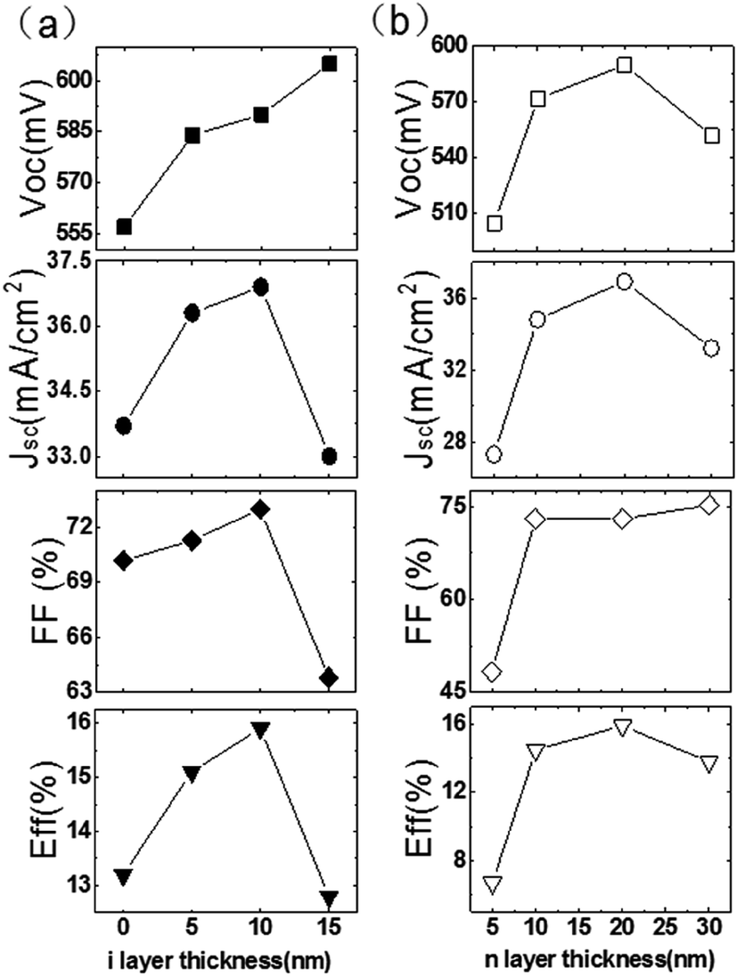
In this work, intrinsic a-Si:H thin film deposited by Cat-CVD functioned as passivation layer and n type a-Si:H thin film deposited by Cat-CVD functioned as emitter layer. Taking into account of the total thickness of a-Si:H required by conformal cover, two series of RJ-HET solar cells with the structure of grid/ITO/n a-Si:H/i a-Si:H/p c-Si/Al were fabricated to optimize the thickness of intrinsic and n type a-Si:H thin films, respectively. In series 1, thickness of n type a-Si:H was fixed at 20 nm and thickness of intrinsic a-Si:H was varied from 0 to 15 nm. The illuminated I–V data including open circuit voltage (Voc), short circuit current density (Jsc), fill factor (FF) and efficiency (EFF) of samples in series 1 are plotted in Fig. 3(a). Voc rises monotonically with the thickness of intrinsic a-Si:H, which indicates that thicker i a-Si:H coverage, less shunts. When i a-Si:H is above 10 nm, Jsc and FF start to decrease due to light absorption and carriers recombination in the intrinsic a-Si:H layer. In series 2, thickness of intrinsic a-Si:H was fixed at optimized value of 10 nm and thickness of n type a-Si:H was tuned from 5 nm to 30 nm. The light I–V data of samples of series 2 are plotted in Fig. 3(b) and the optimized thickness of n a-Si:H is 20 nm. The optimal overall thickness of the intrinsic and n type a-Si:H is around 30 nm, which is consistent with previous SEM measurements. Usually, the overall thickness of a-Si:H layers is 10–15 nm on flat substrate. However, thicker a-Si:H layers (determined from flat surface condition) are needed to realize optimal conformal coverage of SiNWs with enlarged surface area. Finally, a highest efficiency of 15.9% was achieved for the two series of RJ-HET solar cells.
 | ||
| Fig. 3 Light I–V data of RJ-HET solar cells with the structure of grid/ITO/n a-Si:H/i a-Si:H/p c-Si/Al. (a) Series 1 with tuned thickness of intrinsic a-Si:H layer. (b) Series 2 with tuned thickness of n type a-Si:H layer. | ||
3.3 Comparation of the solar cells with different structures
To further understand the passivation effect of Cat-CVD on nanostructure, solar cells with different structures, including P-HET, RJ-HOMO and RJ-HET, were fabricated and compared. Besides c-Si substrate, back and front contacts went though the same fabrication process and optimized deposition condition was adopted for intrinsic a-Si:H layer for all solar cells. The highest light I–V data of each solar cell structures are summarized in Table 2. P-HET solar cell has the highest Voc. Voc of RJ-HET solar cell is 12 mV lower than P-HET solar cell, but 69 mV higher than RJ-HOMO solar cell. Since RJ-HOMO soalr cell and RJ-HET solar cell are both based on 1μm-length SiNWs, they have similar Jsc which is much higher than P-HET solar cell. RJ-HET solar cell has the highest efficiency of 16.02% of these three structures.
| Voc (mV) | Jsc (mA cm−2) | FF (%) | EFF (%) | |
|---|---|---|---|---|
| P-HET | 606 | 29.42 | 76.75 | 13.68 |
| RJ-HOMO | 525 | 36.61 | 73.13 | 14.05 |
| RJ-HET | 594 | 36.98 | 72.93 | 16.02 |
For better understand of interface properties of these solar cell structures, capacitance vs. voltage (C–V) and dark J–V measurements were carried out for P-HET, RJ-HOMO and RJ-HET solar cells. Fig. 4(a) shows the relationship of W2 (W, depletion region width) and V which were re-plotted from the C–V measurements in reverse bias condition. The magnitude of effective density of localized gap states of the interface layer (NI) can be estimated from the slope of W2–V curves.24 It can be seen that P-HET solar cell has the smallest NI due to good passivation of interface. Both RJ-HOMO and RJ-HET solar cells present higher NI than P-HET, which can be assigned to larger surface area induced by SiNWs. NI of RJ-HET solar cell is one magnitude lower than RJ-HOMO solar cell, which confirms the benefits of a-Si:H/c-Si heterojunction structure.
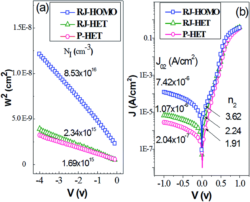 | ||
| Fig. 4 Square of width of the depletion region as a function of voltage obtained from the C–V measurement (a) and dark J–V characteristics (b) of these three solar cells. Effective density of localized gap states (NI), diode quality factor (n2) and saturation current density (J02) of these three solar cells are given in the figures. | ||
Dark J–V characteristics of these three types of solar cells are depicted in Fig. 4(b). The diode quality factor n2 and the saturation current density J02 were fitted from the dark J–V curves in the forward voltage region of 0.15 < V < 0.3 V based on the double diode model.25 RJ-HOMO solar cell has the highest n2 (3.62) and J02 (7.42 × 10⁻⁶ A cm−2), which is probably due to serious surface recombination. In comparison, n2 is reduced to 2.24 and J02 is reduced to 1.07 × 10⁻⁶ A cm−2 for the RJ-HET solar cell also fabricated with SiNWs wafer. Similar phenomenon can be observed in reverse voltage region of dark J–V curves. RJ-HOMO solar cell has the highest leakage current density, while leakage current density of RJ-HET solar cell is much lower.
Both C–V measurements and dark J–V characteristics indicate that interface condition of RJ-HET structure is much better than that of RJ-HOMO structure. In RJ-HET solar cell, lower density of defects states in energy band gap lead to decreased recombination and higher Voc. According to the average data of the light I–V of around 5 parallel samples, Voc of RJ-HET solar cells (581 ± 13 mV) increased by about 50 mV compared with that of RJ-HOMO solar cells (530 ± 15 mV). P-HET solar cells have the best interface condition and the highest Voc (596 ± 10 mV) as expected, mainly due to the smooth interface and good a-Si:H passivation by Cat-CVD.
From Table 2, Jsc of SiNWs solar cells (RJ-HET and RJ-HOMO) increases 24–25% compared with that of the P-HET solar cell. Excellent light trapping effect of the SiNWs structure contributes to higher Jsc. However, average reflectance (350–1000 nm) of ITO covered SiNWs is 8.1% and ITO covered polished c-Si is 16.6%. So, decrease of average reflectance caused by the SiNWs structure is not the only factor that make Jsc increase of 24–25%.
For radial junction SiNWs solar cells, functions of radial transport and collection of photogenerated carriers need to be considered as well. Fig. 5 depicts the internal quantum efficiency (IQE) of RJ-HET and P-HET solar cells. It can be seen that IQE of RJ-HET solar cell is higher than that of P-HET solar cell within the short wavelength range (400–600 nm). It's known that short-wavelength incident light is mainly absorbed by SiNWs in RJ-HET solar cell. When wavelength <450 nm, absorption length is around 1 μm in c-Si. Since average diameter of SiNWs (dozens of nanometer) is much less than the diffusion length of minority carries, photogenerated carriers can be collected rapidly in radial junctions of SiNWs solar cell, thus the short wavelength range of IQE increases in the RJ-HET solar cell. In the range of medium and long wavelength, IQE of RJ-HET solar cell is a little bit lower than that of P-HET solar cell, which may be related to differences of bulk and rear surface recombination.
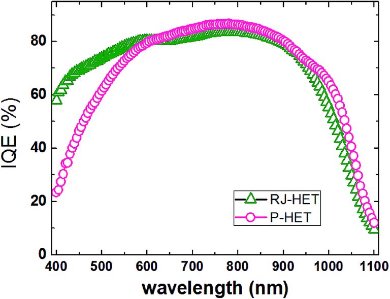 | ||
| Fig. 5 IQE of RJ-HET and P-HET solar cells. The RJ-HET solar cell exhibits an enhanced short wavelength range spectral response, which confirms the validity and superiority of carrier collection in radial junctions. | ||
Nanostructures acting as light trapping layer exhibit a superior antireflection characteristic, i.e. omnidirectionality.26–28 It's of great benefit to photovoltaic application if solar cell has the omnidirectionality. To exam omnidirectional antireflection properties of RJ-HET and P-HET solar cells, angular-dependences of Voc, Jsc, FF, and apparent EFF were measured and compared as shown in Fig. 6. The experimental measured apparent efficiency describes the electrical output of the solar cell under different incident angle of the light. For P-HET solar cell, shown in Fig. 6(b), the light I–V data strongly depend on the angle of incident (AOI). Jsc, Voc and apparent EFF decrease rapidly with AOI increasing. Compared to normal incidence condition, Jsc reduces by 11.9% and 21.9% as AOI changes to be 30°and 60°. Loss of Jsc leads to low apparent EFF for the P-HET solar cell at large AOI conditions. In comparison, RJ-HET solar cell exhibits a better antireflection property over a wide AOI range. Light trapping effect of SiNWs arrays is correlated with incident light random scattering. Scattered and redirected light can be re-scattered in the SiNWs arrays. Variety of AOI has low impact on this multiple scattering process. As shown in Fig. 6(a), Voc, Jsc, FF and apparent EFF are almost independent of AOI, although Jsc decreases slightly as AOI > 30°. The angular-dependences of light I–V dada indicate that RJ-HET solar cell with SiNWs structure is remarkably insensitive to AOI over a wide range. PV power station will benefit of this good omnidirectional light-harvesting ability of RJ-HET solar cell. In particular, the unique light-trapping characteristic and the advanced electric collection mode are suitable strategies to maintain competitively high efficiency of the ultrathin crystalline silicon solar cells while shrinking the volume of silicon.
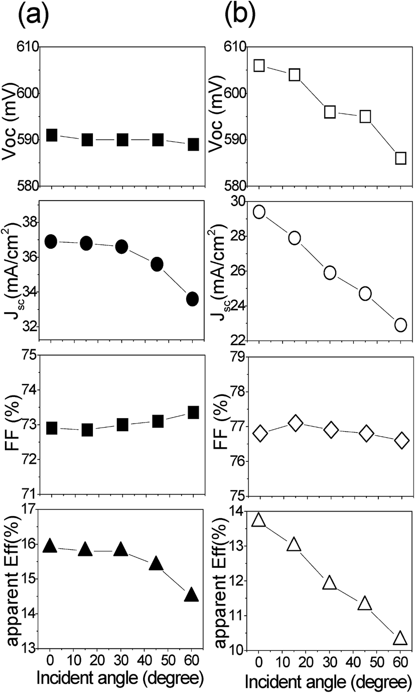 | ||
| Fig. 6 Performances of (a) RJ-HET and (b) P-HET solar cells as a function of incident angle of light. The RJ-HET solar cell shows a much better omnidirectional antireflection property than the P-HET solar cell. | ||
4. Conclusion
In summary, a-Si:H/SiNWs RJ-HET solar cells were fabricated by Cat-CVD combined with MACE. Nice conformal coating of a-Si:H thin film on MACE SiNWs with high aspect ratio and large density was realized. The optimal combination of average length of SiNWs and deposition time of a-Si:H was determined. Optimized thickness (deposition time) of intrinsic a-Si:H layer is 10 nm and doped a-Si:H layer is 20 nm for SiNWs with 1 μm length. The highest efficiency of 16.02% of RJ-HET solar cell was achieved. Capacitance–voltage and dark current–voltage measurements indicate that atomic H treatments and a-Si:H passivation by Cat-CVD reduce the surface recombination effectively and enable a higher Voc for RJ-HET solar cell compared with RJ-HOMO solar cell. Jsc of RJ-HET solar cell increases 24–25% compared with P-HET solar cell due to enhanced light absorption of SiNWs structure and radial collection of carriers. And, the radial collection of carriers has a significant contribution to shortwave response in IQE spectra. RJ-HET solar cell is remarkably insensitive to AOI over a wide range, which indicates an excellent omnidirectional antireflection property.
It should be pointed out that all fabrication processes were carried out in an open lab without air cleaning systems. The interface quality and efficiency of solar cells will certainly be improved if all processes went through in a clean room. In addition, the whole process temperature is below 200 °C, which is suitable for fabrication of ultrathin c-Si solar cell. So, this novel RJ-HET solar cells based on MACE SiNWs and Cat-CVD techniques have great potential in application of high-efficiency and low cost photovoltaic devices in the future.
Conflicts of interest
There are no conflicts to declare.Acknowledgements
This work was supported by the National Natural Science Foundation of China (No. 61674150 and No. 61604153).References
- B. M. Kayes, H. A. Atwater and N. S. Lewis, J. Appl. Phys., 2005, 97, 114302 CrossRef.
- Y. Kuang, M. D. Vece, J. K. Rath, L. V. Dijk and R. E. I. Schropp, Rep. Prog. Phys., 2013, 76, 106502 CrossRef PubMed.
- B. Tian, X. Zheng, T. J. Kempa, Y. Fang, N. Yu, G. Yu, J. Huang and C. M. Lieber, Nature, 2007, 449, 885–889 CrossRef CAS PubMed.
- H. P. Yoon, Y. A. Yuwen, C. E. Kendrick, G. D. Barber, N. J. Podraza, J. M. Redwing, T. E. Mallouk, C. R. Wronski and T. S. Mayer, Appl. Phys. Lett., 2010, 96, 213503 CrossRef.
- B. Dou, R. Jia, H. Li, C. Chen, W. Ding, Y. Meng, Z. Xing, X. Liu and T. Ye, Appl. Phys. Lett., 2012, 101, 183901 CrossRef.
- G. Dong, F. Liu, J. Liu, H. Zhang and M. Zhu, Nanoscale Res. Lett., 2013, 8, 544 CrossRef PubMed.
- J. Oh, H. C. Yuan and H. M. Branz, Nat. Nanotechnol., 2012, 7, 743–748 CrossRef CAS PubMed.
- X. Lin, X. Hua, Z. Huang and W. Shen, Nanotechnology, 2013, 24, 235402 CrossRef CAS PubMed.
- M. A. Green, K. Emery, Y. Hishikawa, W. Warta and E. D. Dunlop, Prog. Photovoltaics, 2017, 25, 3–13 Search PubMed.
- K. Yoshikawa, H. Kawasaki, W. Yoshida, T. Irie, K. Konishi, K. Nakano, T. Uto, D. Adachi, M. Kanematsu and H. Uzu, Nat. Energy, 2017, 2, 17032 CrossRef CAS.
- G. Jia, M. Steglich, I. Sill and F. Falk, Sol. Energy Mater. Sol. Cells, 2012, 96, 226–230 CrossRef CAS.
- K. Li, X. Wang, P. Lu, J. Ding and N. Yuan, Nanoscale Res. Lett., 2013, 8, 396 CrossRef PubMed.
- E. S. Ashour, M. Y. B. Sulaiman, M. H. Ruslan and K. Sopian, Nanoscale Res. Lett., 2013, 8, 466 CrossRef PubMed.
- F. Wang, Y. Jiang, T. Li, Y. Zhao and X. Zhang, J. Mater. Chem. A, 2015, 3, 22902–22907 CAS.
- H.-P. Wang, T.-Y. Lin, M.-L. Tsai, W.-C. Tu, M.-Y. Huang, C.-W. Liu, Yu-L. Chueh and Jr-H. He, ACS Nano, 2014, 8(3), 2959–2969 CrossRef CAS PubMed.
- R. E. I. Schropp, Thin Solid Films, 2015, 595, 272–283 CrossRef CAS.
- R. E. I. Schropp, Thin Solid Films, 2009, 517, 3415–3419 CrossRef CAS.
- S. Osono, Y. Uchiyama, M. Kitazoe, K. Saito, M. Hayama, A. Masuda, A. Izumi and H. Matsumura, Thin Solid Films, 2003, 430, 165–169 CrossRef CAS.
- Q. Wang, S. Ward, L. Gedvilas, B. Keyes, E. Sanchez and S. Wang, Appl. Phys. Lett., 2004, 84, 338–340 CrossRef CAS.
- H. Matsumura, M. Miyamoto, K. Koyama and K. Ohdaira, Sol. Energy Mater. Sol. Cells, 2011, 95, 797–799 CrossRef CAS.
- Q. Wang, M. R. Page, E. Iwaniczko, Y. Xu, L. Roybal, R. Bauer, B. To, H.-C. Yuan, A. Duda, F. Hasoon, Y. F. Yan, D. Levi, D. Meier, H. M. Branz and T. H. Wang, Appl. Phys. Lett., 2010, 96, 013507 CrossRef.
- A. Matsuda, Thin Solid Films, 1999, 337, 1–6 CrossRef CAS.
- C. E. Richardson, Y. B. Park and H. A. Atwater, Phys. Rev. B: Condens. Matter Mater. Phys., 2006, 73, 245328 CrossRef.
- B. Jagannathan, W. A. Anderson and J. Coleman, Sol. Energy Mater. Sol. Cells, 1997, 46, 289–310 CrossRef CAS.
- R. Hussein, D. Borchert, G. Grabosch and W. R. Fahrner, Sol. Energy Mater. Sol. Cells, 2001, 69, 123–129 CrossRef CAS.
- P. Spinelli, M. A. Verschuuren and A. Polman, Nat. Commun., 2012, 3, 692 CrossRef CAS PubMed.
- W. Q. Xie, J. I. Oh and W. Z. Shen, Nanotechnology, 2011, 22, 065704 CrossRef CAS PubMed.
- C. A. Lin, K. Y. Lai, W. C. Lien and J. H. He, Nanoscale, 2012, 4, 6520–6526 RSC.
| This journal is © The Royal Society of Chemistry 2017 |