DOI:
10.1039/C7RA08257F
(Paper)
RSC Adv., 2017,
7, 45185-45194
Synthesis of carbon nanofibers by thermal conversion of the molecular precursor 5,6;11,12-di-o-phenylenetetracene and its application in a chemiresistive gas sensor†
Received
26th July 2017
, Accepted 12th September 2017
First published on 22nd September 2017
Abstract
Carbon nanofibers with an amorphous solid structure have been synthesized by thermal conversion of the polycyclic aromatic hydrocarbon 5,6;11,12-di-o-phenylenetetracene (DOPT) at 1000 °C on various substrates. Rapid annealing of DOPT on copper foil, SiO2/Si wafer and a SiO2/Si wafer coated with a 20 nm thick layer of Pt/Pd resulted in growth of carbon nanofibers. The most effective synthesis of these fibers was realized on the latter substrate. The Pt/Pd layer segregates by dewetting under thermal treatment and forms metallic nanoparticles on which dense networks of amorphous carbon nanofibers were prepared and these were successfully applied in chemiresistor gas sensor applications for detection of toxic gases, e.g. nitrogen dioxide, ammonia and sulfur dioxide. Using an analyte concentration of parts per million, the nanofibers show a very good response towards NO2 and SO2, whereas exposure to ammonia resulted only in negligible, minor changes in the electrical resistance of the sensor.
Introduction
Synthesis of carbon-based nanostructures has tremendously increased over the last two decades. A variety of procedures have been developed and optimized to synthesize carbon nanomaterials of diverse structures, each method having distinct advantages.1–3 In particular, sp2 nanocarbons are in the focus of research with respect to graphene, carbon nanotubes (CNTs) and nanofibers (CNFs).4 The most versatile procedure for the reproducible, scalable synthesis of these carbon nanostructures is the chemical vapor deposition (CVD), in which gaseous carbon precursors are converted on a metal catalyst at elevated temperatures.5–9 The chemical composition of the precursor, the catalyst and the process parameters used, typically define the final structure of the material.10,11 Another interesting approach towards the synthesis of graphene-based nanomaterials which has been demonstrated and might have a broader synthetic scope is the use of solid polycyclic aromatic hydrocarbons (PAHs) like coronene 1, pentacene 2 or rubrene as precursors to carbon nanomaterials (Fig. 1).12–20 PAHs, which can be viewed as small, hydrogen terminated moieties out of a graphitic layer, can be fused together by thermal and/or chemical treatment, yielding layers of graphene like structures,12–16 for example graphene nanoribbons.17–20 In general, reactions leading to such oligomeric structures from PAHs involve C–C coupling reactions which are subsequently followed by cyclodehydrogenation type reactions generating finally the all carbon framework.12,17,18 For example a fusion of coronene 113,16 or of the linear PAH pentacene 212,16 is possible at temperatures as low as 400–800 °C in vacuum. Even the synthesis of highly defective graphene on copper substrates was demonstrated. It was shown that the control of defects by the choice of suitable precursors is possible.15 Moreover, carbon nanotubes have been synthesized using PAHs like xylene and pyrene as precursors in an arc discharge process.21
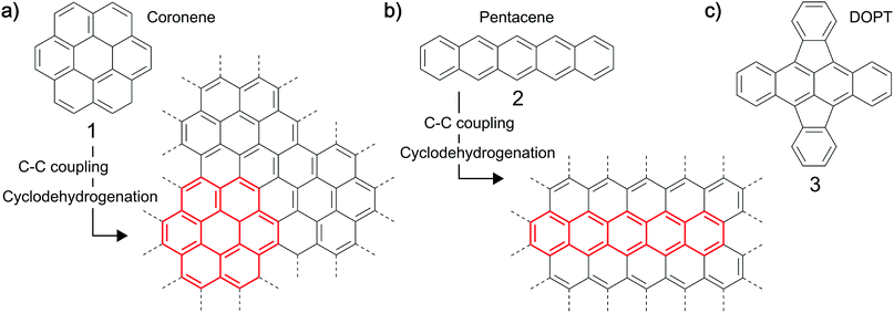 |
| | Fig. 1 Examples for thermal fusion reactions of (a) coronene (1) and (b) pentacene (2) by C–C coupling and cyclodehydrogenation to yield extended graphene-like structures. (c) Structure of the PAH 5,6;11,12-di-o-phenylenetetracene, DOPT, 3 studied herein. | |
Herein, we demonstrate synthesis, characterization and sensoric behaviour of carbon nanofibers with an amorphous structure (a-CNFs) by thermal conversion of the recently available cross conjugated tetracene molecule 5,6;11,12-di-o-phenylenetetracene (DOPT, 3).22,23 The obtained a-CNFs were studied towards their functional properties in a chemiresistor device for the detection of toxic gases. For this, nitrogen dioxide, ammonia and sulfur dioxide were chosen as analyte gases. These are environmentally hazardous and there is need to detect those gases even in smallest concentrations. Our interest in that area stems from the fact that carbon based nanomaterials, e.g. CNTs,24–26 CNFs27–30 and graphene31,32 have proven to be effective alternatives to well-established metal oxide based gas sensors. Key features of these materials compared to metal oxides are operating temperatures as low as room temperature and an increased sensitivity and high versatility introduced by the ease of functionalization of these materials.33 Although a functionalized monolayer of graphene is the most promising material for chemisensoric applications allowing a single molecule detection limit,34 integration into a sensor system can be complex and experimentally laborious. Carbon nanofibers may be inferior to graphene and even CNTs comparing their limits of detection, yet high-yielding synthesis and simple integration in sensor setups make CNFs an interesting nanomaterial for the use in chemiresistors.33
Experimental
Materials and preparation of substrates
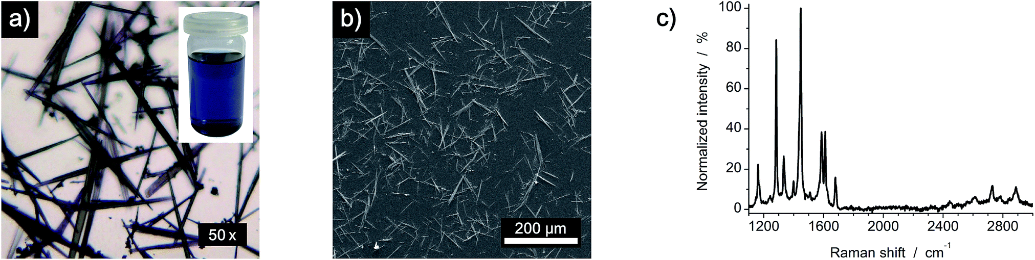
Synthesis of 5,6;11,12-di-o-phenylenetetracene was achieved as reported.22 Saturated solutions of DOPT in dichloromethane (DCM) were prepared by dissolving 2 mg DOPT in 10 mL DCM. Needle-like crystals were deposited on individual substrates by simple drop coating of the as-prepared solution (Fig. 2). As substrates, copper foil (Alfa Aesar, 99.8% purity, 0.025 mm thickness), SiO2/Si wafer (Si-Mat Silicon Materials, thermally grown 600 nm SiO2) and SiO2/Si wafer coated with a 20 nm thick layer of platinum/palladium (Pt/Pd (80/20) disc, 99.99% purity, 0.1 mm thickness), which was deposited by sputter coating (Cressington sputter coater 208HR), were used.
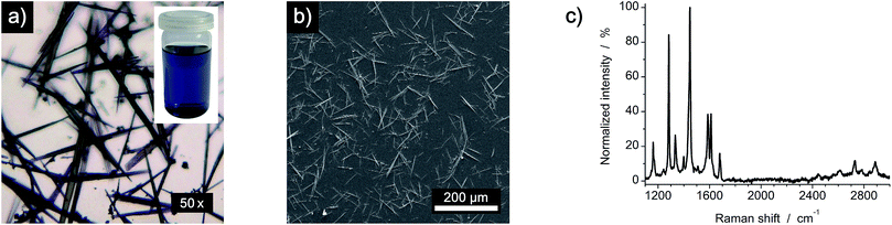 |
| | Fig. 2 Characterization of DOPT before thermal decomposition. (a) Microscopy image of needle-like crystals (inset: solution of DOPT in DCM). (b) SEM image of DOPT after deposition by drop coating. (c) Representative Raman spectrum of DOPT at an excitation wavelength of 514 nm. | |
Thermal transformation of DOPT and synthesis of nanofibers
Thermal transformation was done in a tube furnace (Fa. Horst, Lorsch, 300 mm in length, 30 mm tube diameter), connected to a multi gas controller (MKS Instruments Mass-Flow Controller, MKS Instruments Multi Gas Controller 647 C), pressure controller (Ilmvac VCZ 324) and vacuum pump. The quartz tube extends the length of the tube furnace. A magnetic holder is used to transfer the sample into the hot zone under reduced pressure and to remove them from the furnace immediately after treatment. Samples were placed in the magnetic holder and positioned in the quartz tube outside the hot zone. The setup is evacuated and the furnace is heated to 1000 °C (1 h). Hydrogen (Air Liquide, 99.999 vol% purity) is passed through the system and after a pressure of 10 mbar is reached, the quartz tube is isolated from the set up by closing an inlet and outlet valve. The magnetic holder with samples is instantly placed in the middle of the tube furnace and kept their for either 0.5 h or 5 h. After decomposition, the holder is removed from the hot zone into the cold part of the quartz tube (still under reduced pressure). Samples are cooled to room temperature in vacuum and after a few hours, the system is flushed with argon.
Preparation of chemiresistors and characterization of sensor performance
Chemiresistors are prepared by coating a commercially available sensor substrate (CeramTec) with a 20 nm thick layer of Pt/Pd and DOPT as described before. Sensor substrates are made of alumina with interdigitated Pt electrodes on front side and a Pt heater on the back side (see Fig. S1 in ESI†). Thermal decomposition of DOPT was done for 5 h using identical parameters as before. Gas sensor measurements are performed in a computer-controlled setup equipped with mass-flow controllers (MKS Instruments Mass-Flow Controller, MKS Instruments Multi Gas Controller 647 B), pyrometer (LumaSense Technologies IMPAC IN 5 plus-PL), power supply for temperature regulation (Voltcraft DPS 8003PFC) and a data acquisition/data logger switch unit (Agilent 34972A LXI) for logging electrical resistance of the sensor. A detailed scheme of the experimental setup is given in ref. 35. Pre-mixed gas mixtures of nitrogen dioxide (0.1 vol%), ammonia (0.01 vol%) and sulfur dioxide (0.1 vol%) in nitrogen (Air Liquide, 99.999 vol% purity) were additionally diluted with nitrogen (99.999 vol% purity) and introduced into the glass reactor with the chemiresistor in defined concentration. Analyzed temperatures are 30 °C and 200 °C. The sensors response is given as ΔR/R0 (in %), were R0 is the initial resistance in pure nitrogen and ΔR = Rt − R0 is the change in resistance at a given time t in relation to R0.
Materials characterization
Characterization by optical microscopy was carried out using Olympus CX40 at magnifications of 10× and 50×. SEM (FEI, Philips XL30 FEG) was operated at an acceleration voltage of 30 kV. Micro-Raman spectroscopy (Horiba, LabRAM HR8000, Lab Spec 5) was carried out at a wavelength of 514.5 nm and a magnification of 50×. Amorphous CNFs synthesized on copper foil were additionally transferred onto SiO2/Si by chemical etching for Raman analysis. For TEM characterization, a-CNFs were directly synthesized on a TEM support (Electron Microscopy Sciences) of either copper, SiOx or a grid on which 20 nm of sputtered Pt/Pd had been deposited. TEM was done at an acceleration voltage of 200 keV (FEI Tecnai G2F20@200 keV equipped with EDAX/EDS detector). Additionally, a-CNFs were transferred onto grids coated with lacey carbon film (Electron Microscopy Sciences, lacey carbon film on 300 mesh copper grid) by sonication of a TEM support in ethanol and drop coating of the as-prepared dispersion. XPS (ThermoFisher Scientific, K-Alpha XPS-Spectrometer) was performed using monochromatic aluminium Kα radiation with an acceleration voltage of 8 kV.
Results and discussion
5,6;11,12-di-o-phenylenetetracene (DOPT) 1 precipitates from a toluene solution forming air and light stable needle-like crystals with a length of up to 100 μm. These were deposited on various substrates by drop coating using saturated solutions of DOPT in dichloromethane (Fig. 2). The as-prepared samples were rapidly heated to 1000 °C (<1 min) inside a closed quartz tube under reduced pressure of 10 mbar in a hydrogen atmosphere. Finally, the reaction was terminated by removing the substrate from the hot zone of the furnace either after 0.5 h or 5 h reaction time. Morphological and spectroscopic analysis of the thermal transformation was done using optical microscopy (OM), scanning electron microscopy (SEM), transmission electron microscopy (TEM), micro-Raman spectroscopy (Raman) and X-ray photoelectron spectroscopy (XPS). To study the influence of the substrate on the conversion of DOPT into larger graphitic aggregates, three different substrates were investigated; copper foil, bare silicon dioxide/silicon wafer and a 20 nm thick layer of platinum/palladium (ratio of 80/20) deposited on a SiO2/Si wafer by sputtering.
Conversion reaction of DOPT on copper foil
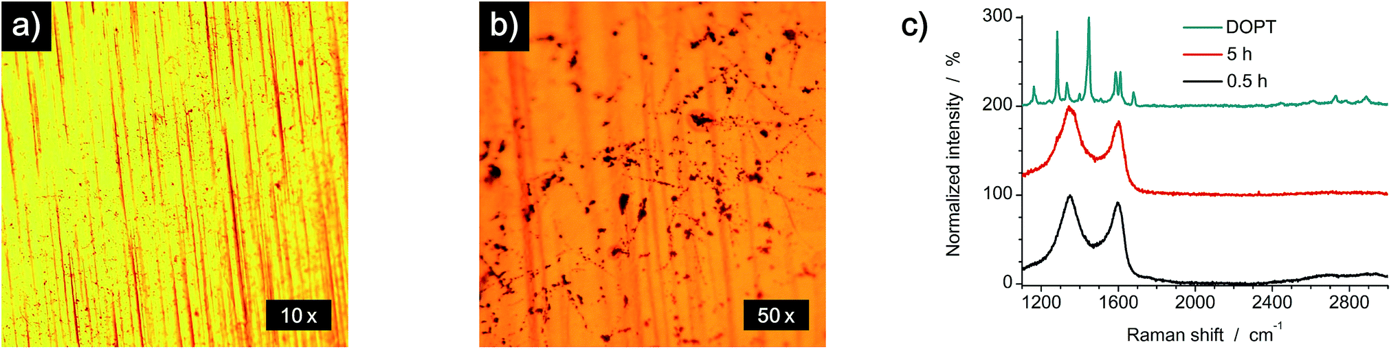
First, we analyzed the thermal decomposition of DOPT on copper foil used for the CVD synthesis of graphene using methane.36 In addition, parameters for the thermal decomposition of DOPT were chosen close to the established CVD process for the synthesis of CVD derived graphene. Thus, thermally induced fusion of the PAH 5,6;11,12-di-o-phenylenetetracene might yield graphene albeit in highly defective composition. Characterization of the annealed samples by optical microscopy confirmed indeed degradation of the needle-like crystals, leaving black coloured residues in similar morphology as the original DOPT crystals behind (Fig. 3a and b). Raman spectroscopy verifies the complete decomposition of DOPT. The D and G peak, which are characteristic for carbon nanomaterials,4 are present in the Raman spectra of these solid black residues (Fig. 3c). The intensity ratio D/G might be indicative for a successful synthesis of carbon nanotubes, nanofibers,37,38 or highly defective graphene.39 Micro-Raman analysis revealed that no carbonaceous material was present in the areas in between the dark material formed.
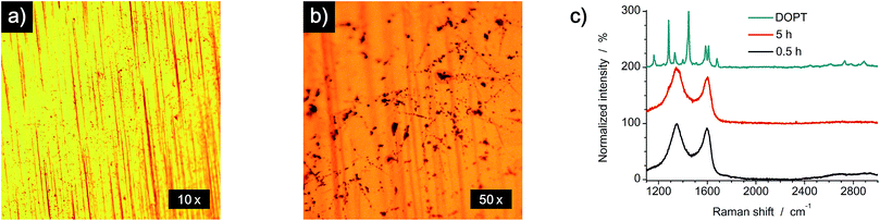 |
| | Fig. 3 Characterization of the copper substrate after thermal decomposition of DOPT at 1000 °C. (a and b) OM images at different magnifications. (c) Raman spectra of DOPT (cyan) and of black residues after thermal annealing at 1000 °C for 0.5 h (black) and 5 h (red). | |
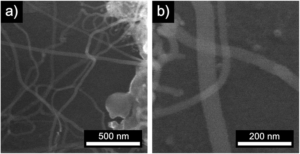
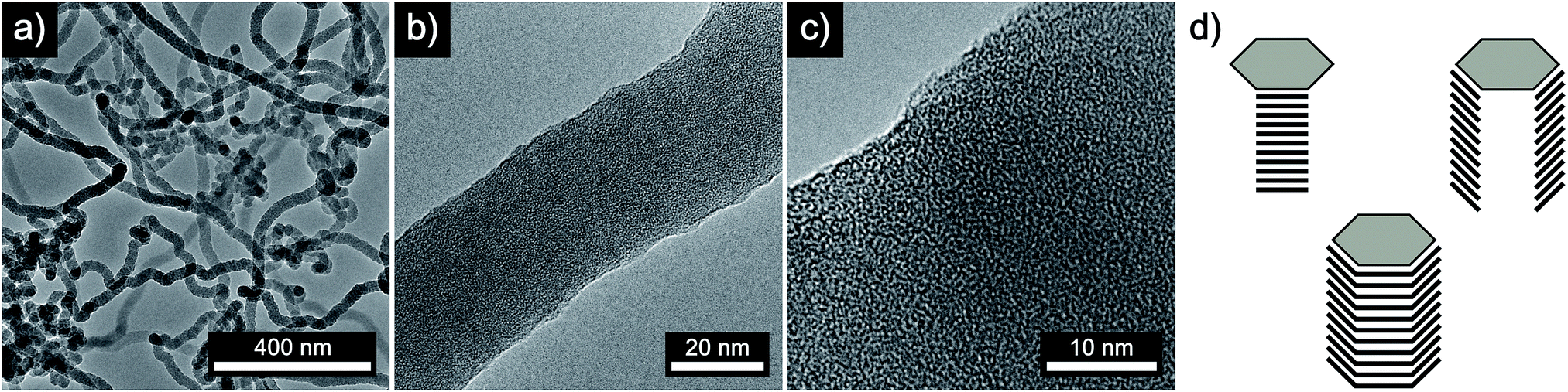
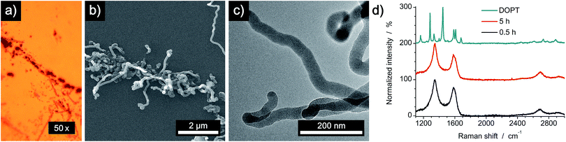
SEM images of the residues directly on the copper substrate after the thermal reaction of DOPT prove the synthesis of one-dimensional nanostructures, which had grown in the positions, where crystals of the intact DOPT molecule were located (Fig. 4). To rule out the formation of graphene in the areas between the dark residues, the copper substrate was etched followed by a transfer process of hypothetically synthesized graphene onto a SiO2/Si wafer. However, no characteristic and indicative Raman peaks of graphene could be detected on the wafer. To finally distinguish carbon nanotubes from carbon nanofibers, DOPT was directly annealed on a copper TEM grid under identical conditions as before. The obtained one-dimensional nanostructures show a highly flexible, solid structure and no sign of metallic incorporations (Fig. 5a and b). For further characterization the CNFs were transferred onto a lacey carbon coated TEM grid employing a short sonication procedure in ethanol followed by drop coating of the dispersion onto a TEM grid. TEM analysis revealed a completely amorphous structure of the CNFs (Fig. 5c). No regular platelet, cup-stacked or herringbone type CNFs were observed (Fig. 5d).40 Even the chosen short sonication time resulted in a destruction of most a-CNFs, also confirming their composition of amorphous carbon. Neither Raman spectra nor SEM microscopic analysis indicated an effect of different annealing times on the structure or morphology of a-CNFs. Mean diameter of the a-CNFs are between 30 nm and 40 nm, yet isolated ones with 70 nm diameter have been detected.
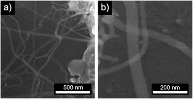 |
| | Fig. 4 SEM characterization of carbon nanostructures formed after thermal annealing of DOPT on copper foil at 1000 °C for 5 h, (a) and (b) show different magnifications. | |
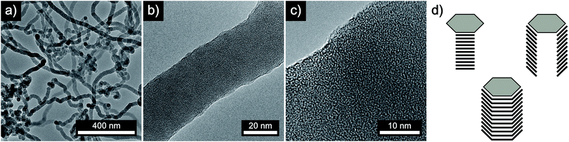 |
| | Fig. 5 Characterization of one-dimensional carbon nanostructures after thermal annealing of DOPT on a copper TEM grid at 1000 °C for 5 h. (a and b) Direct synthesis of a-CNFs on a copper grid and (c) transferred a-CNFs on a lacey carbon coated TEM grid obtained by sonication in ethanol and drop coating. (d) Typical orientation of graphitic layers in crystalline CNFs: platelet, cup-stacked and herringbone type (left to right). | |
Conversion reaction of DOPT on a SiO2/Si wafer
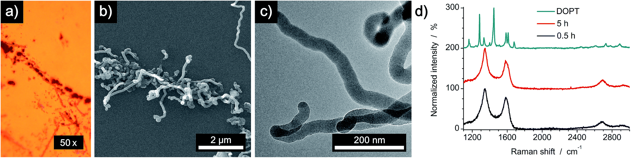
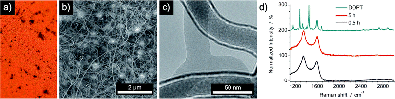
To analyze a possible catalytic effect of the copper substrate on the decomposition of DOPT, similar experiments as before were done using a SiO2/Si wafer as substrate. Analysis by OM, SEM, TEM and Raman spectroscopy confirms synthesis of amorphous carbon nanofibers similar to those formed on the copper substrate (Fig. 6). Black residues on the wafer were visualized by OM (Fig. 6a), whereas SEM images proved the growth of flexible, one-dimensional nanostructures in locations were DOPT crystals had been deposited originally (Fig. 6b). However, there was a significant diameter difference of the a-CNFs observed. The diameter of those increased for longer periods of annealing time from around 30 nm (0.5 h) to 80 nm (5 h). Corresponding SEM images are shown in Fig. S2 in ESI.† Analysis of a-CNFs by TEM, directly synthesized by a thermal reaction from DOPT at 1000 °C on a SiOx-TEM grid in order to mimic the SiO2/Si substrate but to exclude any change caused by transfer etc., shows again flexible a-CNFs similar to the ones observed on the bare copper substrate (Fig. 6c). Raman peaks and ratio of intensities agree as well (Fig. 6d). These results thus indicate no detectable catalytic effect of the previously analyzed copper substrate on the thermal decomposition of DOPT.
 |
| | Fig. 6 Characterization of a-CNFs after thermal annealing of DOPT on a SiO2/Si wafer and on a SiOx-TEM substrate at 1000 °C for 5 h. (a) Optical micrograph image of a-CNFs on a SiO2/Si wafer. (b) SEM image of one-dimensional nanostructures. (c) TEM image of a-CNFs directly synthesized on a SiOx-TEM grid. (d) Raman spectra of DOPT (cyan) and of a-CNFs synthesized on a SiO2/Si wafer after thermal conversion of DOPT at 1000 °C for 0.5 h (black) and 5 h (red). | |
Conversion reaction of DOPT on 20 nm Pt/Pd (80/20) deposited on a SiO2/Si wafer
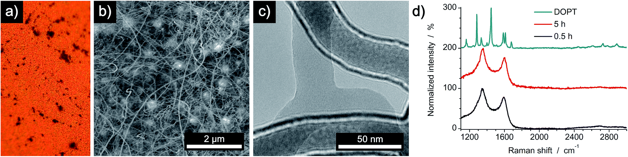
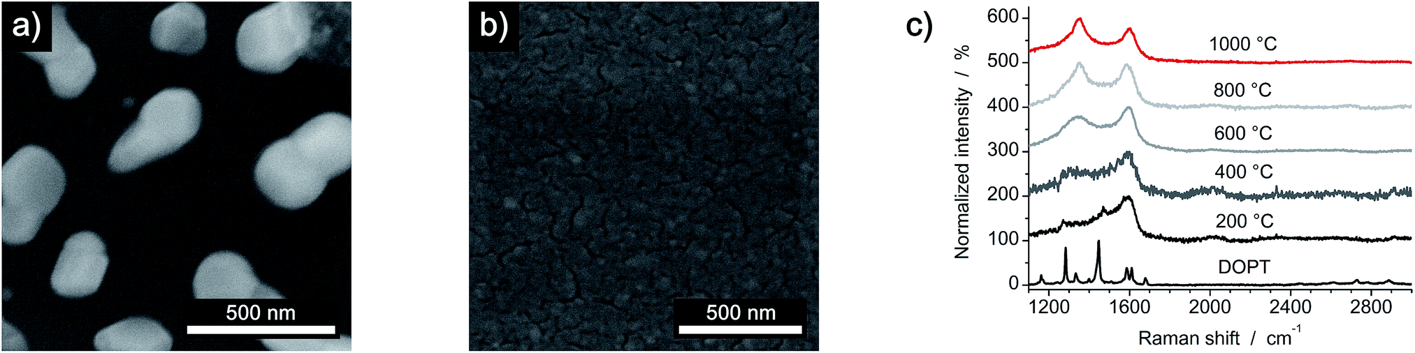
Thermal decomposition of DOPT on a 20 nm thick layer of platinum/palladium (ratio of 80% Pt to 20% Pd), which was deposited on a SiO2/Si wafer (600 nm thermally grown SiO2) by sputter coating was also analyzed. As both noble metals are known to be catalytically active metals in the synthesis of one-dimensional carbon nanomorphologies, an improved synthesis of a-CNFs was expected.41 Analysis by OM indicated a similar thermal decomposition as compared to bare Cu and SiO2/Si substrates as a dark residue was observed after decomposition. However, the colour of the surface changed drastically and it became inhomogeneous during annealing (Fig. 7a). SEM images prove formation of Pt/Pd nanoparticles with an average diameter of 300 nm and also confirm a remarkably increased quantity of as-synthesized a-CNFs as compared to Cu and SiO2/Si substrates (Fig. 7b). Although the number of fibers and/or their length has increased considerably, their average diameter of 30–40 nm is still in the same range as on the former substrates. The increase in synthesis time from 0.5 h (see Fig. S3 in ESI†) to five hours even improved the quantity of a-CNFs. They form a very dense network on the substrate. Analysis by TEM (Fig. 7c) and Raman spectroscopy (Fig. 7d) shows similar results for the grown CNFs.
 |
| | Fig. 7 Characterization of carbon nanofibers after thermal annealing of DOPT on Pt/Pd and SiO2/Si at 1000 °C for 5 h. (a) OM image of residues on the substrate. (b) SEM image of Pt/Pd nanoparticles and network of a-CNFs. (c) TEM image of a-CNFs synthesized on TEM support. (d) Raman spectra of DOPT (cyan) and of a-CNFs after annealing at 1000 °C for 0.5 h (black) and 5 h (red). | |
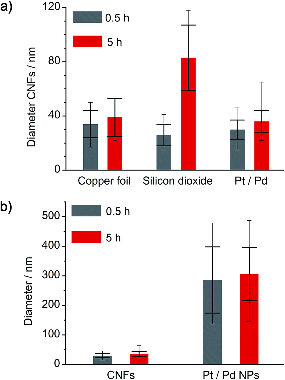
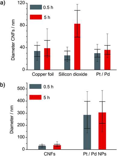
A comparison of the obtained a-CNF diameters on all three substrates is given in Fig. 8a. Whereas most carbon nanofibers have an average diameter of 30–40 nm, synthesis of a-CNFs on SiO2/Si for a total reaction time of 5 h resulted in an increase in diameter to 80 nm. In relation to the size of the Pt/Pd nanoparticles the diameter of the a-CNFs is much lower, indicating the growth of multiple fibers on a single metal particle (Fig. 8b).
 |
| | Fig. 8 Analysis of (a) the diameter variation of a-CNFs, depending on the substrate and the time of annealing at 1000 °C, as well as (b) comparison between a-CNF diameter and size of the Pt/Pd nanoparticles. Larger error bars indicate standard deviation, whereas smaller error bars indicate maximum and minimum numbers of all analyzed diameters. | |
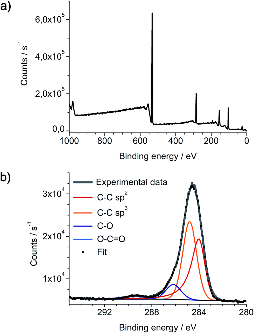
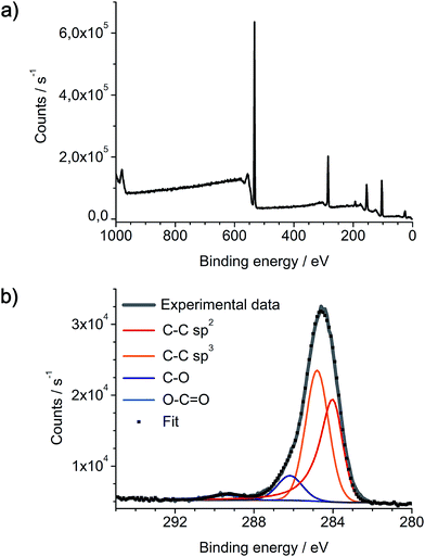
As-prepared networks of carbon nanofibers on Pt/Pd nanoparticles and SiO2/Si substrate were also analyzed by X-ray photoelectron spectroscopy (Fig. 9). XPS spectra reveal the expected presence of carbon, silicon and oxygen, yet platinum and palladium can not be detected. As XPS typically has a penetration depth of only a few nanometers into the surface, these results indicate a complete coverage of the catalyst nanoparticles with a several nanometer thick layer of carbon. This also indicates the initial growth of a-CNFs at the metallic nanoparticles by thermal decomposition of DOPT. The XPS C 1s signal is fitted with four components in the appropriate ratio of 35.4% C–C sp2, 51.7% C–C sp3, 10.7% C–O and 2.2% of O–C![[double bond, length as m-dash]](https://www.rsc.org/images/entities/char_e001.gif) O moieties, respectively. As discrimination of sp2 and sp3 carbon species is difficult, given values are an estimation, yet they are in full agreement with Raman spectra of the a-CNFs. Oxygen based functional groups can either be generated by reaction of a-CNFs with the SiO2 substrate or steaming from oxygen residues residing in the quartz tube walls during gas phase synthesis.
O moieties, respectively. As discrimination of sp2 and sp3 carbon species is difficult, given values are an estimation, yet they are in full agreement with Raman spectra of the a-CNFs. Oxygen based functional groups can either be generated by reaction of a-CNFs with the SiO2 substrate or steaming from oxygen residues residing in the quartz tube walls during gas phase synthesis.
 |
| | Fig. 9 Characterization of a-CNFs by XPS, synthesized by thermal annealing of DOPT on Pt/Pd and SiO2/Si at 1000 °C for 5 h. (a) Survey spectrum and (b) C 1s spectrum of as-prepared a-CNFs on the substrate. Curve fitting was done using a Shirley background and a four component fitting C–C sp2, C–C sp3, C–O and O–CO was employed. | |
We further analyzed the synthesis of carbon nanofibers on thin layers of Pt/Pd at temperatures of 800 °C, 600 °C, 400 °C and 200 °C. Visual analysis by OM (see Fig. S4 in ESI†) and SEM (Fig. 10 and S5 in ESI†) shows no comparable formation of carbon nanostructures at temperatures lower than 1000 °C as it was observed in the other reactions. The formation of nanoparticles from the deposited films is limited to temperatures of 800 °C as minimum. However, a change in Raman spectra of all samples can be detected, indicating that reaction of DOPT may even start at lower temperatures. From 600 °C and higher, defined D and G peak can be distinguished, e.g. growth of a-CNFs may start but is insufficient to be detected neither by SEM nor TEM.
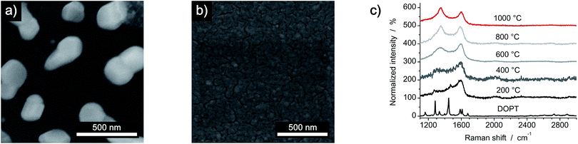 |
| | Fig. 10 Effect of decreasing annealing temperatures on the thermal decomposition of DOPT on Pt/Pd and SiO2/Si. SEM images of samples after annealing at (a) 800 °C and (b) 600 °C for 5 h. (c) Raman spectra of individual samples before (bottom) and after annealing at the given temperatures for 5 h. | |
Study of amorphous carbon nanofibers as chemiresistive gas sensor material
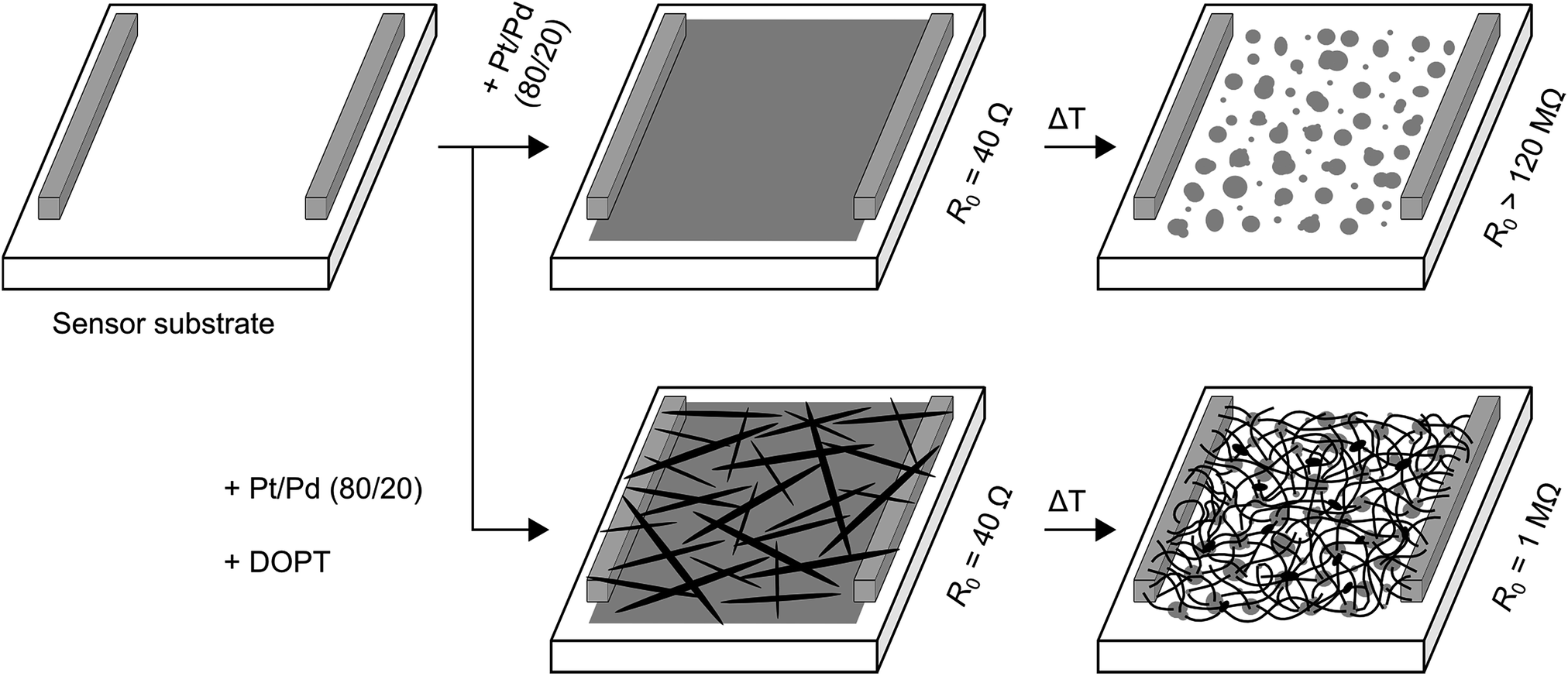
We further analyzed the amorphous carbon nanofibers in a chemiresistive gas sensor for detection of NO2, NH3 and SO2. To avoid transfer and contacting of the one-dimensional nanostructures, we intended to synthesize a-CNFs directly on a sensor substrate. Commercially available sensor substrates are made of alumina with platinum electrodes on the front and a platinum heater on the back side (see Fig. S1 in ESI†). First, a bare layer of platinum/palladium was sputtered on this sensor substrate, resulting in a detectable resistance of about 40 Ω (Fig. 11). After annealing this substrate at 1000 °C without DOPT, formation of nanoparticles occurs on the alumina substrate by dewetting of the as-deposited film. No resistance could be measured (maximum of detectable resistance is 120 MΩ). In another experiment a layer of Pt/Pd and DOPT were deposited on a sensor substrate, yielding Pt/Pd nanoparticles and a dense network of carbon nanofibers after thermal processing at 1000 °C. As the bare layer of Pt/Pd did not show any detectable resistance after annealing, resistance of 1 MΩ refers to the network of a-CNFs. Analysis of the a-CNFs by OM, SEM and Raman (see Fig. S6 in ESI†) confirms similar results compared to decomposition of DOPT on 20 nm Pt/Pd and SiO2/Si substrates as discussed before. In agreement with the amorphous structure of the a-CNFs, their measurable resistance is high and the initial resistance in inert gas atmosphere shows a high noise. Yet, as-prepared networks of fibers can be applied in chemiresistors for the detection of toxic gases. As XPS measurements indicated a complete coverage of the catalyst nanoparticles with a several nanometer thick layer of carbon is observed. An effect of Pt/Pd particles on the sensor performance is therefore not expected. In addition, pure DOPT was analyzed on a bare sensor substrate. As DOPT has a band gap of 2.2 eV,23 no resistance can be detected at room temperature. Also, thermal decomposition of DOPT on the bare sensor substrate did not result in any measurable chemiresistor behaviour, as the short length and low density of the formed a-CNFs prevent contacting of the sensor electrodes.
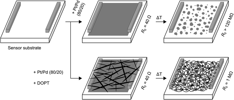 |
| | Fig. 11 Scheme showing formation of a-CNFs on a sensor substrate. First, a sputtered layer of 20 nm Pt/Pd was analyzed. After heating at 1000 °C for 5 h without DOPT, the conducting metallic layer became insulating due to dewetting of the deposited film and formation of isolated Pt/Pd nanoparticles (upper trace). Deposition of DOPT on a layer of Pt/Pd followed by heating the sensor surface to 1000 °C resulted in dewetting and Pt/Pd particle formation and DOPT conversion into a dense network of a-CNFs with a R0 of 1 MΩ (lower trace). R0 is the initial resistance in pure nitrogen and can be detected for values of up to 120 MΩ. For experimental sensor set up see ref. 35. | |
Dynamic response of the as-prepared chemiresistors with R0 = 1 MΩ was analyzed in a nitrogen atmosphere at 30 °C and 200 °C with the gases NO2, NH3 and SO2. Concentration of NO2 and SO2 is in the range of 10–500 ppm, whereas concentration of NH3 is in the range of 10–50 ppm. Instead of plotting the detected real-time resistance Rt, relative change in resistance (Rt − R0) normalized to the initial resistance R0 is shown in Fig. 12. The dense network of a-CNFs shows p-type characteristic, as resistance decreases by exposure to the electron acceptors NO2 and SO2 (e.g. ΔR/R0 < 0%), whereas a slight increase is detected by exposure to the electron donor NH3 (e.g. ΔR/R0 > 0%). Yet, response of the chemiresistor to NH3 is negligible low at all temperatures and hardly exceeds the noise signal of the initial resistance. By comparison, exposure to a similar concentration of NO2 and SO2 results in higher response, yet it decreases with increasing temperature (Fig. 12a and c). Whereas recovery of the a-CNFs is negligible low at room temperature, it clearly improves at 200 °C.
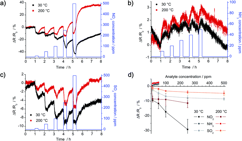 |
| | Fig. 12 Dynamic sensor response and calibration curves of the a-CNF network after exposure to NO2, NH3 and SO2 at 30 °C (black) and 200 °C (red) in nitrogen. Time of exposure to increasing concentration of analyte gas is 20 min, followed by 40 min of purging with pure nitrogen. (a) Exposure to 10, 50, 100, 250 and 500 ppm of NO2. (b) Exposure to 10, 20, 30, 40 and 50 ppm of NH3. (c) Exposure to 10, 50, 100, 250 and 500 ppm of SO2. (d) Correlating calibration curves of the as-prepared chemiresistor. | |
In theory, two possible sensing mechanisms can be expected for the hybrid composite material: (1) gas molecules adsorb onto the Pt/Pd nanoparticles and induce a charge transfer between particles and CNFs. This charge transfer could eventually change the electrical conductivity, e.g. resistance, of the CNF network. Yet, as XPS results indicate a complete coverage of the Pt/Pd nanoparticles with a thick layer of carbon, an influence of Pt/Pd is not to be expected. This first mechanism is therefore negligible. (2) Gas molecules adsorb onto the surface of the CNF network, which provides a continuous pathway for charge carriers between the two electrodes. Depending on the analyte gas, electrons are either transferred from the CNFs to the gas (NO2 and SO2 act as electron acceptors) or from the gas molecules to the CNFs (NH3 acts as electron donor). When exposed to NO2 and SO2, an increasing number of holes in the CNFs results in a decrease in the electrical resistance, e.g. ΔR/R0 < 0%, because CNFs act as p-type transducers.27,28,30 In contrast, exposure to NH3 increases the number of electrons and therefore leads to an increase in electrical resistance. As theoretical calculations prove that the charge transfer from ammonia to carbon nanomaterials is low compared to NO2 and SO2, change in resistance is smaller, confirming the given results.42,43
Lower detection limit (LOD) was calculated by fitting calibration curves (Fig. 12d) with linear and Langmuir isotherms. For a time of exposure of 20 min at 30 °C, calculated LODs are around 4 ppm NO2, 16 ppm NH3 and 4 ppm SO2 respectively. As the change in resistance for lower concentration of analyte gas does not reach a constant value in 20 min, the LODs could even be improved by extending the time of exposure.
Calculated LODs of few parts per million are comparable to chemiresistors fabricated of crystalline carbon nanofibers and are even similar to functionalized fibers decorated with metal nanoparticles.27,28,30,44,45 Yet, one-dimensional single-walled carbon nanotubes detect amounts as low as 125 ppt NO2![[thin space (1/6-em)]](https://www.rsc.org/images/entities/char_2009.gif) 24 and 3 ppb NH3.46 A comparison of sensor data of different carbon materials is given in Table S1 in ESI.†
24 and 3 ppb NH3.46 A comparison of sensor data of different carbon materials is given in Table S1 in ESI.†
To the best of our knowledge, detection of sulfur dioxide using chemiresistors made of carbon nanofibers has not been analyzed yet. Accordingly, given results may act as reference data for future research. Incomplete recovery at room temperature is a general problem for application of carbon nanomaterials in gas sensors and is not limited to carbon nanofibers. Besides increasing the temperature, which simultaneously lowers their sensoric response, irradiation by UV-light also allows fast desorption of analyte molecules.27,44 Main advantage of the as-prepared chemiresistors using a-CNFs is their straightforward and effective method of fabrication. As the a-CNFs are directly synthesized on the substrate connecting the electrodes, any additional treatments, e.g. transfer and/or applying an electrical contact, is unnecessary.
Conclusions
In summary, amorphous carbon nanofibers, a-CNFs, have been synthesized by thermal transformation of the polycyclic aromatic hydrocarbon 5,6;11,12-di-o-phenylenetetracene, DOPT, 3 at 1000 °C. Rapid annealing of DOPT on a copper substrate, on a SiO2/Si substrate or a 20 nm thick layer of Pt/Pd on SiO2/Si yielded highly flexible, amorphous CNFs with an average diameter of 30–40 nm. The quantity of a-CNFs increased drastically when Pt/Pd particles, formed from Pt/Pd thin films by dewetting at temperatures above 800 °C, were used on SiO2/Si substrates compared to metal free substrates. As-synthesized dense networks of amorphous CNFs were applied in chemiresistors for the detection of toxic gases NO2, NH3 and SO2. All fabricated sensors showed good response to low concentration of NO2 and SO2, whereas change in resistance is negligible low for exposure to 10–50 ppm NH3.
Conflicts of interest
There are no conflicts to declare.
Acknowledgements
TEM measurements were performed at the Ernst-Ruska-Zentrum for Elektronenmikroskopie (ER-C), Jülich, Germany, under the cooperative research program ERC-TUD 01. We thank J. Engstler (TUDa) for TEM measurements and L. Houben at ER-C Jülich for technical assistance. XPS measurements were carried out with the support of the Karlsruhe Nano Micro Facility (KNMF), a Helmholtz research infrastructure at KIT, Karlsruhe, Germany. We acknowledge M. Bruns (KIT) for performing XPS measurement and J. Krausmann (TUDa) for measuring Raman spectra.
Notes and references
- Y. Gogotsi and V. Presser, Carbon Nanomaterials, CRC Press, 2nd edn, 2013 Search PubMed.
- W.-W. Liu, S.-P. Chai, A. R. Mohamed and U. Hashim, J. Ind. Eng. Chem., 2014, 20, 1171–1185 CrossRef CAS.
- A. M. Schwenke, S. Hoeppener and U. S. Schubert, Adv. Mater., 2015, 27, 4113–4141 CrossRef CAS PubMed.
- A. Jorio, R. Saito, G. Dresselhaus and M. S. Dresselhaus, in Raman Spectroscopy in Graphene Related Systems, Wiley-VCH Verlag GmbH & Co. KGaA, Weinheim, Germany, 2011, pp. 1–15 Search PubMed.
- X. Chen, L. Zhang and S. Chen, Synth. Met., 2015, 210, 95–108 CrossRef CAS.
- K. A. Shah and B. A. Tali, Mater. Sci. Semicond. Process., 2016, 41, 67–82 CrossRef CAS.
- X. Jiang, Phys. Status Solidi A, 2014, 211, 2679–2687 CrossRef CAS.
- S. Kleckley, H. Wang, I. Oladeji, L. Chow, T. K. Daly, P. R. Buseck, T. Solouki and A. Marshall, in Synthesis and Characterization of Advanced Materials, American Chemical Society, 1997, pp. 51–60 Search PubMed.
- K. Koziol, B. O. Boskovic and N. Yahya, Characterisation and Applications, in Carbon and Oxide Nanostructures - Synthesis, Springer, 2011, pp. 23–49 Search PubMed.
- X. Qi, C. Qin, W. Zhong, C. Au, X. Ye and Y. Du, Materials, 2010, 3, 4142–4174 CrossRef CAS PubMed.
- C. N. He, N. Q. Zhao, C. S. Shi and S. Z. Song, J. Alloys Compd., 2009, 484, 6–11 CrossRef CAS.
- Y. Ishii, T. Sakashita, S. Kawasaki, H. Kato and M. Takatori, Mater. Express, 2011, 1, 36–42 CrossRef CAS.
- A. V. Talyzin, S. M. Luzan, K. Leifer, S. Akhtar, J. Fetzer, F. Cataldo, Y. O. Tsybin, C. W. Tai, A. Dzwilewski and E. Moons, J. Phys. Chem. C, 2011, 115, 13207–13214 CAS.
- X. Wang, L. Zhi, N. Tsao, Ž. Tomović, J. Li and K. Müllen, Angew. Chem., Int. Ed., 2008, 47, 2990–2992 CrossRef CAS PubMed.
- X. Wan, K. Chen, D. Liu, J. Chen, Q. Miao and J. Xu, Chem. Mater., 2012, 24, 3906–3915 CrossRef CAS.
- T. Hayakawa, Y. Ishii and S. Kawasaki, RSC Adv., 2016, 6, 22069–22073 RSC.
- J. Cai, P. Ruffieux, R. Jaafar, M. Bieri, T. Braun, S. Blankenburg, M. Muoth, A. P. Seitsonen, M. Saleh, X. Feng, K. Müllen and R. Fasel, Nature, 2010, 466, 470–473 CrossRef CAS PubMed.
- J. Cai, C. A. Pignedoli, L. Talirz, P. Ruffieux, H. Söde, L. Liang, V. Meunier, R. Berger, R. Li, X. Feng, K. Müllen and R. Fasel, Nat. Nanotechnol., 2014, 9, 896–900 CrossRef CAS PubMed.
- K. A. Simonov, N. A. Vinogradov, A. S. Vinogradov, A. V. Generalov, E. M. Zagrebina, G. I. Svirskiy, A. A. Cafolla, T. Carpy, J. P. Cunniffe, T. Taketsugu, A. Lyalin, N. Mårtensson and A. B. Preobrajenski, ACS Nano, 2015, 9, 8997–9011 CrossRef CAS PubMed.
- D. G. de Oteyza, A. García-Lekue, M. Vilas-Varela, N. Merino-Díez, E. Carbonell-Sanromà, M. Corso, G. Vasseur, C. Rogero, E. Guitián, J. I. Pascual, J. E. Ortega, Y. Wakayama and D. Peña, ACS Nano, 2016, 10, 9000–9008 CrossRef CAS PubMed.
- H. J. Lai, M. C. C. Lin, M. H. Yang and A. K. Li, Mater. Sci. Eng., C, 2001, 16, 23–26 CrossRef.
- T. Wombacher, S. Foro and J. J. Schneider, Eur. J. Org. Chem., 2016, 2016, 569–578 CrossRef CAS.
- T. Wombacher, A. Gassmann, S. Foro, H. von Seggern and J. J. Schneider, Angew. Chem., Int. Ed., 2016, 55, 6041–6046 CrossRef CAS PubMed.
- D. Kumar, P. Chaturvedi, P. Saho, P. Jha, A. Chouksey, M. Lal, J. S. B. S. Rawat, R. P. Tandon and P. K. Chaudhury, Sens. Actuators, B, 2017, 240, 1134–1140 CrossRef CAS.
- A. Goldoni, R. Larciprete, L. Petaccia and S. Lizzit, J. Am. Chem. Soc., 2003, 125, 11329–11333 CrossRef CAS PubMed.
- M. M. Rana, D. S. Ibrahim, M. R. Mohd Asyraf, S. Jarin and A. Tomal, Sens. Rev., 2017, 37, 127–136 CrossRef.
- J. S. Lee, O. S. Kwon, D. H. Shin and J. Jang, J. Mater. Chem. A, 2013, 1, 9099–9106 CAS.
- L. Liao, M. Zheng, Z. Zhang, B. Yan, X. Chang, G. Ji, Z. Shen, T. Wu, J. Cao, J. Zhang, H. Gong, J. Cao and T. Yu, Carbon, 2009, 47, 1841–1845 CrossRef CAS.
- L. Zhang, X. Wang, Y. Zhao, Z. Zhu and H. Fong, Mater. Lett., 2012, 68, 133–136 CrossRef CAS.
- S. Claramunt, O. Monereo, M. Boix, R. Leghrib, J. D. Prades, A. Cornet, P. Merino, C. Merino and A. Cirera, Sens. Actuators, B, 2013, 187, 401–406 CrossRef CAS.
- F. Yavari and N. Koratkar, J. Phys. Chem. Lett., 2012, 3, 1746–1753 CrossRef CAS PubMed.
- W. Yuan and G. Shi, J. Mater. Chem. A, 2013, 1, 10078–10091 CAS.
- E. Llobet, Sens. Actuators, B, 2013, 179, 32–45 CrossRef CAS.
- F. Schedin, A. K. Geim, S. V. Morozov, E. W. Hill, P. Blake, M. I. Katsnelson and K. S. Novoselov, Nat. Mater., 2007, 6, 652–655 CrossRef CAS PubMed.
- J. Patzsch, I. Balog, P. Krauß, C. W. Lehmann and J. J. Schneider, RSC Adv., 2014, 4, 15348 RSC.
- B. Koerbitzer, P. Krauss, C. Nick, S. Yadav, J. J. Schneider and C. Thielemann, 2D Mater., 2016, 3, 24004 CrossRef.
- R. A. DiLeo, B. J. Landi and R. P. Raffaelle, J. Appl. Phys., 2007, 101, 64307 CrossRef.
- Y. Wang, S. Serrano and J. J. Santiago-Avilés, Synth. Met., 2003, 138, 423–427 CrossRef CAS.
- M. S. Dresselhaus, A. Jorio, A. G. Souza Filho and R. Saito, Philos. Trans. R. Soc., A, 2010, 368, 5355–5377 CrossRef CAS PubMed.
- G.-B. Zheng, K. Kouda, H. Sano, Y. Uchiyama, Y.-F. Shi and H.-J. Quan, Carbon, 2004, 42, 635–640 CrossRef CAS.
- S. Esconjauregui, C. M. Whelan and K. Maex, Carbon, 2009, 47, 659–669 CrossRef CAS.
- Y.-H. Zhang, Y.-B. Chen, K.-G. Zhou, C.-H. Liu, J. Zeng, H.-L. Zhang and Y. Peng, Nanotechnology, 2009, 20, 185504 CrossRef PubMed.
- X.-Y. Liu, J.-M. Zhang, K.-W. Xu and V. Ji, Appl. Surf. Sci., 2014, 313, 405–410 CrossRef CAS.
- O. Monereo, S. Claramunt, G. Vescio, H. Lahlou, R. Leghrib, J. D. Prades, A. Cornet and A. Cirera, in 2013 Transducers & Eurosensors XXVII: The 17th International Conference on Solid-State Sensors, Actuators and Microsystems, IEEE, 2013, pp. 1154–1157 Search PubMed.
- J. Jang and J. Bae, Sens. Actuators, B, 2007, 122, 7–13 CrossRef CAS.
- F. Rigoni, S. Tognolini, P. Borghetti, G. Drera, S. Pagliara, A. Goldoni and L. Sangaletti, Analyst, 2013, 138, 7392–7399 RSC.
Footnote |
| † Electronic supplementary information (ESI) available. See DOI: 10.1039/c7ra08257f |
|
| This journal is © The Royal Society of Chemistry 2017 |
Click here to see how this site uses Cookies. View our privacy policy here. 
 Open Access Article
 This Open Access Article is licensed under a Creative Commons Attribution-Non Commercial 3.0 Unported Licence
 and
J. J. Schneider
and
J. J. Schneider