
 Open Access Article
 This Open Access Article is licensed under a
 Creative Commons Attribution 3.0 Unported Licence
An electricity-fluorescence double-checking biosensor based on graphene for detection of binding kinetics of DNA hybridization†
Weiwei Yue abc,
Caiyan Tangabc,
Chunxing Wangabc,
Chengjie Baiabc,
Shuyi Liuabc,
Xiaohui Xieabc,
Hongling Huaabc,
Zhen Zhangabc and
Dengwang Li*abc
abc,
Caiyan Tangabc,
Chunxing Wangabc,
Chengjie Baiabc,
Shuyi Liuabc,
Xiaohui Xieabc,
Hongling Huaabc,
Zhen Zhangabc and
Dengwang Li*abc
aShandong Province Key Laboratory of Medical Physics and Image Processing Technology, School of Physics and Electronics, Shandong Normal University, Jinan 250358, P. R. China. E-mail: dengwang@sdnu.edu.cn
bInstitute of Materials and Clean Energy, Shandong Normal University, Jinan 250358, P. R. China
cSchool of Physics and Electronics, Shandong Normal University, Jinan 250014, P. R. China
First published on 15th September 2017
Abstract
In this paper, the study of an electricity-fluorescence double-checking biosensor and detection system has been presented. The fabrication of the double-checking biosensor was performed by integrating graphene field effect transistors (GFETs) and biosensors based on fluorescence resonance energy transfer (FRET). For the construction of the GFETs as an electrical detection channel, graphene films grown by chemical vapour deposition (CVD) were transferred onto glass substrates. A probe aptamer modified with 6′-carboxy-fluorescein (6′-FAM) was immobilized on the graphene film of the GFETs via 1-pyrenebutanoic acid succinimidyl ester (PBASE) following which graphene oxide (GO) was used to quench the 6′-FAM on the probe aptamer to form the fluorescence detection channel. When the complementary target DNA (tDNA) was introduced into the GFETs, it replaced the GO and was hybridized with the probe aptamer leading to restoration of the fluorescence of the probe aptamer. At the same time, the tDNA hybridized with the probe aptamer leading to the formation of a new double conductive layer of the GFETs, which could change the conductivity of the GFETs. With a home-made double channel detection system, the dynamic hybridization process of the tDNA with the probe aptamer was achieved simultaneously through the electrical and fluorescence channels. Compared with conventional biosensors that are equipped with a single detection mode, this double-checking biosensor could be used to monitor the time and concentration-dependent DNA hybridization kinetics in a reliable and sensitive manner. Furthermore, this work also provides a new strategy for designing biosensors integrated with multiple sensing techniques.
1 Introduction
The detection of binding kinetics of DNA hybridization plays an important role in the diagnosis of diseases,1–5 treatment of pathogen infections3 and forensic tests.4,5 To date, a variety of methods have been studied for the detection of DNA hybridization which mainly include optical6–8 and electrochemical methods.9–11 Among the optical methods, label-free surface plasmon resonance (SPR) is the standard tool for DNA binding detection.12–14 However, because optical responses of SPR sensors depend on the analyte's molecular weight, it is difficult to detect small changes in mass such as oligonucleotide binding. Thus, SPR instrumentation has limitations in terms of sensitivity of quantifying DNA hybridization.15 Moreover, a high-cost dedicated sensor surface along with the integration of optical components is required for SPR, which may increase the overall assay costs and complicate the instrumental setup. Besides SPR, biosensor based on fluorescence resonance energy transfer (FRET) is another optical technology used to monitor DNA hybridization. Due to their special chemical, topological, optical, and electronic properties, nanomaterials have become increasingly important in electronics, catalysis, optics, sensors and other fields. The honeycomb like structure of graphene oxide (GO) facilitates its combination with single stranded DNA through π–π stacking.16,17 The zero-band gap structure of GO makes it an effective fluorescence quencher in FRET sensors. This unique ssDNA–GO interaction has been used in developing biosensors for DNA, proteins, and small molecules by fluorescence method.18–20 P. Alonso-Cristobal et al. reported a DNA sensor based on GO for DNA detection with limit of 5 pM.21 Tapas Paul et al. reported a biosensor to study the hybridization mechanism during noncovalent adsorption and desorption of DNA on graphene oxide.22As for the electrical method, one dimensional nanomaterials such as Si nanowire, carbon nanotube and two dimensional nanomaterials such as topological insulators and graphene are expected to be feasible in biosensor design for real-time detection of a variety of bioactive molecules.23–26 Bunimovich, Y. L. et al. and Duan, X. et al. reported a biosensor based on silicon nanowires for the real-time measurement of DNA hybridization in electrolyte solution25 and quantification of the affinities and kinetics of protein interactions.26 However, the high probe density in nanowires sensors reduces the efficiency of DNA hybridization and kinetics.27 Therefore, reliable and cost effective nano devices are not yet available for quantitative measurement of binding kinetics and affinity of DNA hybridization. Graphene has a 2D honeycomb lattice of carbon with a sp2 structure and possesses large surface to volume ratio,28–31 which facilitates the more efficient adsorption of the probe aptamer and improves the sensitivity of the biosensor as compared with the nanowires sensor. Besides, graphene has high electron mobility, which makes graphene more sensitive to foreign molecules or ions. Foreign ions or molecules can change the doping mode of graphene or establish a double conductive layer, which could modulate the conductivity and the Dirac point of graphene field effect transistors (GFETs). Therefore, graphene has emerged as an ideal conducting channel material for FET biosensors for detection various biomolecules.32–34
In order to improve the reliability of detecting DNA hybridization and for a better understanding of the mechanism of its dynamics, we proposed an electricity-fluorescence double-checking biosensor integrated with a GFET sensor and a FRET sensor. Graphene films grown by CVD were transferred onto glass substrates to construct GFETs as the electrical detection channel. The aptamer modified by 6′-FAM was immobilized onto the GFETs via 1-pyrenebutanoic acid succinimidyl ester (PBASE) as a probe chain. GO was combined with the probe aptamer for quenching the 6′-FAM to form the fluorescent channel. Due to the existence of the target DNA (tDNA), the GO was separated from the probe aptamer and the fluorescence of the probe was restored. Meanwhile, the tDNA replaced the GO and hybridized with the probe chains to construct a new double conductive layer causing conductivity changes of the GFETs. A home-made double channel data acquisition system was constructed to record the fluorescence intensity (FI) and conductivity of the GFETs simultaneously. The hybridization kinetics between tDNA and probe aptamer were obtained in real-time by the double-checking biosensor with high reliability. In addition, this electricity-fluorescence double-checking biosensor displays high sensitivity towards DNA detection at a concentration as low as 50 nM.
2 Experimental
2.1 Materials and methods
The glass substrate with two indium tin oxide (ITO) electrodes was designed and purchased from Hua Nan XiangCheng Ltd. (China). Polymethyl methacrylate (PMMA) was purchased from Sigma-Aldrich (Shanghai, China). The probe aptamer and tDNA were purchased from Sangon Biotech Inc. (Shanghai, China). The sequence of the probe aptamer was 5′-FAM-ACC TGG GGG AGT ATT GCG GAG GAA GGT–NH2-3′ and the sequence of the complementary target DNA was 5′-TGG ACC CCC TCA TAA CGC CTC CTT CCA-3'. PBASE and dimethyl sulfoxide (DMSO) were obtained from Sigma-Aldrich (Shanghai, China). Phosphate buffered saline (PBS, P5368-10PAK) with a pH of 7.4 was purchased from Sigma-Aldrich (Shanghai, China).Raman microscopic system (SPEX-1403, SPEX) was used to characterize the quality of graphene as well as verify the functionalization of the GFETs. The emission spectrum of the excitation LED was measured by an optical fiber spectrometer (USB2000, Ocean Optics). The absorption and emission spectra of probe aptamer were scanned by a fluorescence spectrophotometer (LS55, PerkinElmer). A home-made double channel detection system (DCDS) was used to record electrical and fluorescent signals simultaneously.
For the construction of the DCDS, an LED SMB490R (EPITEX, Japan) was used as the light excitation source for the 6′-FAM and a photomultiplier tube (PMT, H9306-04, Hamamatsu Photonics (China) Co., Ltd.) was selected as an optical–electrical converter device. Convergent lens (Zolix, Beijing, China), collamitor (Wenyi, Shanghai, China), dichroic mirror and an optical filter (Samrock, USA) were used to construct the fluorescence optical unit. Ag/AgCl micro-electrode (R0303, AiDaHengSheng, Tianjin, China) was adopted as the gate electrode in GFETs.
2.2 Fabrication of the GFETs
The process of fabricating a GFET has been shown in Fig. 1(a). Graphene films were prepared by the typical CVD method in our lab.35,36 Graphene grown on the surface of copper foil was transferred onto a glass substrate with two indium tin oxide (ITO) electrodes by wetting transfer methods.37–40 The ITO electrodes were taken as the source and drain electrodes of GFETs. A polydimethylsiloxane (PDMS) chamber was attached on the graphene film as a reaction cell. The photograph of the GFETs was shown in Fig. 1(b). The quality of graphene was determined by a confocal Raman microscopic system (SPEX-1403, SPEX).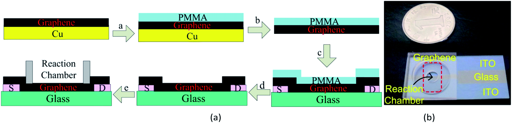 | ||
| Fig. 1 Fabrication of GFETs. (a) Schematic of GFETs fabrication, (b) photograph of a GFET. | ||
2.3 Functionalization of the GFETs
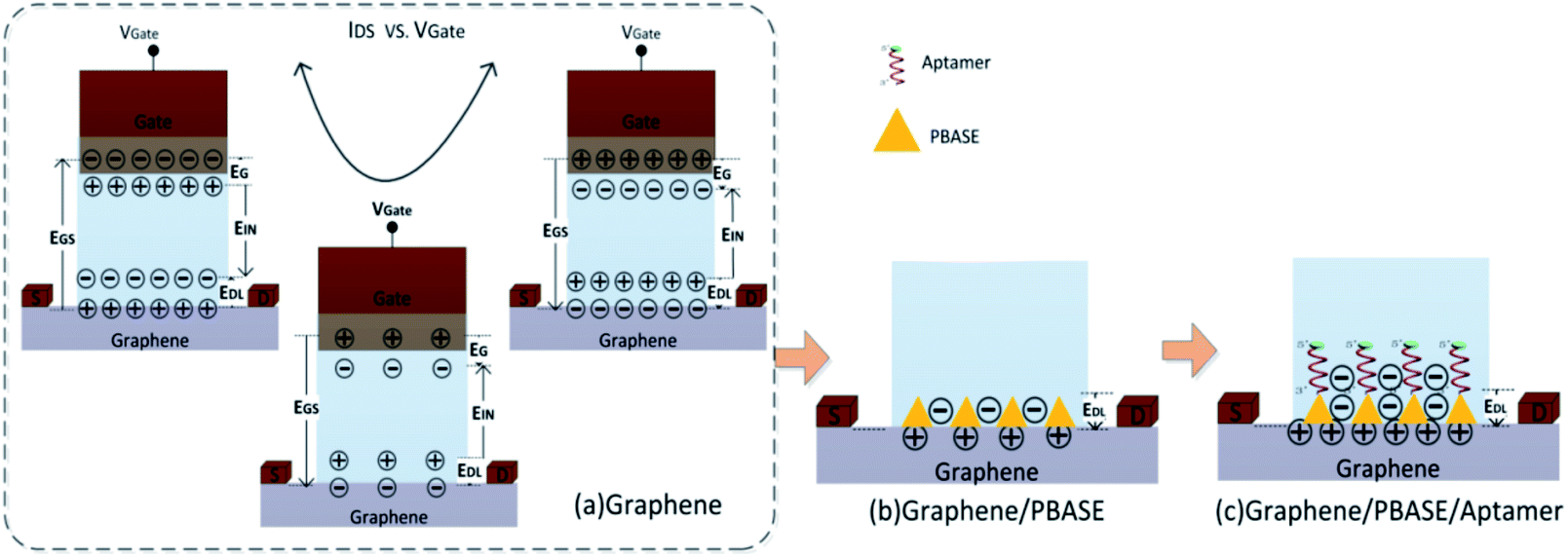
The functionalization process of the GFETs is shown in Fig. 2. Firstly, PBASE with concentration of 10 mM was prepared by dissolved in DMSO as a linker reagent. The prepared PBASE was added into the reaction cell of GFETs for 2 hours at room temperature. Subsequently the reaction cell was washed with DMSO, ethanol and deionized water successively to remove the unmodified PBASE. The PBASE was immobilized on the surface of graphene by π–π stacking between the six-membered ring of the graphene and the pyrene group of PBASE. Secondly, the GFETs immobilized by PBASE were filled with the solution containing 2 μM probe aptamer at room temperature for 4 hours to ensure sufficient reaction time between the probe aptamer and the PBASE. The succinimide portion of the PBASE extends out from the surface of graphene and permits immobilization of probe aptamer through a conjugation reaction between the amine group of the probe aptamer and the succinimide group of PBASE.41–43 The unreacted probe aptamer is removed by 1× PBS solution containing 0.2% SDS, 1× PBS solution and deionized water respectively. Finally, 140 μg ml−1 GO solution was added into the reaction cell for 5 min to quench the fluorescence on the probe aptamer.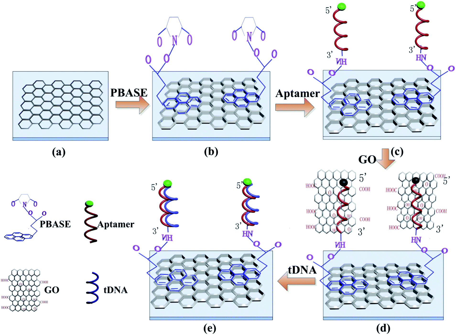 | ||
| Fig. 2 Functionalization and detection principle of the GFETs. (a) Graphene film grown by CVD, (b) functionalization of graphene by PBASE, (c) immobilization of probe aptamer via PBASE, (d) GO to quench the fluorescence of probe aptamer, (e) hybridization of the probe DNA with target DNA. | ||
2.4 Construction of DCDS
A home-made DCDS is shown in the Fig. 3. For the electrical channel, the liquid-gate voltage was generated by a 16 bit D/A module DAC8534 and applied on the GFETs via an Ag/AgCl electrode immersed in the electrolyte. The voltage between source and drain electrode of the GFETs (VDS) was recorded directly through the electric circuit as shown in Fig. 3. The electric current in GFETs (IDS) could be calculated out through the VDS.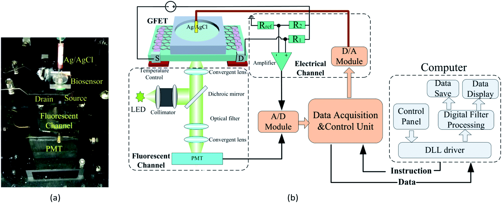 | ||
| Fig. 3 Construction of the double channel detection system. (a) Photograph of the DCDS, (b) schematic of the DCDS. | ||
For constructing the fluorescent channel, the excitation light with a central wavelength of 490 nm was generated from an LED and was converged by a collimator lens into a parallel beam. The beam was then reflected by a dichroic mirror and focused by the converging lens into the reaction cell of GFETs. The emitted fluorescence in the reaction cell passed through a dichroic mirror and was focused by converging lens to the effective area of the PMT. The output of the PMT was recorded to reflect the FI in the reaction cell.
Both the electric voltage and the FI were simultaneously collected and converted into a digital signal via a 16 bit A/D module ADS1256 and then uploaded to a computer via USB.
2.5 Target DNA detection
Detection principle for tDNA is shown in Fig. 2(e). The complementary tDNA was injected into the reaction cell for 1 hour to ensure full incubation between probe aptamer and tDNA. Since the base sequence of tDNA is complementary to that of the aptamer, the affinity of tDNA and aptamer is stronger than that between GO and aptamer, which is based on π–π stacking. The tDNA were hybridized with the probe aptamer to form stable double-stranded structure while GO were released from the probe aptamer strand causing the recovery of the fluorescence of the probe aptamer. Meanwhile, the tDNA replaced the GO and hybridized with the probe aptamer leading to the formation of a new double conductive layer causing conductivity changes of GFETs. Therefore, the FI and IDS of GFETs could reflect the dissociation kinetics of GO from the probe aptamer and hybridization kinetics of tDNA with probe aptamer simultaneously. The DCDS could record the IDS and the FI of the GFETs simultaneously.3 Results and discussion
3.1 Raman characterization
Raman spectroscopy was utilized to characterize the graphene films and to verify the immobilization of PBASE and aptamer respectively on the graphene films as shown in Fig. 4.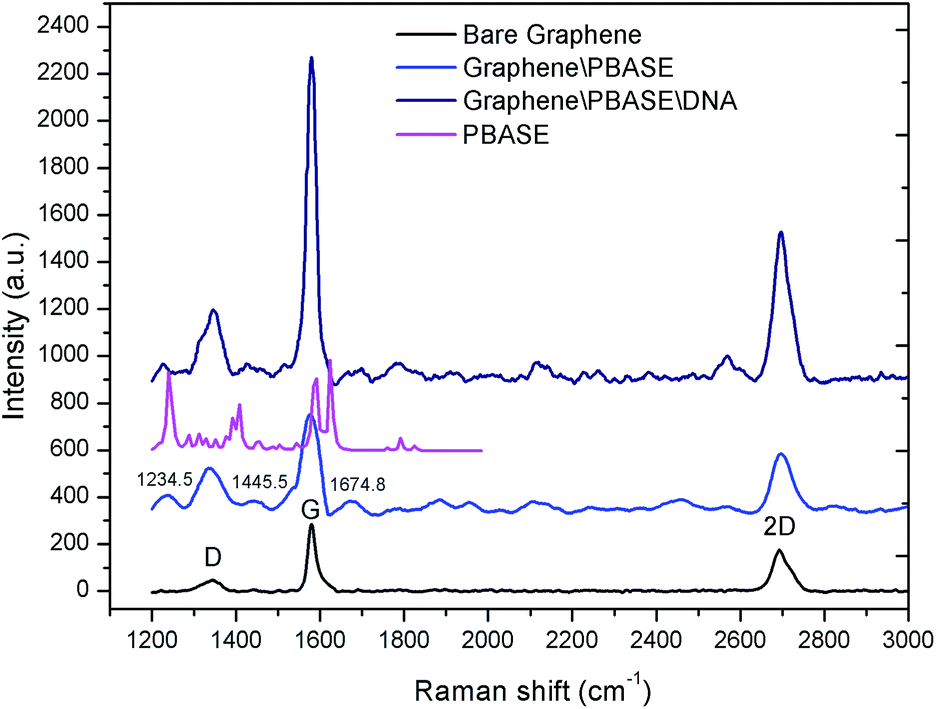 | ||
| Fig. 4 Raman characterization of bare graphene, graphene modified by PBASE and graphene modified by probe DNA. | ||
Raman spectra of the graphene films displayed three bands: D bands at 1360.8 cm−1, G band at 1584.9 cm−1 and the 2D band at 2722.2 cm−1. The 2D band is the characteristic peak of the graphene structure and the strength ratio of the 2D band and G band (I2D/IG) shows that the transferred graphene film is multilayer. After the modification of PBASE on the graphene films, the characteristic peaks of the corresponding molecules were observed in the Raman spectra at 1234.5 cm−1, 1445.5 cm−1 and 1674.8 cm−1. These results are consistent with the Raman spectra of PBASE as shown in Fig. 4. After the modification of graphene with probe DNA, two more peaks are observed in the Raman spectra. The spectral changes of the graphene surface in the Raman spectra demonstrated the successful immobilization of probe aptamer through the PBASE.
3.2 Functionalization of GFETs
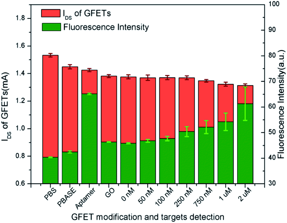
As shown in Fig. 2, the process of modification of GFETs includes the PBASE immobilization on the CVD graphene film as an anchor, probe aptamer interaction with PBASE and GO binding with the aptamer. For each step of the modification process, the DCDS recorded the IDS and the FI simultaneously.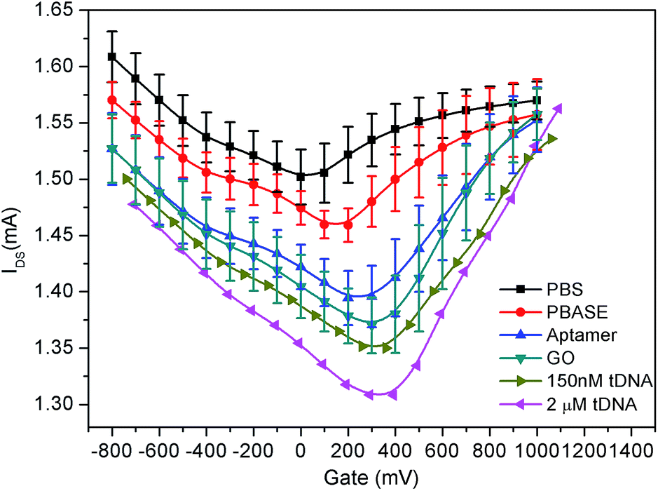 | ||
| Fig. 5 Dirac point voltage of GFETs. | ||
 | ||
| Fig. 6 Schematic of the double conductive layer model. | ||
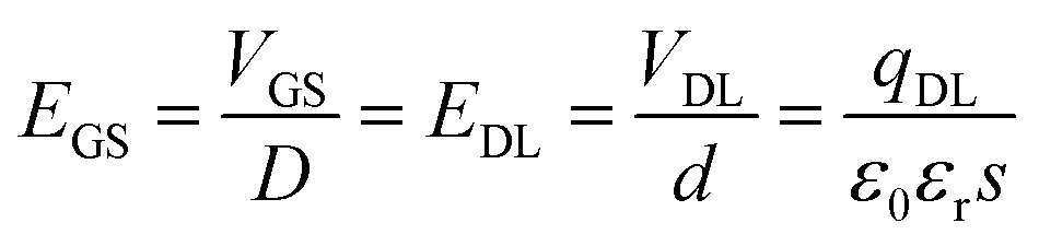
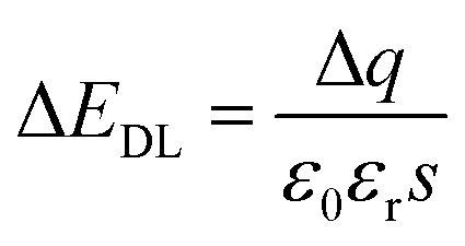
In the GFET's model, the gate electric field (EGS) forms the electric field of a double conductive layer (EDL) on the surface of the graphene through the polar solution electrolyte.44 The capacitance of the double conductive layer could be described by:
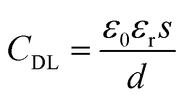 | (1) |
 | (2) |
In the above formula, D is the distance between gate electrode and graphene film. According to the Dirac equation, when the gate voltage (VGS) is 0 V, intrinsic graphene is located at the Dirac point, that is EGS = 0, EDL = 0, qDL = 0.
After the functionalization of graphene, the modified molecules introduce the change of the accumulated charge (Δq) on the double conductive layer capacitor plate.27,44 According to formula (2), the corresponding change in EDL could be represented as:
 | (3) |
In order to make EDL = 0, an external electric field ΔEGS should be applied on the double conductive layer through adding the gate voltage (ΔVGS). That is:
| ΔEGS + ΔEDL = EDL = 0 | (4) |
Therefore, we could obtain the relationship between ΔVGS and the chargeability of the modified molecule as:
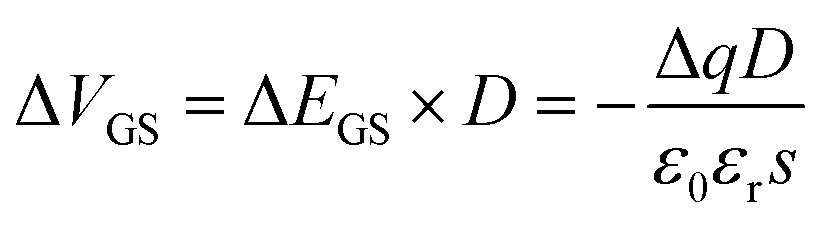 | (5) |
From formula (5) we can conclude that when the modified molecules are negative, ΔVGS is positive indicating that the Dirac point shifts towards the right side and when the modified molecule is positive, the Dirac point shifts towards the left.
As shown in Fig. 5, when the graphene film in the GFET is bare, the Dirac point shift 50 mV to the right (black curve) which was due to the presence of organic residues and trapped air pockets in the wrinkles leading to the p-doping during the preparation of graphene.36,45 After the PBASE immobilization on the surface of the graphene film, as shown in Fig. 5, the Dirac point continued to move towards the right by about 100 mV. The rightward shift of Dirac point is due to the strong electron delocalization of the pyrene group45 and its negative electrons36,45,46 causing p-doping of graphene through the EDL. Since both the probe aptamer strand and GO carry negative charge, the Dirac point continues to shift towards the right corresponding to the fixed state of the probe aptamer and GO on the graphene through the PBASE. Therefore, the results shown in Fig. 5 demonstrate that the shift of Dirac point could reflect the chargeability of molecules on the surface of graphene and also indicate that the probe aptamer has been fixed successfully on the graphene through PBASE.
Meanwhile, with modification of graphene by PBASE, probe aptamer, GO and tDNA successively, it also can be found from Fig. 5 that IDS is gradually reduced which is contradictory to the p-doped enhancement of GFETs. This result can be explained by the fact that the introduction of foreign ions not only brings the doping effect of the GFET, but also widen the energy band-gap of the graphene, which could reduce the conductivity of the graphene.47,48 The IDS of the GFETs in each step of modification was shown in Fig. 7 and its dynamic characteristic in time domain is described in Fig. S1 of the ESI.†
 | ||
| Fig. 7 FI and IDS of GFETs with the modification of PBASE, probe DNA and GO and the combination of tDNA. | ||
Since the excitation and emission light passes through the graphene film, the corresponding absorption spectrum is observed by an ultraviolet spectrophotometer as shown in Fig. S3.† When the wavelength of light is about 520 nm, the transmittance of graphene is more than 90%, which indicates that graphene has little effect on the measurement of FI.
As shown in Fig. 2, GFETs were sequentially modified by PBASE, probe aptamer and GO. After the immobilization of the probe aptamer, the fluorescence was enhanced significantly indicating that it has been modified on the surface of graphene through PBASE as shown in Fig. 7. After adding GO, the FI obviously decreases, which indicated that GO binds with the aptamer and quenched the fluorescence. After combining with different concentrations of tDNA, the fluorescence gradually increased showed that GO was replaced by tDNA leading to fluorescence recovery. The IDS of GFETs was also obtained for each experimental step in Fig. 7.
3.3 Double channel detection of DNA hybridization in time domain
As an application, the electricity-fluorescence double-checking biosensor and detection system was utilized to detect the binding kinetics of DNA hybridization. When the target DNA was added into the GFETs, the tDNA were hybridized with the probe aptamer to form a stable double-stranded structure while GO was released from the probe aptamer strand.32,33,49,50With the gate voltage fixed at 0 mV, the hybridization dynamics curve obtained from the electrical channel is shown in Fig. 8. It can be seen from Fig. 8 that the IDS in the GFET remains almost constant when the tDNA sample was not added to the GFET. When a certain concentration of DNA sample was added into the GFETs, the IDS increased with time which was due to the tDNA substitution GO and hybridization with the probe aptamer to form a new double conductive layer and causing p-doping enhancement. However, for different concentrations of tDNA samples, the IDS of the GFET decreased with increasing tDNA concentration, which was consistent with the results in Fig. 5. This could be explained by the fact that the increase of the foreign negative charges in the electrolyte can increase the graphene band gap, thereby reducing the conductivity of graphene (Fig. S4†).47,48 Therefore, we concluded that the conductivity of the GFETs was determined by the doping effect and the graphene bandgap jointly.
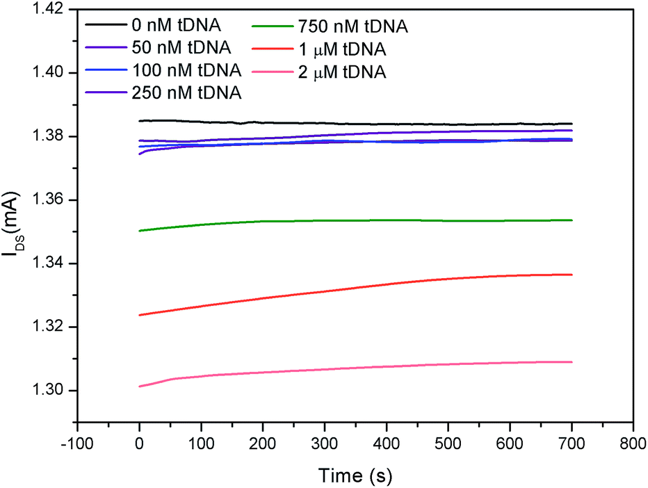 | ||
| Fig. 8 Real-time IDS of the GFETs with different concentrations of tDNA. | ||
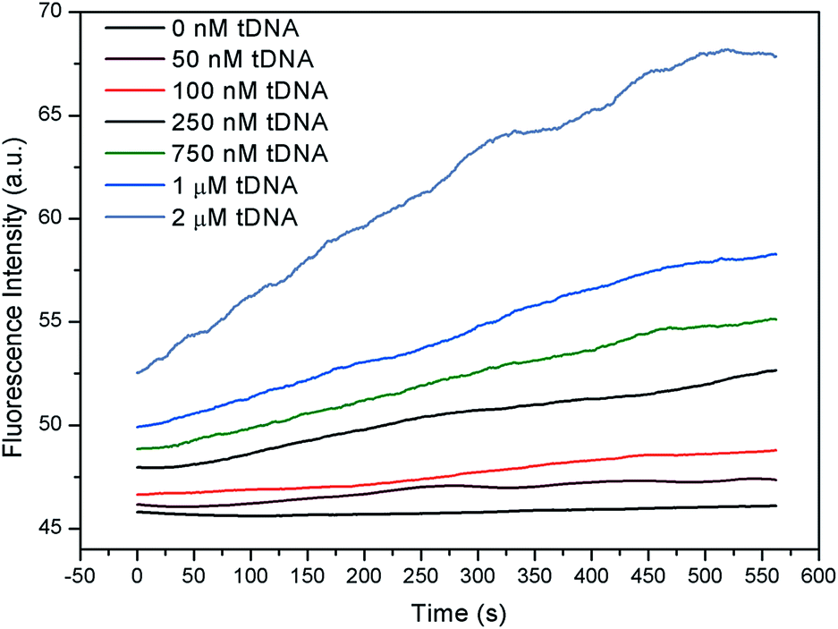
For fluorescent channel, since GO was substituted by tDNA, the fluorescent group on the probe aptamer recovered in the presence of the excitation light as shown in Fig. 9. With the increase in the concentration of the tDNA, the FI and recovery speed were both significantly increased.
 | ||
| Fig. 9 Real-time FI of GFETs with different concentrations of tDNA. | ||
Finally, we observed the hybridization kinetics between tDNA and probe aptamer simultaneously through electrical and fluorescent channels as shown in Fig. 10. We can observe clearly that the FI and IDS of the GFETs change synchronously indicating the dissociation kinetics of GO from probe aptamer and hybridization kinetics of tDNA with probe aptamer simultaneously. With the increase of tDNA concentration, the FI gradually increased and the IDS gradually decreased. Furthermore, the time domain kinetics curves were stable at about 10 minutes, indicating that the hybridization of tDNA to target aptamer was completed.
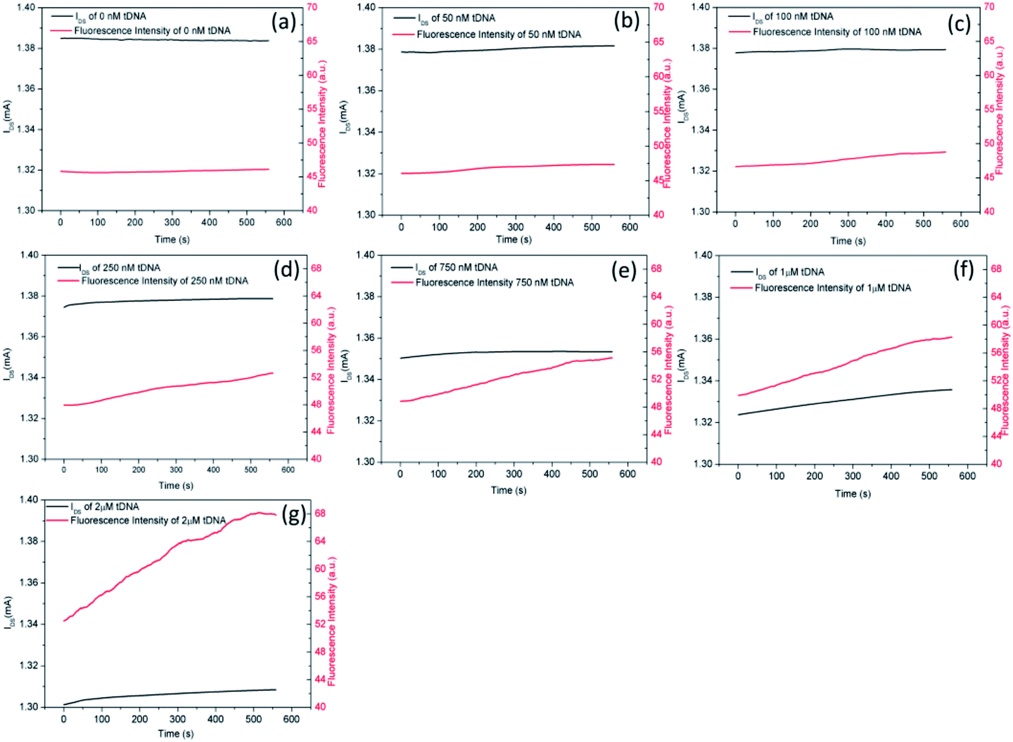 | ||
| Fig. 10 Binding kinetics curves between aptamer and different concentration of tDNA. (a) 0 nM, (b) 50 nM, (c) 100 nM, (d) 250 nM, (e) 750 nM, (f) 1 μM, (g) 2 μM. | ||
3.4 Data fusion of the DCDS
Based on DCDS, we have presented a new data processing method for analysing DNA hybridization kinetics which could contain more information than the conventional technique. Firstly, in order to fuse the IDS and FI of GFETs with same dimension, the DNA kinetics curves depicted in Fig. 10 were normalized through the following formulae:
 | (6) |
 | (7) |
Secondly, we combined IN(T) and FN(T) of tDNA samples with different concentrations, where T was 500 s and corresponding to which, the DNA hybridization process is considered to have been completed. The combined result has been shown in Fig. 11, in which detection channel has been taken as the x axis and the normalized values IN(t = 500 s) and FN(t = 500 s) as the y axis. Since the decrease of IDS and increase of FI, the combined FN(t = 500 s)/IN(t = 500 s) could show a better sensitivity than each single detection channel as depicted in Fig. 12 indicating that the DCDS has better sensitivity than each isolated method. In addition, the synergistic changes of IDS and FI co-detect the tDNA samples, which could also improve the reliability of the results compared with those obtained from single detection method.
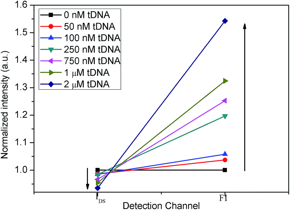 | ||
| Fig. 11 Combination of IN(t = 500 s) and FN(t = 500 s) with different concentrations of tDNA. | ||
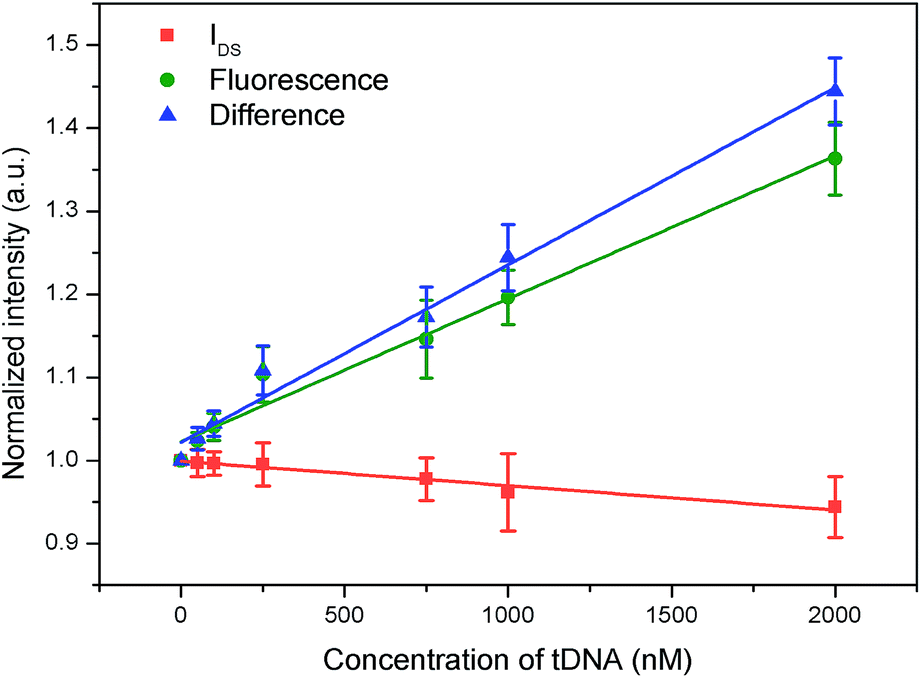 | ||
| Fig. 12 Sensitivity of fluorescence, IDS and combination of DCDS. | ||
Thirdly, we combined IN(t) and FN(t) of each tDNA samples in the entire hybridization process as shown in Fig. 13, in which the detection channel was taken as the x axis and normalized values of IN(t) and FN(t)as the y axis. The following information has been depicted in Fig. 13(a): (1) with the increase of tDNA concentration, fluorescence intensity gradually increased and IDS gradually decreased, (2) the max slope could also reflect the concentration of the tDNA samples, (3) for each tDNA samples, both FI and IDS increased as shown in the enlarged view of Fig. 13(b) and (c), (4) the line gap in the enlarged view Fig. 13(b) and (c) reflected the dynamic hybridization process of tDNA and probe chain and dissociation process of graphene oxide and probe aptamer.
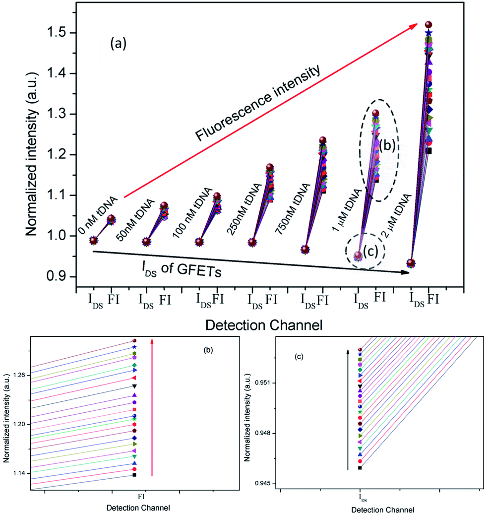 | ||
| Fig. 13 (a) Combination of IN(t) and FN(t) with each tDNA samples in the entire hybridization process. (b) Electrical channel (IDS), (c) fluorescent channel (FI). | ||
4 Conclusions
In summary, we have fabricated an electricity-fluorescence double-checking biosensor and DCDS based on CVD grown graphene. PBASE could be used to immobilize the probe DNA on CVD grown graphene film. GO was used to quench the fluorescence of probe DNA based on the principle of FRET. The double-checking biosensor was used to monitor the binding kinetics of DNA hybridization. The change of FI and IDS simultaneously indicated the dissociation kinetics of GO from the probe aptamer and hybridization kinetics of tDNA with probe aptamer. Compared with the conventional biosensors which use single detection techniques, this method not only enhances the reliability of the testing result, but also is conducive to a better understanding of the mechanism of the dynamics of DNA hybridization. Besides DNA detection, this double-checking sensing method can also be expanded to detect miRNA, RNA and other biomolecules. Furthermore, this work provides a new strategy for biosensor design based on multiple sensing techniques integration.Conflicts of interest
There are no conflicts to declare.Acknowledgements
This research project was jointly supported by the National Natural Science Foundation of China (Grant No. 61401258, 61205174, 61401259 and 11404193).References
- B. J. Cai, S. T. Wang, L. Huang, Y. Ning, Z. Y. Zhang and G. J. Zhang, ACS Nano, 2014, 8, 2632–2638 CrossRef CAS PubMed.
- Q. T. Huang, X. F. Lin, J. J. Zhu and Q. X. Tong, Biosens. Bioelectron., 2017, 94, 507–512 CrossRef CAS PubMed.
- S. S. Liang, L. Qi, R. L. Zhang, M. Jin and Z. Q. Zhang, Sens. Actuators, B, 2017, 244, 585–590 CrossRef CAS.
- S. L. Bai, T. Wang, Z. Zhang, S. C. Sheng, W. Yu and G. M. Xie, Sens. Actuators, B, 2017, 239, 447–454 CrossRef CAS.
- H. T. Ngo, H. N. Wang, A. M. Fales and T. V. Dinh, Anal. Chem., 2013, 85, 6378–6383 CrossRef CAS PubMed.
- M. Tahmasebpour, M. Bahrami and A. Asgari, Optik, 2015, 126, 2747–2751 CrossRef CAS.
- A. S. Ghrera, M. K. Pandey and B. D. Malhotra, Biosens. Bioelectron., 2016, 80, 477–482 CrossRef CAS PubMed.
- M. S. Rahman, M. S. Anower, M. K. Rahman, M. R. Hasan, M. B. Hossain and M. I. Haque, Optik, 2017, 140, 989–997 CrossRef CAS.
- J. Y. Zhuang, L. B. Fu, M. D. Xu, H. H. Yang, G. N. Chen and D. P. Tang, Anal. Chim. Acta, 2013, 783, 17–23 CrossRef CAS PubMed.
- Z. B. Li, X. M. Miao, K. Xing, A. H. Zhu and L. S. Ling, Biosens. Bioelectron., 2015, 74, 687–690 CrossRef CAS PubMed.
- B. C. Zhu, M. A. Booth, P. Shepherd, A. Sheppard and J. Travas-Sejdic, Biosens. Bioelectron., 2015, 64, 74–80 CrossRef CAS PubMed.
- K. Knez, K. P. F. Janssen, D. Spasic, P. Declerck, L. Vanysacker, C. Denis, D. T. Tran and J. Lammertyn, Anal. Chem., 2013, 85, 1734–1742 CrossRef CAS PubMed.
- L. J. A. Macedo, E. N. Miller and A. Opdahl, Anal. Chem., 2017, 89, 1757–1763 CrossRef CAS PubMed.
- O. Zagorodko, J. Spadavecchia, A. Y. Serrano, I. Larroulet, A. Pesquera, A. Zurutuza, R. Boukherroub and S. Szunerits, Anal. Chem., 2014, 86, 11211–11216 CrossRef CAS PubMed.
- P. Teerapanich, M. Pugnière, C. Henriquet, Y. L. Lin, C. F. Chou and T. Leïchlé, Biosens. Bioelectron., 2017, 88, 25–33 CrossRef CAS PubMed.
- Y. Y. Huang, B. Yu, T. Guo and B. O. Guan, RSC Adv., 2017, 7, 13177–13183 RSC.
- C. Li, X. J. Chen, N. Wang and B. L. Zhang, RSC Adv., 2017, 7, 21666–21670 RSC.
- Y. D. Ye, L. Xia, D. D. Xu, X. J. Xing, D. W. Pang and H. W. Tang, Biosens. Bioelectron., 2016, 85, 837–843 CrossRef CAS PubMed.
- Y. H. Liu, L. L. Zhao, J. Zhang, J. Z. Zhang, W. B. Zhao and C. Mao, Talanta, 2016, 161, 87–93 CrossRef CAS PubMed.
- Y. M. Miao, J. Z. Lv and G. Q. Yan, Biosens. Bioelectron., 2017, 94, 263–270 CrossRef CAS PubMed.
- P. Alonso Cristobal, P. Vilela, A. El-Sagheer, E. Lopez Cabarcos, T. Brown, O. L. Muskens, J. Rubio Retama and A. G. Kanaras, ACS Appl. Mater. Interfaces, 2015, 7, 12422–12429 CAS.
- T. Paul, S. C. Bera, N. Agnihotri and P. P. Mishra, J. Phys. Chem. B, 2016, 120, 11628–11636 CrossRef CAS PubMed.
- J. H. Liu, J. Yu, J. R. Chen, R. H. Yang and K. Shih, Mater. Sci. Eng., C, 2014, 38, 206–211 CrossRef CAS PubMed.
- R. Eldawud, A. Wagner, C. Dong, Y. Rojansakul and C. Z. Dinu, Biosens. Bioelectron., 2011, 71, 269–277 CrossRef PubMed.
- Y. L. Bunimovich, Y. S. Shin, W. S. Yeo, M. Amori, G. Kwong and J. R. Heath, J. Am. Chem. Soc., 2011, 128, 16323–16331 CrossRef PubMed.
- X. X. Duan, Y. Li, N. K. Rajan, D. A. Routenberg, Y. Modis and M. A. Reed, Nat. Nanotechnol., 2012, 7, 401–407 CrossRef CAS PubMed.
- S. C. Xu, J. Zhan, B. Y. Man, S. Z. Jiang, W. W. Yue, S. B. Gao, C. G. Guo, H. P. Liu, Z. H. Li, J. H. Wang and Y. Q. Zhou, Nat. Commun., 2017, 8, 14902 CrossRef CAS PubMed.
- C. I. L. Justino, A. R. Gomes, A. C. Freitas, A. C. Duarte and T. A. P. Rocha-Santos, Trends Anal. Chem., 2017, 91, 53–66 CrossRef CAS.
- Y. J. Wu, F. Wang, K. Lu, M. X. Lv and Y. F. Zhao, Sens. Actuators, B, 2017, 244, 1022–1030 CrossRef CAS.
- B. Jin, P. Wang, H. J. Mao, B. Hu, H. L. Zhang, Z. L. Cheng, Z. H. Wu, X. J. Bian, C. P. Jia, F. X. Jing, Q. H. Jin and J. L. Zhao, Biosens. Bioelectron., 2014, 55, 464–469 CrossRef CAS PubMed.
- A. Pandikumar, G. T. S. How, T. P. See, F. S. Omar, S. Jayabal, K. Z. Kamali, N. Yusoff, A. Jamil, R. Ramaraj, S. A. John, H. N. Lim and N. M. Huang, RSC Adv., 2014, 4, 63296–63323 RSC.
- Y. H. Kwak, D. S. Choi, Y. N. Kim, H. Kim, D. H. Yoon, S. S. Ahn, J. W. Yang, W. S. Yang and S. Seo, Biosens. Bioelectron., 2012, 37, 82–87 CrossRef CAS PubMed.
- X. C. Dong, Y. M. Shi, W. Huang, P. Chen and L. J. Li, Adv. Mater., 2010, 22, 1649–1653 CrossRef CAS PubMed.
- Y. X. Huang, X. C. Dong, Y. M. Shi, C. M. Li, L. J. Li and P. Chen, Nanoscale, 2010, 2, 1485–1488 RSC.
- S. C. Xu, B. Y. Man, S. Z. Jiang, J. H. Wang, J. Wei, S. D. Xu, H. P. Liu, S. B. Gao, H. L. Liu, Z. H. Li, H. S. Li and H. W. Qiu, ACS Appl. Mater. Interfaces, 2015, 7, 10977–10987 CAS.
- C. Zhang, B. Y. Man, C. Yang, S. Z. Jiang, M. Liu, C. S. Chen, S. C. Xu, Z. C. Sun, X. G. Gao and X. J. Chen, Nanotechnology, 2013, 24, 395603 CrossRef CAS PubMed.
- Y. Fan, K. He, H. J. Tan, S. Speller and J. H. Warner, Chem. Mater., 2014, 26, 4984–4991 CrossRef CAS.
- M. Lanza, Y. Wang, T. Gao, A. Bayerl, M. Porti, M. Nafria, Y. B. Zhou, G. Y. Jing, Y. F. Zhang, Z. F. Liu, D. P. Yu and H. L. Duan, Nano Res., 2013, 6, 485–495 CrossRef CAS.
- G. H. Zhang, A. G. Güell, P. M. Kirkman, R. A. Lazenby, T. S. Miller and P. R. Unwin, ACS Appl. Mater. Interfaces, 2016, 8, 8008–8016 CAS.
- W. W. Yue, S. Z. Jiang, S. C. Xu, Y. Ma and C. J. Bai, Sens. Actuators, B, 2015, 214, 204–210 CrossRef CAS.
- S. R. Guo, J. Lin, M. Penchev, E. Yengel, M. Ghazinejad, C. S. Ozkan and M. Ozkan, J. Nanosci. Nanotechnol., 2011, 11, 5258–5263 CrossRef CAS PubMed.
- Y. Ohno, S. Okamoto, K. Maehashi and K. Matsumoto, Jpn. J. Appl. Phys., 2013, 52, 110107 CrossRef.
- C. Zheng, L. Huang, H. Zhang, Z. H. Sun, Z. Y. Zhang and G. J. Zhang, ACS Appl. Mater. Interfaces, 2015, 7, 16953–16959 CAS.
- I. Heller, S. Chatoor, J. Männik, M. A. Zevenbergen, C. Dekker and S. G. Lemay, J. Am. Chem. Soc., 2010, 132, 17149–17156 CrossRef CAS PubMed.
- Y. P. Liu, L. Yuan, M. Yang, Y. Zheng, L. J. Li, L. B. Gao, N. Nerngchamnong, C. T. Nai, C. S. S. Sangeeth, Y. P. Feng, C. A. Nijhuis and K. P. Loh, Nat. Commun., 2014, 5, 5461 CrossRef CAS PubMed.
- Y. Q. Wen, F. Y. Li, X. C. Dong, J. Zhang, Q. H. Xiong and P. Chen, Adv. Healthcare Mater., 2012, 2, 271–274 CrossRef PubMed.
- W. J. Zhang, C. T. Lin, K. K. Liu, T. Tite, C. Y. Su, C. H. Chang, Y. H. Lee, C. W. Chu, K. H. Wei, J. L. Kuo and L. J. Li, ACS Nano, 2011, 5, 7517–7524 CrossRef CAS PubMed.
- W. J. Yu, L. Liao, S. H. Chae, Y. H. Lee and X. Duan, Nano Lett., 2011, 11, 4759–4763 CrossRef CAS PubMed.
- Y. Li, L. Sun, J. Qian, L. Long, H. Li, Q. Liu, J. R. Cai and K. Wang, Biosens. Bioelectron., 2017, 92, 26–32 CrossRef CAS PubMed.
- L. Gao, C. Q. Lian, Y. Zhou, L. Yan, Q. Li, C. X. Zhang, L. Chen and K. Chen, Biosens. Bioelectron., 2014, 60, 22–29 CrossRef CAS PubMed.
Footnote |
| † Electronic supplementary information (ESI) available. See DOI: 10.1039/c7ra08246k |
| This journal is © The Royal Society of Chemistry 2017 |