DOI:
10.1039/C7RA08137E
(Paper)
RSC Adv., 2017,
7, 41540-41545
Gas–solid reaction for in situ deposition of Cu3SbS4 on a mesoporous TiO2 film†
Received
24th July 2017
, Accepted 20th August 2017
First published on 25th August 2017
Abstract
Herein, a novel, facile, in situ gas–solid reaction method has been successfully employed for the deposition of famatinite (Cu3SbS4) semiconductor on a mesosporous TiO2 film, where precursors CuCl2 and SbCl3 were first solution-coated on a TiO2 substrate, followed by reaction with H2S gas and further thermal annealing. Various precursor ratios, temperatures and heating atmospheres have been examined for the deposition. The phase-pure Cu3SbS4 has been obtained by coating a mixed solution of CuCl2 and SbCl3 at a molar ratio of 2.5![[thin space (1/6-em)]](https://www.rsc.org/images/entities/char_2009.gif) :1, and annealing at 300 °C for 10 min in an H2S atmosphere. The deposited Cu3SbS4 was uniformly distributed on the entire porous TiO2 film with crystal grain sizes of about 3–4 nm. X-ray photoelectron spectroscopy (XPS) analysis revealed valence states of the synthetic samples for Cu+, Sb5+ and S2−, verifying phase-pure Cu3SbS4. The spectral absorption of the film ranges from 400 nm to 1000 nm with a band gap of ∼1.24 eV. The Cu3SbS4 film shows good and stable photoresponse performance, indicating its high potential as photovoltaic absorber.
:1, and annealing at 300 °C for 10 min in an H2S atmosphere. The deposited Cu3SbS4 was uniformly distributed on the entire porous TiO2 film with crystal grain sizes of about 3–4 nm. X-ray photoelectron spectroscopy (XPS) analysis revealed valence states of the synthetic samples for Cu+, Sb5+ and S2−, verifying phase-pure Cu3SbS4. The spectral absorption of the film ranges from 400 nm to 1000 nm with a band gap of ∼1.24 eV. The Cu3SbS4 film shows good and stable photoresponse performance, indicating its high potential as photovoltaic absorber.
Introduction
Thin film solar cells based on CdTe1 and Cu(In1−xGax)Se (CIGS)2 have drawn much attention due to their excellent absorbance and high efficiencies of nearly 20%. Despite their success, these materials contain toxic (cadmium) and less-abundant elements (tellurium, indium, and gallium). Therefore, cheap, low-toxicity, and earth-abundant metal sulfide semiconductors, such as Cu2ZnSn(S, Se)4 (CZTSSe),3–5 Fe2S,6,7 Cu2FeSnS4 (ref. 8–10) and SnS11,12 have increasingly attracted attention as promising alternatives.
Cu–Sb–S ternary compounds, including four major phases: CuSbS2 (chalcostibite),13–16 Cu12Sb4S13 (tetrahedrite),17,18 Cu3SbS4 (famatinite),19–21 and Cu3SbS3 (skinnerite),22,23 have also emerged as potential absorber materials because of their appropriate optical, electrical properties and the presence of earth-abundant elements.22 Among them, Cu3SbS4 is suggested as a promising light absorber with an optimum band gap energy of ∼1.1 eV, comparable with those of high-efficiency CIGS and CZTSSe materials.24 In the past years, various solution techniques have been explored for the preparation of nano/microscale Cu3SbS4 particles.18,22,24,25 In 2013, J. Embden18 reported the synthesis of Cu12Sb4S13 and Cu3SbS4 nanocrystals through optimizing the ligand chemistry in a hot-injection reaction. Moreover, colloidal nanocrystals of the four different Cu–Sb–S phases were obtained through adjusting the ratios of the precursors and reaction temperatures in the hot-injection method.22 Besides, G. Chen26 studied the synthesis and formation mechanism of flower-like Cu3SbS4 particles via microwave irradiation. In contrast, there were few reports on the in situ preparation of Cu3SbS4 polycrystalline films. Franzer27 reported fabrication of polycrystalline Cu3SbS4 films by magnetron sputtering. Very recently, U. Chalapathi20 reported on the fabrication of Cu3SbS4 thin film by annealing the Sb2S3/CuS stacking layers, where both the Sb2S3 and CuS thin films with appropriate thicknesses are deposited by a chemical bath deposition technique. Both the methods, however, remain inherent disadvantages such as requisite high vacuum or difficulty in the control of the film with desired stoichiometric composition.
Recently, we developed a simple, low-cost, in situ gas–solid reaction method for the deposition of binary metal sulfide Sb2S3, CdS, and ternary CuSbS2.28–30 In this approach, a precursor salt was first introduced from solution into a nanoporous TiO2 film, and subsequently transformed into sulfide through reaction with H2S.28–30 Herein, we further extended this method for the fabrication of Cu3SbS4 film. Through optimizing different precursor concentrations, temperatures and heating atmosphere, pure-phase Cu3SbS4 was achieved. The optical and electrical properties proved that the Cu3SbS4 film could be used as an attractive light absorber in photovoltaics.
Experimental
Fabrication of TiO2/Cu3SbS4 device
First, the soda-lime glasses were cleaned by ultrasonic treatment with detergent, deionized water, ethanol and acetone successively, and then blow-dried by nitrogen gas. 20 nm-sized TiO2 paste (DSL 18NM-T, Dyesol), diluted with ethanol as a mass ratio of 1:1.5, was blade coated on the cleaned glass substrates, followed by calcination at 125 °C for 5 min and 500 °C for 30 min. For the deposition of Cu3SbS4, various ethanolic solutions of CuCl2 and SbCl3 were prepared with the molar ratios of Cu:Sb set as 2:1, 2.3:1, 2.5:1, and 3:1. The precursor solution was first dropped on the mesoporous TiO2 film and kept for 10 s, then spin-coated at 2000 rpm for 20 s. After the coating, the film was rapidly put in an enclosed quartz container full of H2S gas (Fig. 1), which was generated by reaction of 20 wt% sodium sulfide (Na2S·9H2O) and 10 wt% dilute sulfuric acid (H2SO4). With the addition of Na2S solution in the dilute H2SO4, H2S gas was generated and entered into the reaction vessel. The TiO2 film turned dark brown in color upon the addition. After 2 minutes, the film was taken out, washed by ethanol to remove the remnant and resulting by-products, then blown by nitrogen. Afterwards, the film was moved into the quartz container again, and annealed on a hot plate at different temperatures from 200 to 350 °C for 10 min.
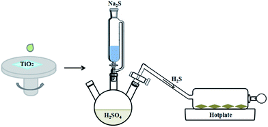 |
| | Fig. 1 Schematic diagram of fabrication procedure for Cu3SbS4 film. | |
Fabrication of Cu3SbS4 device
Fluorine-doped SnO2 (FTO) substrates with a resistivity of ∼10 Ω cm−1 were cleaned with detergent, deionized water, ethanol and acetone successively. On the substrate, a dense titanium dioxide film was prepared as barrier layer to prevent short circuiting through sequentially deposition and annealing of 0.15 M and 0.3 M titanium (diisopropoxide) bis(2,4-pentanedionate) solutions in n-butanol. The TiO2/Cu3SbS4 films were prepared with above-mentioned procedure. Finally, a 60 nm-thick silver (Ag) was deposited on the film as counter electrode by thermal evaporation.
Characterization
Cu3SbS4 thin films were characterized by X-ray diffraction (XRD) using a Bruker D8 Discover diffractometer (with Cu Kα radiation at 1.540598 Å). The surface morphologies and X-ray energy-dispersive spectrometer (EDS) of the Cu3SbS4 thin films were investigated by a field-emission scanning electron microscope (JSM-7500, Japan) and the transmission electron microscopy (TEM) images were acquired with a JEOL HT7700 microscope. X-ray photoelectron spectroscopy (XPS) were performed on the Thermo Scientific ESCA Lab 250Xi using 200 W monochromated Al Kα radiation, and 500 μm X-ray spot was used for XPS analysis. Typically the hydrocarbon C 1s line at 284.8 eV from adventitious carbon is used for energy referencing. The absorption spectra were measured using a UV/Vis/NIR spectrometer (PerkinElmer Lambda 950) and Raman spectrum were recorded on a Bruker Fourier Raman spectrometer (RFS100/S) with a laser excitation wavelength of 532 nm. Ultraviolet photoelectron spectroscopy (UPS) measurement was made on a Specs UVLS using He I excitation (21.15 eV, referenced to the Fermi edge of argon etched gold). The photoresponse performance was conducted on a computer-controlled Keithley 2400 under the illumination of AM 1.5 G. The applied voltage was 20 mV and active area of the device was 0.04 cm−2.
Results and discussion
Preparation for pure-phase Cu3SbS4 film
Fig. 2 shows XRD patterns (a) and Raman spectra (b) of Cu3SbS4 film prepared with molar ratios of Cu:Sb set at 2:1, 2.3:1, 2.5:1, and 3:1, respectively. As shown in Fig. 2(a), the XRD pattern for the 2.5:1 film presents the diffraction peaks at 2θ = 28.70°, 47.78°, 56.66° and 64.75°, corresponding to (112), (204), (312) and (314) faces of famatinite Cu3SbS4 pattern (JCPDS 35-0581).22 All the peaks neither match with those of Sb2S3 or CuS,31,32 nor the peaks of other crystalline structures, such as CuSbS2 (chalcostibite), Cu12Sb4S13 (tetrahedrite) and Cu3SbS3 (skinnerite),24 indicating the complete conversion of CuCl2 and SbCl3 with the ratio at 2.5:1. At lower ratios of 2:1 and 2.3:1, several weak peaks from Sb2S3 can be distinguished, while at the higher ratio of 3:1, the peaks for Sb2S3 disappeared, but new peaks for CuS appeared together with those from Cu3SbS4. Thus, phase-pure Cu3SbS4 could be obtained only at the ratio of around 2.5:1. The deviation from the stoichiometric composition of Cu3SbS4 (3:1) could be explained as follows. In the initial stage of the reaction between the Cu2+/Sb3+ and H2S, CuS and Sb2S3 formed at room temperature, as shown in eqn (1) and (2). During the annealing, the CuS and Sb2S3 reacted to form Cu3SbS4, as shown in eqn (3). In this process, Sb2S3 could gradually volatilize due to its effumability. Therefore, a little excess of Sb3+ precursor is essential to obtain pure Cu3SbS4 phase.| | |
CuCl2 + H2S → CuS + 2HCl↑
| (1) |
| | |
2SbCl3 + 3H2S → Sb2S3 + 6HCl↑
| (2) |
| | |
6CuS + Sb2S3 → 2Cu3SbS4 + S↑
| (3) |
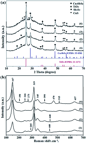 |
| | Fig. 2 XRD patterns (a) and Raman spectra (b) of Cu3SbS4 film prepared by different precursor ratio of 2:1 (1), 2.3:1 (2), 2.5:1 (3) and 3:1 (4) at 300 °C calcination. | |
The Raman spectrum of the 2.5:1 film shows shifts at 147, 198, 246, 273, 319, 345, 398, 515 cm−1 and 637 cm−1. Here, the peaks of 246, 273, 319, 345 cm−1 and 637 cm−1 are close to those of Cu3SbS4 phase,20 while the peaks of 147, 198, 398 cm−1 and 515 cm−1 are from the TiO2 substrate.33 Notably, a distinct peak at 470 cm−1 can be noticed in the spectrum of the 3:1 film, due to the presence of the excess CuS.31 In the case for the 2:1 and 2.3:1 films, a few of weak peaks are observed at 285 and 440 cm−1 from Sb2S3.34 The results are consistent with the phase analysis of XRD. Besides, the elemental composition and EDS spectra of the Cu–Sb–S films are presented in Table 1 and Fig. S1.† It is clear that at the ratio of 2.5:1, the average Cu/Sb/S elemental ratio (2.73:0.92:3.70) is very close to the stoichiometric value of 3:1:4 of Cu3SbS4. All the results indicate that phase-pure Cu3SbS4 film can be synthesized with CuCl2 and SbCl3 at the ratio of 2.5:1 by in situ gas–solid reaction method.
Table 1 Elemental composition of Cu3SbS4 film prepared by different precursor ratio of 2:1, 2.3:1, 2.5:1 and 3:1 (from SEM-EDX)
| Ratio |
2:1 |
2.3:1 |
2.5:1 |
3:1 |
| Cu (%) |
2.97 |
4.12 |
2.73 |
3.27 |
| Sb (%) |
1.15 |
1.43 |
0.92 |
0.95 |
| S (%) |
4.10 |
5.27 |
3.70 |
3.90 |
In previous reports, reaction temperature was regarded as an pivotal factor for controlling the ternary phase composition and crystallinity.5,20 Here, various annealing temperatures ranged from 200 °C to 350 °C were examined, and the corresponding XRD patterns were shown in Fig. 3. The peak intensity for Cu3SbS4 at 2θ = 28.70°, 33.33°, 47.78°, 56.66° and 64.75° are very weak when annealing at 200 °C for 10 min, implying poor crystallinity under this condition.26 Increasing the temperature to 300 °C, the crystallinity is evidently improved with the enhanced intensity of all the peaks. With further increasing the temperature to 350 °C, new peaks for CuS appeared. The observation may imply that at this high temperature annealing, the Cu3SbS4 was partially decomposed to CuS and Sb2S3, and the resulting CuS remained after volatilization of the Sb2S3. Besides, different atmosphere could affect the crystal phases during the annealing (Fig. 4). Here, the annealing was carried out under H2S or N2 atmosphere, respectively. Different from in H2S atmosphere, where only pure Cu3SbS4 phase appeared, both Cu3SbS4 and CuSbS2 phases were observed under N2 annealing ambience. The result implies that H2S environment is requisite to supply adequate amount of S element and avoid the formation of other Cu–Sb–S phases due to the loss of S element during the annealing. All the results demonstrated that pure famatinite Cu3SbS4 film was achieved by the in situ gas–solid reaction with Cu2+:Sb3+ at the ratio of 2.5:1 and annealing in H2S at 300 °C for 10 min. Here, the film prepared with the ratio at 2.5:1 is named as 2.5:1 film for further investigation.
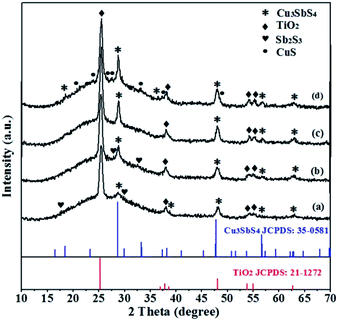 |
| | Fig. 3 XRD patterns of Cu3SbS4 film as a precursor ratio of 2.5:1 heated at different temperatures for 10 min: 200 °C (a), 250 °C (b), 300 °C (c), 350 °C (d). | |
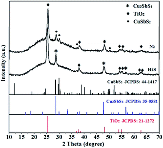 |
| | Fig. 4 XRD patterns of Cu3SbS4 film as a precursor ratio of 2.5:1 heated at H2S and N2 atmosphere at 300 °C for 10 min. | |
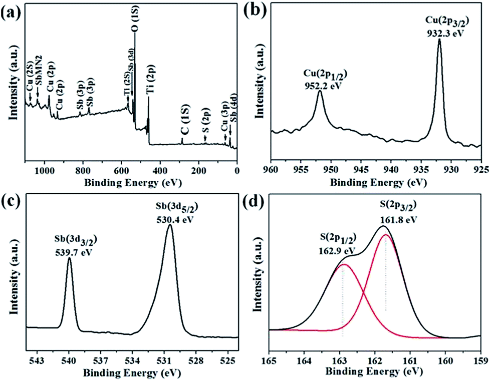
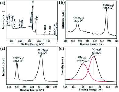
XPS analysis was carried out to investigate the elemental state and composition of the 2.5:1 film. From the full analysis of XPS spectrum (Fig. 5(a)), no peaks were observed for any other elements except Cu, Sb, S, Ti, O and C. Here, carbon element is adventitious used for energy referencing, and the peaks for Ti and O are attributed to porous TiO2 substrate. The spectrum of Cu (Fig. 5(b)) shows two Gaussian peaks at 952.2 and 932.3 eV with a separation of 19.9 eV, which are corresponding to Cu 2p1/2 and Cu 2p3/2 binding state, respectively. The above binding energies are well consistent with reported values for Cu+.35 The antimony presents doublet at the binding energies at 539.7 eV (3d3/2) and 530.4 eV (3d5/2), which are in good agreement with those of Sb5+, and no peaks are observed at 538.7 and 529.2 eV for Sb3+.20,36 The peaks at 162.9 and 161.8 eV represent the S 2p1/2 and 2p3/2, respectively, which are consistent with the chemical state of sulfur (S2−) in the Cu3SbS4. Thus, XPS analysis indicates that the elemental state of the 2.5:1 film are (Cu+)3(Sb5+)(S2−)4.
 |
| | Fig. 5 X-ray photoelectron spectra (XPS) survey scan (a), Cu (2p) (b), Sb (3d) (c), and S (2p) (d) core levels of 2.5:1 film and heat treatment in H2S at 300 °C. | |
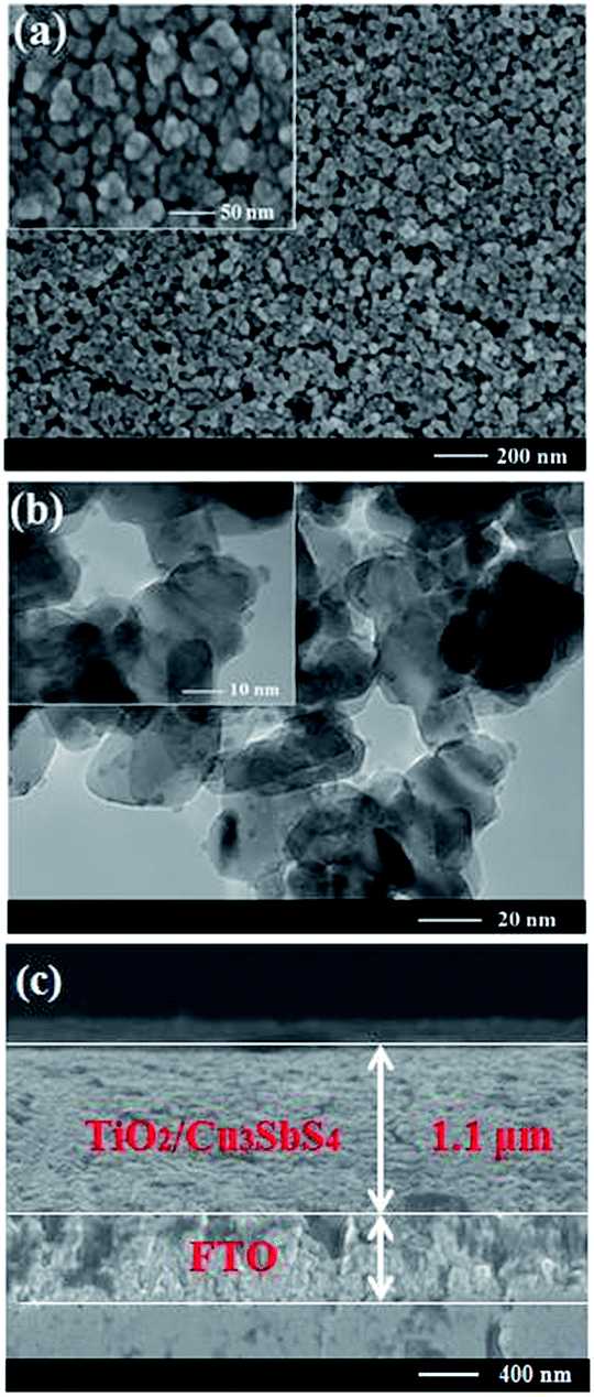
The microstructure of the 2.5:1 film was further evaluated by recording the SEM and TEM images (in Fig. 6). According to the top-view SEM, uniform morphology is evident with many tiny Cu3SbS4 particles homogeneously distributed within the TiO2 film, where the specific particle size could hardly be distinguished. In the TEM, lots of small granules of Cu3SbS4 can be observed on the surface of 20 nm TiO2 balls with crystal grain sizes of about 3–4 nm. Besides, the cross sectional SEM (Fig. 6(c)) displays the thickness of TiO2/Cu3SbS4 is about 1.1 μm. From the cross section, the mapping images were recorded, as shown in Fig. S2,† manifesting the homogeneous deposition of Cu, Sb and S elements in the TiO2 film.
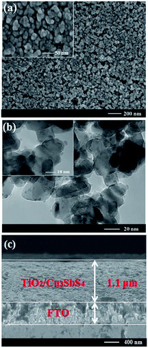 |
| | Fig. 6 Top-view SEM (a), TEM (b) and cross sectional SEM (c) images of Cu3SbS4 film prepared by in situ gas–solid reaction method as a precursor ratio of 2.5:1 film and heat treatment in H2S at 300 °C. | |
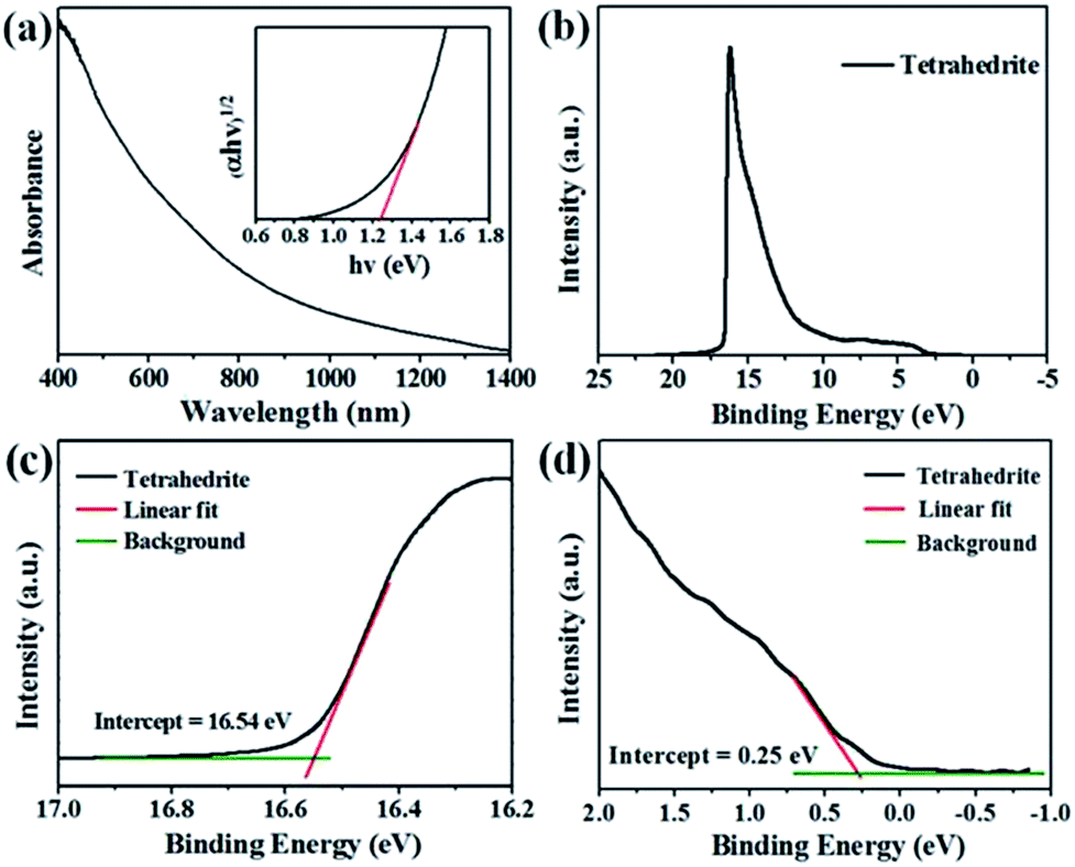
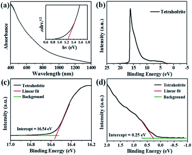
The determination of band gap and positions are significant for a potential photovoltaic absorber material. The UV-Vis-NIR absorption spectrum of Cu3SbS4 film shows a wide absorption range from 400 nm to 1000 nm. The (αhν)1/2 versus hν curves (Tauc plots, inset of Fig. 7(a)) is plotted, and band gap is estimated to be 1.24 eV, which is closed to the reported band gap of 1.2 eV for Cu3SbS4.22,26 Moreover, UPS was applied to determine valance band and Fermi energies of this film. From intercept of 16.54 eV for secondary electron onset and Au energy of 21.15 eV, Fermi energy position relative to vacuum is calculated to be −4.61 eV. The distance between Fermi energy and valance band is 0.25 eV by extrapolating and linear fitting the long tail of UPS spectrum. Combining with the band gap of 1.24 eV estimated from UV-Vis-NIR spectra, the valence band edge and conduction band edge are determined to be located at 4.86 eV and 3.62 eV relative to vacuum, respectively, which suggests its potential application as one kind of solar absorber materials.17,37 The band alignment diagrams of TiO2/Cu3SbS4 film were given as shown in Fig. S3.† It is clear that there exists some excessive driving energy (−0.6 eV) for electron transfer, potentially leading to relatively low theoretical voltage. Thus, it will be desirable to select other N-type electrodes with relatively lower conduction band edge for high open-circuit voltages in the future studies.
 |
| | Fig. 7 UV-Vis-NIR absorption spectra and Tauc plots (a) and UPS full spectrum (b) of 2.5:1 film. Linear fitting of UPS spectrum in the range of 16.2–17.0 eV (c) and −1.0 to 2.0 eV (d). | |
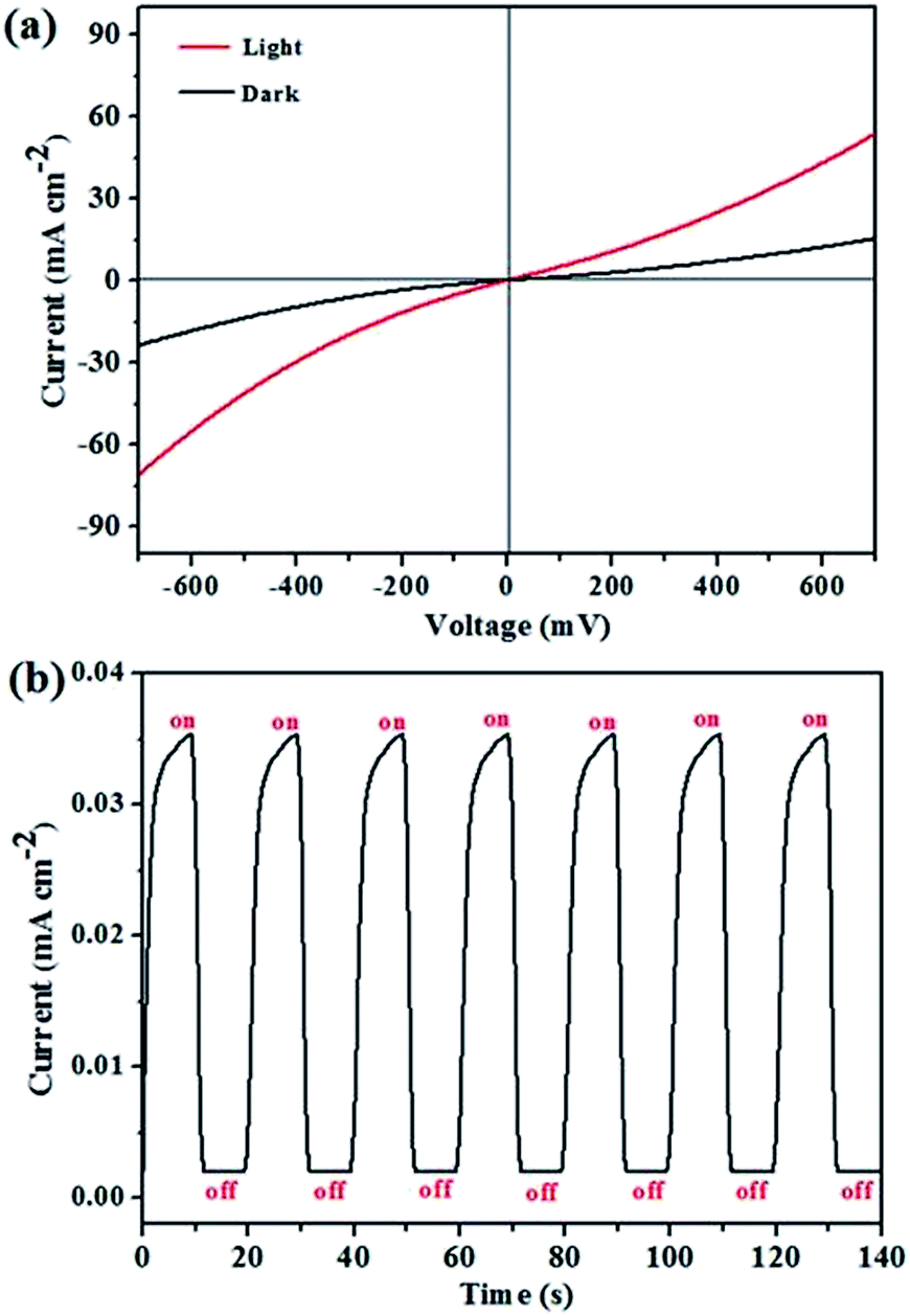
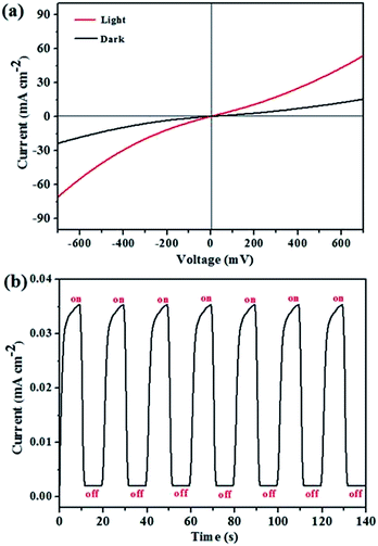
Photoresponse performance was investigated to evaluate the quality of the 2.5:1 film, and the results are presented in Fig. 8. The current–potential (I–V) curves are nearly linear, indicating ohmic contact between silver counter electrode and Cu3SbS4 semiconductor. Compared with dark current, the corresponding photocurrent increased remarkably over the entire bias ranged from −700 mV to 700 mV, which is attributed to excited charge carriers by simulated sunlight, leading to high photocurrent. Besides, photocurrent response curve conducted under a bias of 20 mV presents an excellent photoresponse and high photostability. The dark current of 1.96 × 10⁻³ mA cm−2 dramatically rises to 3.50 × 10⁻² mA cm−2 when the light was on, and the light current drops rapidly as soon as light source was turned off. Despite repeating switch cycle for several times, photocurrent still remains at 3.48 × 10⁻² mA cm−2 without observable attenuation. Above all, Cu3SbS4 made by in situ gas–solid reaction method exhibits high photoresponse performance and provides a possibility to be used as photovoltaic absorption layer.
 |
| | Fig. 8 Current–potential curves (a) and photocurrent response curve (b) under darkness and light for Cu3SbS4 device prepared by in situ gas–solid reaction method. | |
Conclusions
In this report, an in situ gas–solid reaction method has been successfully employed for the deposition of pure-phase Cu3SbS4 film. Various precursor molar ratios, temperatures, and heating atmospheres have been explored for the deposition. The results show that phase-pure Cu3SbS4 can be obtained by the in situ gas–solid reaction with the molar ratio of CuCl2 and SbCl3 at 2.5:1, and annealing in H2S at 300 °C. The Cu3SbS4 particles with crystal grain sizes of about 3–4 nm are uniformly distributed on the porous TiO2 film. The Cu3SbS4 film shows a broad absorption ranged from 400 nm to 1000 nm with the band gap of 1.24 eV. Moreover, the Cu3SbS4 film presents high and stable photoresponse performance, indicating its potential application as solar absorber materials.
Conflicts of interest
There are no conflicts to declare.
Acknowledgements
This work was supported by the 973 Program (No. 2013CB933004), the National Nature Science Foundation of China (Grant No. 61405207, 21174149, 21572235, 51473173, 91433202 and 21221002), and the “Strategic Priority Research Program” of Chinese Academy of Sciences (Grant No. XDA09020000 and XDB12010200). The measurements of (NMR, Mass Spectrometry, XRD, Photoelectron Spectroscopy) were performed at the Center for Physicochemical Analysis and Measurements in ICCAS.
References
- M. Gloeckler, I. Sankin and Z. Zhao, IEEE J. Photovolt., 2013, 3, 1389–1393 CrossRef.
- P. Jackson, D. Hariskos, R. Wuerz, O. Kiowski, A. Bauer, T. M. Friedlmeier and M. Powalla, Phys. Status Solidi RRL, 2015, 9, 28–31 CrossRef CAS.
- S. C. Riha, B. A. Parkinson and A. L. Prieto, J. Am. Chem. Soc., 2009, 131, 12054–12055 CrossRef CAS PubMed.
- H. Katagiri, K. Jimbo, S. Yamada, T. Kamimura, W. S. Maw, T. Fukano, T. Ito and T. Motohiro, Appl. Phys. Express, 2008, 1, 041201 CrossRef.
- A. S. R. Chesman, N. W. Duffy, S. Peacock, L. Waddington, N. A. S. Webster and J. J. Jasieniak, RSC Adv., 2013, 3, 1017–1020 RSC.
- J. Puthussery, S. Seefeld, N. Berry, M. Gibbs and M. Law, J. Am. Chem. Soc., 2011, 133, 716–719 CrossRef CAS PubMed.
- M. Wang, D. Xue, H. Qin, L. Zhang, G. Ling, J. Liu, Y. Fang and L. Meng, Mater. Sci. Eng., B, 2016, 204, 38–44 CrossRef CAS.
- C. Yan, C. Huang, J. Yang, F. Liu, J. Liu, Y. Lai, J. Li and Y. Liu, Chem. Commun., 2012, 48, 2603–2605 RSC.
- X. Jiang, W. Xu, R. Tan, W. Song and J. Chen, Mater. Lett., 2013, 102, 39–42 CrossRef.
- L. Li, X. Liu, J. Huang, M. Cao, S. Chen, Y. Shen and L. Wang, Mater. Chem. Phys., 2012, 133, 688–691 CrossRef CAS.
- P. Sinsermsuksakul, K. Hartman, S. B. Kim, J. Heo, L. Sun, H. H. Park, R. Chakraborty, T. Buonassisi and R. G. Gordon, Appl. Phys. Lett., 2013, 102, 053901 CrossRef.
- K. T. R. Reddy, N. K. Reddy and R. W. Miles, Sol. Energy Mater. Sol. Cells, 2006, 90, 3041–3046 CrossRef.
- S. Suehiro, K. Horita, M. Yuasa, T. Tanaka, K. Fujita, Y. Ishiwata, K. Shimanoe and T. Kida, Inorg. Chem., 2015, 54, 7840–7845 CrossRef CAS PubMed.
- L. Wan, C. Ma, K. Hu, R. Zhou, X. Mao, S. Pan, L. H. Wong and J. Xu, J. Alloys Compd., 2016, 680, 182–190 CrossRef CAS.
- T. Rath, A. J. MacLachlan, M. D. Brown and S. A. Haque, J. Mater. Chem. A, 2015, 3, 24155–24162 CAS.
- Y. C. Choi, E. J. Yeom, T. K. Ahn and S. Seok II, Angew. Chem., Int. Ed., 2015, 54, 4005–4009 CrossRef CAS PubMed.
- L. Wang, B. Yang, Z. Xia, M. Leng, Y. Zhou, D.-J. Xue, J. Zhong, L. Gao, H. Song and J. Tang, Sol. Energy Mater. Sol. Cells, 2016, 144, 33–39 CrossRef CAS.
- J. Embden, K. Latham, N. W. Duffy and Y. Tachibana, J. Am. Chem. Soc., 2013, 135, 11562–11571 CrossRef PubMed.
- C. T. Crespo, J. Phys. Chem. C, 2016, 120, 7959–7965 CAS.
- U. Chalapathi, B. Poornaprakash and S.-H. Park, Ceram. Int., 2017, 43, 5229–5235 CrossRef CAS.
- K. Aup-Ngoen, T. Thongtem and S. Thongtem, Mater. Lett., 2012, 66, 182–186 CrossRef CAS.
- K. Ramasamy, H. Sims, W. H. Butler and A. Gupta, Chem. Mater., 2014, 26, 2891–2899 CrossRef CAS.
- L. Yu, R. S. Kokenyesi, D. A. Keszler and A. Zunger, Adv. Energy Mater., 2013, 3, 43–48 CrossRef CAS.
- K. Chen, J. Zhou, W. Chen, Q. Chen, P. Zhou and Y. Liu, Nanoscale, 2016, 8, 5146–5152 RSC.
- S. Ikeda, S. Sogawa, Y. Tokai, W. Septina, T. Harada and M. Matsumura, RSC Adv., 2014, 4, 40969–40972 RSC.
- G. Chen, W. Wang, J. Zhao, W. Yang, S. Chen, Z. Huang, R. Jian and H. Ruan, J. Alloys Compd., 2016, 679, 218–224 CrossRef CAS.
- N. D. Franzer, N. R. Paudel, C. Xiao and Y. Yan, in Photovoltaic Specialist Conference (PVSC), 2014 IEEE 40th, 2014, pp. 2326–2328 Search PubMed.
- L. Zheng, K. Jiang, J. Huang, Y. Zhang, B. Bao, X. Zhou, H. Wang, B. Guan, L. Yang and Y. Song, J. Mater. Chem. A, 2017, 5, 4791–4796 CAS.
- Y. Zhang, J. Tian, K. Jiang, J. Huang, L. Zhang, H. Wang, B. Bao and Y. Song, J. Mater. Sci.: Mater. Electron., 2017 DOI:10.1007/s10854-017-7263-1.
- Y. Zhang, J. Tian, K. Jiang, J. Huang, H. Wang and Y. Song, Mater. Lett., 2017, 209, 23–26 CrossRef CAS.
- T. Hurma and S. Kose, Optik, 2016, 127, 6000–6006 CrossRef CAS.
- C. D. Lokhande, B. R. Sankapal, R. S. Mane, H. M. Pathan, M. Muller, M. Giersig and V. Ganesan, Appl. Surf. Sci., 2002, 193, 1–10 CrossRef CAS.
- W. F. Zhang, Y. L. He, M. S. Zhang, Z. Yin and Q. Chen, J. Phys. D: Appl. Phys., 2000, 33, 912–916 CrossRef CAS.
- R. Parize, T. Cossuet, O. Chaix-Pluchery, H. Roussel, E. Appert and V. Consonni, Mater. Des., 2017, 121, 1–10 CrossRef CAS.
- M. Kundu, T. Hasegawa, K. Terabe, K. Yamamoto and M. Aono, Sci. Technol. Adv. Mater., 2008, 9, 035011 CrossRef PubMed.
- C. An, Y. Jin, K. Tang and Y. Qian, J. Mater. Chem., 2003, 13, 301–303 RSC.
- J. v. Embden and Y. Tachibana, J. Mater. Chem., 2012, 22, 11466–11469 RSC.
Footnote |
| † Electronic supplementary information (ESI) available. See DOI: 10.1039/c7ra08137e |
|
| This journal is © The Royal Society of Chemistry 2017 |
Click here to see how this site uses Cookies. View our privacy policy here. 
 Open Access Article
 This Open Access Article is licensed under a
  *b,
Jinhua Huangb,
Huijia Wangab and
Yanlin Song
*b,
Jinhua Huangb,
Huijia Wangab and
Yanlin Song